EP1809087A2 - Procédé et dispositif destinés à la mesure de coplanarité de connexions de composants - Google Patents
Procédé et dispositif destinés à la mesure de coplanarité de connexions de composants Download PDFInfo
- Publication number
- EP1809087A2 EP1809087A2 EP07100456A EP07100456A EP1809087A2 EP 1809087 A2 EP1809087 A2 EP 1809087A2 EP 07100456 A EP07100456 A EP 07100456A EP 07100456 A EP07100456 A EP 07100456A EP 1809087 A2 EP1809087 A2 EP 1809087A2
- Authority
- EP
- European Patent Office
- Prior art keywords
- component
- camera
- laser
- connections
- terminals
- Prior art date
- Legal status (The legal status is an assumption and is not a legal conclusion. Google has not performed a legal analysis and makes no representation as to the accuracy of the status listed.)
- Withdrawn
Links
- 238000005259 measurement Methods 0.000 title claims abstract description 14
- 238000000034 method Methods 0.000 title claims description 15
- 238000011156 evaluation Methods 0.000 claims abstract description 12
- 239000011159 matrix material Substances 0.000 claims description 5
- 238000004458 analytical method Methods 0.000 description 2
- 238000003491 array Methods 0.000 description 2
- 230000000694 effects Effects 0.000 description 2
- 238000005286 illumination Methods 0.000 description 2
- 230000010287 polarization Effects 0.000 description 2
- 238000006073 displacement reaction Methods 0.000 description 1
- 230000005405 multipole Effects 0.000 description 1
- 238000007781 pre-processing Methods 0.000 description 1
- 238000012545 processing Methods 0.000 description 1
- 230000005855 radiation Effects 0.000 description 1
- 238000001454 recorded image Methods 0.000 description 1
- 210000002023 somite Anatomy 0.000 description 1
- 238000010561 standard procedure Methods 0.000 description 1
- 230000009897 systematic effect Effects 0.000 description 1
- 238000012360 testing method Methods 0.000 description 1
Images


Classifications
-
- H—ELECTRICITY
- H05—ELECTRIC TECHNIQUES NOT OTHERWISE PROVIDED FOR
- H05K—PRINTED CIRCUITS; CASINGS OR CONSTRUCTIONAL DETAILS OF ELECTRIC APPARATUS; MANUFACTURE OF ASSEMBLAGES OF ELECTRICAL COMPONENTS
- H05K13/00—Apparatus or processes specially adapted for manufacturing or adjusting assemblages of electric components
- H05K13/08—Monitoring manufacture of assemblages
- H05K13/081—Integration of optical monitoring devices in assembly lines; Processes using optical monitoring devices specially adapted for controlling devices or machines in assembly lines
- H05K13/0812—Integration of optical monitoring devices in assembly lines; Processes using optical monitoring devices specially adapted for controlling devices or machines in assembly lines the monitoring devices being integrated in the mounting machine, e.g. for monitoring components, leads, component placement
-
- G—PHYSICS
- G01—MEASURING; TESTING
- G01N—INVESTIGATING OR ANALYSING MATERIALS BY DETERMINING THEIR CHEMICAL OR PHYSICAL PROPERTIES
- G01N21/00—Investigating or analysing materials by the use of optical means, i.e. using sub-millimetre waves, infrared, visible or ultraviolet light
- G01N21/84—Systems specially adapted for particular applications
- G01N21/88—Investigating the presence of flaws or contamination
- G01N21/95—Investigating the presence of flaws or contamination characterised by the material or shape of the object to be examined
- G01N21/956—Inspecting patterns on the surface of objects
- G01N2021/95638—Inspecting patterns on the surface of objects for PCB's
- G01N2021/95661—Inspecting patterns on the surface of objects for PCB's for leads, e.g. position, curvature
Definitions
- SMD Surface Mounted Devices
- SOPs Small Outline Packages
- QFPs Quad Flat Packages
- a device for position measurement of component connections of a component with a laser for emitting laser light, in particular a laser beam in the direction of the component connections, a camera for taking image data of the backscattered light from the component terminals, with an image evaluation device for determining the spatial position of the component connections by means of the image data, in particular for height determination and / or coplanarity checking of the component connections, wherein the laser and the camera are arranged with respect to a central axis of the component connections and / or with respect to a surface normal of the component on one side are.
- the center axis of the device terminals may be e.g. be a surface normal to the surface of this contact area.
- the center axis may be e.g. be a rotation or mirror axis of symmetry of the component terminal.
- the surface normal of the device may be, for example, an axis perpendicular to a bottom or top of the device to which the device port is attached.
- the laser and the camera may be located on one side with respect to the central axis and / or the surface normal, e.g. be arranged such that the "plane of incidence” spanned by the laser and the central axis (or the surface normal) and the "dropout plane” spanned by the camera and the central axis (or the surface normal) subtend an angle which is less than or equal to 90 Degree is. To further reduce the likelihood of reflections in the camera, this angle may be less than or equal to 45 degrees. In a further preferred embodiment, the angle between incidence and failure plane is less than or equal to 5 degrees.
- the incidence and dropout levels may also be substantially identical.
- Such component connections can be flat, for example in the area of the contact surface, as for example in so-called "gullwing leads”.
- the contact surfaces can also be curved.
- the component terminals may be substantially in the form of spheres or sphere regions (eg, hemispheres or quarter spheres) so that the contact regions may be in the shape of a sphere section. This is the case, for example, with so-called "Ball Grid Arrays" (BGA).
- BGA All Grid Arrays
- a spherical surface is mentioned, this also means surfaces in the form of spherical segment surfaces.
- spherical is meant not only strictly geometrical spherical shapes but also spheroidal shapes (e.g., ellipsoidal shapes).
- Devices may e.g. be electronic components with metallic component terminals, wherein the component terminals may be formed, for example, as wires or metallic contact points or contact balls.
- the contact surfaces of the component terminals may be e.g. for contacting the device with a printed or similar circuit board (e.g., PCB: Printed Circuit Board) or comparable electronic circuit.
- PCB Printed Circuit Board
- the laser and the camera can furthermore be arranged in such a way that no specular reflection of the laser light into the camera occurs from the largest possible area around the contact surfaces of the component connections.
- 3D data of the component connections or the contact regions of the component connections can be determined.
- the device can be used for coplanarity checking of component connections. In this case, it can be determined, for example, whether the contact surfaces of a plurality of component connections of a component are located in one plane, in particular are in the plane of a circuit board on which the device is to be mounted or was attached.
- the laser and the camera can be arranged on one side with respect to a central axis of the component connections such that no specular reflection of the emitted laser light into the camera occurs at least from one contact region of the component connections.
- the laser light may be formed, for example, as a point-shaped laser beam.
- a laser beam leads to a punctiform illumination of a surface, wherein the size of this point corresponds to the beam cross section of the laser beam.
- the cross section of the laser beam may, for example, be smaller than the surface of a component connection.
- the camera can also be designed as a line camera.
- a camera may e.g. a photosensitive sensor formed as a line sensor. This embodiment may be advantageous in particular when using a punctiform laser beam according to the preceding description.
- the component can be moved relative to the camera and laser such that the light spot formed by the laser beam on the surface of the component connections covers the entire contact areas of the components to be measured Component connections sweeps over.
- the laser light can also be formed as a linear laser beam.
- at least parts of a plane are spanned by the emitted laser light.
- This embodiment has the advantage that only a one-dimensional movement is necessary for scanning relevant contact surfaces of component connections, which reduces the effort and the time required to record the data used to determine the position of the component connections.
- the camera can also be designed, for example, a matrix or area camera.
- a photosensitive sensor such a camera may then be e.g. comprise a matrix or area sensor.
- Such a camera with a matrix or area camera is particularly advantageous in connection with the use of a linear laser beam as described above.
- the component when using a line-shaped laser beam and a matrix or area camera, the component can be displaced relative to the camera and laser in a one-dimensional, in particular a linear movement to record the image data.
- the camera recorded image data can be used, for example, a so-called triangulation.
- a so-called triangulation the spatial position of surface regions or points of the component or of the component connections can be determined particularly easily from the known emission direction of the laser light and / or the position of the laser and the known position of the camera. Therefore, the image evaluation device can be advantageously designed to carry out such a method using the recorded data.
- the image evaluator may be e.g. be designed as an external device or in an external device such as a computer or a computer module.
- the image evaluation device can also be located at least partially in the camera or in the camera body itself. For example, a preprocessing and selection of the image data can take place directly in a housing of the camera. This data can then be e.g. be sent to a Nachaus uncomfortable worn, such as a computer, for further evaluation and, for example, display of the data.
- the component can be movably mounted inside the device, for example.
- the component can be mounted within the device in such a way that it can be moved within a plane in such a way that all component connections, or all relevant component connections, can be illuminated by the laser.
- the component can also be mounted inside the device such that it can only be moved in a linear direction, for example along a linear guide.
- This embodiment of the device is suitable, for example for using a line-shaped laser beam, which is designed such that all relevant areas of the device and its terminals are completely illuminated by the laser light in one dimension, so that by means of a movement of the device in a direction other than the direction of the laser line, for example in one direction perpendicular to it, successively all relevant areas of the device and its terminals are illuminated or illuminated.
- laser and camera are fixed within the device.
- the device can also be designed such that the component is fixed and the laser and camera move accordingly.
- the above object is also achieved by a method for position measurement of component connections of a component using a device as described above, wherein the laser light is emitted in the direction of at least one of the component connections, by means of the camera image data of the backscattered light are recorded, and the position of the at least one of the component connections is determined from the image data.
- FIG. 1 shows a triangulation sensor arrangement 10 with a component 30 which is held by a placement head 20 of a placement machine.
- the placement is movable, inter alia, in an arrow 22 direction.
- the component 30 has a plurality of component terminals, of which a component terminal 32 in FIG. 1 is illuminated by a laser 40.
- a laser beam 42 emitted by the laser 40 strikes a contact surface 34 of the component connection 32.
- Light 44 scattered by the contact surface is directed via a lens 43 to a detector device 50 of a camera.
- the scattered light would have, for example, a course 46 and strike a different location of the detector device 50. This other place is shifted in the direction of arrow 52. Therefore, due to the location of the point of incidence of the scattered light on the detector 50, the spatial position of the contact surface 34 can be inferred.
- the laser triangulation sensor laser 40 and detector 50 are arranged at a certain angle to each other.
- the detector 50 sees the diffuse reflection 44 of the laser 40 on the connection of the component. Different heights of the connections are formed in the detector by lateral displacements.
- BGAs Bit Grid Array
- the laser and detector can be extended by one dimension, i. the laser point becomes a laser line, the line detector becomes an area detector. By moving the device perpendicular to the laser line of such a sensor then creates a true 3D profile (see Figures 2 and 3).
- FIG. 2 shows an arrangement 210 comprising a component 230 with component connections 232, wherein, for reasons of clarity, only one of the connections 232 in FIG. 2 is designated.
- the terminals 232 are formed as metallic balls or hemispheres, so-called “balls”.
- the arrangement of the terminals 232 is a so-called “Ball Grid Array”.
- the assembly 210 further includes a laser 240 that emits a line-shaped laser beam 242.
- the laser beam 240 illuminates a line on a lower side of the device 230 and a number of contacts 232.
- Light 244 scattered by this line is directed to a detector device of a camera 250 and also imaged on this detector device as a line.
- the shape of the line on the detector device is characteristic of the illuminated surface profile.
- the laser 240 and the camera 250 are arranged on one side of a central axis 238, which is a surface normal 238 to the underside of the component 230.
- FIG. 3 shows the structure of an evaluation unit 350 for the arrangement 210 shown in FIG. 2.
- the height data recorded by the camera 250 are stored there, which is symbolized as line 354 in FIG.
- the data are then evaluated in an evaluation module 356 and output as height data 360 via an input / output section 352 for further analysis and / or presentation.
- the opening angle of the camera lens causes it not only sees rays that hit it at exactly 90 °, but also surrounding. This increases the reflective area by opening angle / 2. In Figure 4, this is the area bounded by the angles ⁇ spec1 and ⁇ spec2.
- the laser beam used can not be assumed to be small compared to a contact ball (spherical radius eg 200 .mu.m, laser beam width in focus eg 30 .mu.m (half-value width with gaussian profile)).
- the laser therefore usually strikes not only a single surface element (with a single surface normal), but a whole area. Then there is not just one direction of reflection; rather, the laser is fanned out (to illustrate the effect, consider the three lines coming from the lasers 440 in Figure 4 not as single beams but as the extension of a laser beam). The lower half of the beam would not contribute to the reflection, the upper one already.)
- a laser usually has an opening angle, but in this application is generally negligible.
- the edge area of the laser should be taken into account, since even a very small proportion of directly reflected radiation can lead to a considerable signal component on the image sensor of the camera.
- the directly reflected signal component should ideally be negligibly small compared to the diffusely reflected one.
- the area of the ball 434 from FIG. 4 which lies below ⁇ spec1 provides good height values since no specular reflection can occur here. From the bottom of the ball, there may be no values because the camera may be shaded by the ball itself. The area of the "good" data points is therefore limited on one side by shading, on the other side by specular reflection.
- the laser and sensor are arranged in such a way that no specular reflection occurs in the largest possible area around the critical ball tip.
- Laser and camera lie on one side (in relation to the perpendicular to the transport direction of the component).
- the optimum tilt angle depends on the parameters listed above (line width laser, aperture camera, diameter of the connection ball) and is between 12.5 degrees for the case of an ideal bar laser and about 20 degrees for an application with ball radius 200 ⁇ m and relevant width of the laser line of 60 ⁇ m.
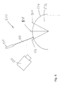
- FIG. 5 shows an improved arrangement 510 for measuring the position of component connections compared to that shown in FIG.
- laser light 542 is emitted by a laser 540 in the direction of the surface 534 of a contact ball 532.
- a camera 550 With a camera 550, light scattered by the surface 534 of the sphere is picked up.
- FIG. 5 shows a boundary of the specular reflection 572 and a limit of shadowing 570, which are such that the most relevant contact area for the ball 532 can be picked up by the camera 550 without disturbing reflections and with sufficient stray light.
- the surface normal 538 of the component connection 532 shown in FIG. 5 is also a rotational symmetry axis of the spherical component connection 532.
- a 3D sensor can be constructed with which the coplanarity of BGAs and Leaded components (in placement machines) can be determined.
Landscapes
- Engineering & Computer Science (AREA)
- Operations Research (AREA)
- Manufacturing & Machinery (AREA)
- Microelectronics & Electronic Packaging (AREA)
- Length Measuring Devices By Optical Means (AREA)
Applications Claiming Priority (1)
| Application Number | Priority Date | Filing Date | Title |
|---|---|---|---|
| DE102006001853 | 2006-01-13 |
Publications (2)
| Publication Number | Publication Date |
|---|---|
| EP1809087A2 true EP1809087A2 (fr) | 2007-07-18 |
| EP1809087A3 EP1809087A3 (fr) | 2013-07-24 |
Family
ID=38093527
Family Applications (1)
| Application Number | Title | Priority Date | Filing Date |
|---|---|---|---|
| EP07100456.8A Withdrawn EP1809087A3 (fr) | 2006-01-13 | 2007-01-12 | Procédé et dispositif destinés à la mesure de coplanarité de connexions de composants |
Country Status (1)
| Country | Link |
|---|---|
| EP (1) | EP1809087A3 (fr) |
Cited By (1)
| Publication number | Priority date | Publication date | Assignee | Title |
|---|---|---|---|---|
| WO2010024681A1 (fr) * | 2008-09-01 | 2010-03-04 | Nederlandse Organisatie Voor Toegepast-Natuurwetenschappelijk Onderzoek Tno | Machine bras-transfert |
Citations (5)
| Publication number | Priority date | Publication date | Assignee | Title |
|---|---|---|---|---|
| EP0472041A2 (fr) | 1990-08-24 | 1992-02-26 | Hitachi, Ltd. | Procédé et dispositif pour détecter des déformations de conducteurs d'un dispositif semi-conducteur |
| US5298977A (en) | 1991-10-16 | 1994-03-29 | Matsushita Electric Industrial Co., Ltd. | Visual inspection method for part mounted on printed circuit board |
| US5598345A (en) | 1990-11-29 | 1997-01-28 | Matsushita Electric Industrial Co., Ltd. | Method and apparatus for inspecting solder portions |
| WO1999008499A1 (fr) | 1997-08-07 | 1999-02-18 | Siemens Aktiengesellschaft | Procede et dispositif pour identifier la position et/ou controler la coplanarite et/ou controler la separation de connexions de composants |
| EP1089607A2 (fr) | 1998-02-27 | 2001-04-04 | Matsushita Electric Industrial Co., Ltd. | Procédé et appareil de reconnaissance des composants |
-
2007
- 2007-01-12 EP EP07100456.8A patent/EP1809087A3/fr not_active Withdrawn
Patent Citations (5)
| Publication number | Priority date | Publication date | Assignee | Title |
|---|---|---|---|---|
| EP0472041A2 (fr) | 1990-08-24 | 1992-02-26 | Hitachi, Ltd. | Procédé et dispositif pour détecter des déformations de conducteurs d'un dispositif semi-conducteur |
| US5598345A (en) | 1990-11-29 | 1997-01-28 | Matsushita Electric Industrial Co., Ltd. | Method and apparatus for inspecting solder portions |
| US5298977A (en) | 1991-10-16 | 1994-03-29 | Matsushita Electric Industrial Co., Ltd. | Visual inspection method for part mounted on printed circuit board |
| WO1999008499A1 (fr) | 1997-08-07 | 1999-02-18 | Siemens Aktiengesellschaft | Procede et dispositif pour identifier la position et/ou controler la coplanarite et/ou controler la separation de connexions de composants |
| EP1089607A2 (fr) | 1998-02-27 | 2001-04-04 | Matsushita Electric Industrial Co., Ltd. | Procédé et appareil de reconnaissance des composants |
Cited By (1)
| Publication number | Priority date | Publication date | Assignee | Title |
|---|---|---|---|---|
| WO2010024681A1 (fr) * | 2008-09-01 | 2010-03-04 | Nederlandse Organisatie Voor Toegepast-Natuurwetenschappelijk Onderzoek Tno | Machine bras-transfert |
Also Published As
| Publication number | Publication date |
|---|---|
| EP1809087A3 (fr) | 2013-07-24 |
Similar Documents
| Publication | Publication Date | Title |
|---|---|---|
| DE69632274T2 (de) | Chromatischer optischer Sensor zum Entfernungsmessen | |
| EP2053913A2 (fr) | Evaluation de la structure de surface d'éléments de construction en utilisant des angles de présentation différents | |
| DE69926659T2 (de) | Verfahren und vorrichtung für die optische Inspektion von Objekten auf einem Substrat | |
| DE19946738B4 (de) | Vorrichtung und Verfahren zum Prüfen von elektrischen Verbindungen an einer Schaltungsplatine | |
| DE102009046262B4 (de) | Optische Messvorrichtung | |
| DE102012102651B3 (de) | Prüfvorrichtung und Prüfverfahren für ein Verkehrsüberwachungsgerät mit einem Laserscanner | |
| DE60015966T2 (de) | Messung der lagen oder koplanarität von kontaktelementen eines elektronischen bauteils mit flacher beleuchtung und zwei kameras | |
| DE102009017695B3 (de) | Verfahren zur Inspektion von Lötstellen an elektrischen und elektronischen Bauteilen | |
| DE3204086A1 (de) | Vorrichtung zur automatischen optischen beschaffenheitspruefung | |
| DE10242373A1 (de) | Konfokaler Abstandssensor | |
| DE3503858A1 (de) | Vorrichtung zur ermittlung von gestaltsfehlern niedriger ordnung | |
| DE19817124A1 (de) | IC-Testgerät | |
| DE102015217332A1 (de) | Positionsmessvorrichtung | |
| DE4408226C2 (de) | Meßeinrichtung zur prozeßgekoppelten Bestimmung der Rauheit technischer Oberflächen durch Auswertung di- oder polychromatischer Specklemuster | |
| DE10014111A1 (de) | Verfahren und Vorrichtung zur Röntgenstrahlprüfung | |
| DE69804984T2 (de) | Beurteilung einer Bump Höhe | |
| EP3575741B1 (fr) | Procédé de mesure sans contact d'un bord de pièce à usiner | |
| DE102011084979B4 (de) | Bildmessgerät | |
| DE10063786A1 (de) | Vorrichtung und Verfahren zum Vermessen eines Gegenstandes | |
| EP1002453B1 (fr) | Procede et dispositif pour identifier la position et/ou controler la coplanarite et/ou controler la separation de connexions de composants | |
| DE102017101102B3 (de) | Verfahren und Koordinatenmessgerät zur Messung von optischen Eigenschaften eines optischen Filters | |
| DE3825228A1 (de) | Verfahren und vorrichtung zum messen des aussendurchmessers eines drahtstifts | |
| DE102018219481A1 (de) | Baugruppe für einen LiDAR-Sensor und LiDAR-Sensor | |
| WO2004055474A1 (fr) | Dispositif de balayage pour la mesure de pieces | |
| WO2004038394A1 (fr) | Procede pour verifier la qualite de billes de connexion de composants electroniques |
Legal Events
| Date | Code | Title | Description |
|---|---|---|---|
| PUAI | Public reference made under article 153(3) epc to a published international application that has entered the european phase |
Free format text: ORIGINAL CODE: 0009012 |
|
| AK | Designated contracting states |
Kind code of ref document: A2 Designated state(s): AT BE BG CH CY CZ DE DK EE ES FI FR GB GR HU IE IS IT LI LT LU LV MC NL PL PT RO SE SI SK TR |
|
| AX | Request for extension of the european patent |
Extension state: AL BA HR MK YU |
|
| RAP1 | Party data changed (applicant data changed or rights of an application transferred) |
Owner name: SIEMENS ELECTRONICS ASSEMBLY SYSTEMS GMBH & CO. KG |
|
| RAP1 | Party data changed (applicant data changed or rights of an application transferred) |
Owner name: ASM ASSEMBLY SYSTEMS GMBH & CO. KG |
|
| PUAL | Search report despatched |
Free format text: ORIGINAL CODE: 0009013 |
|
| AK | Designated contracting states |
Kind code of ref document: A3 Designated state(s): AT BE BG CH CY CZ DE DK EE ES FI FR GB GR HU IE IS IT LI LT LU LV MC NL PL PT RO SE SI SK TR |
|
| AX | Request for extension of the european patent |
Extension state: AL BA HR MK RS |
|
| RIC1 | Information provided on ipc code assigned before grant |
Ipc: H05K 13/04 20060101AFI20130619BHEP Ipc: H05K 13/08 20060101ALI20130619BHEP |
|
| 17P | Request for examination filed |
Effective date: 20140122 |
|
| RBV | Designated contracting states (corrected) |
Designated state(s): AT BE BG CH CY CZ DE DK EE ES FI FR GB GR HU IE IS IT LI LT LU LV MC NL PL PT RO SE SI SK TR |
|
| AKX | Designation fees paid |
Designated state(s): AT |
|
| REG | Reference to a national code |
Ref country code: DE Ref legal event code: R108 |
|
| REG | Reference to a national code |
Ref country code: DE Ref legal event code: R108 Effective date: 20140402 |
|
| RBV | Designated contracting states (corrected) |
Designated state(s): DE |
|
| 17Q | First examination report despatched |
Effective date: 20150917 |
|
| STAA | Information on the status of an ep patent application or granted ep patent |
Free format text: STATUS: THE APPLICATION IS DEEMED TO BE WITHDRAWN |
|
| 18D | Application deemed to be withdrawn |
Effective date: 20160128 |