EP1811433A2 - RFID-Etikett und RFID-System damit - Google Patents
RFID-Etikett und RFID-System damit Download PDFInfo
- Publication number
- EP1811433A2 EP1811433A2 EP07100527A EP07100527A EP1811433A2 EP 1811433 A2 EP1811433 A2 EP 1811433A2 EP 07100527 A EP07100527 A EP 07100527A EP 07100527 A EP07100527 A EP 07100527A EP 1811433 A2 EP1811433 A2 EP 1811433A2
- Authority
- EP
- European Patent Office
- Prior art keywords
- tag
- power
- rfid
- driver
- carrier wave
- Prior art date
- Legal status (The legal status is an assumption and is not a legal conclusion. Google has not performed a legal analysis and makes no representation as to the accuracy of the status listed.)
- Withdrawn
Links
Images



Classifications
-
- E—FIXED CONSTRUCTIONS
- E05—LOCKS; KEYS; WINDOW OR DOOR FITTINGS; SAFES
- E05B—LOCKS; ACCESSORIES THEREFOR; HANDCUFFS
- E05B49/00—Electric permutation locks; Circuits therefor ; Mechanical aspects of electronic locks; Mechanical keys therefor
-
- G—PHYSICS
- G06—COMPUTING OR CALCULATING; COUNTING
- G06K—GRAPHICAL DATA READING; PRESENTATION OF DATA; RECORD CARRIERS; HANDLING RECORD CARRIERS
- G06K19/00—Record carriers for use with machines and with at least a part designed to carry digital markings
- G06K19/06—Record carriers for use with machines and with at least a part designed to carry digital markings characterised by the kind of the digital marking, e.g. shape, nature, code
- G06K19/067—Record carriers with conductive marks, printed circuits or semiconductor circuit elements, e.g. credit or identity cards also with resonating or responding marks without active components
- G06K19/07—Record carriers with conductive marks, printed circuits or semiconductor circuit elements, e.g. credit or identity cards also with resonating or responding marks without active components with integrated circuit chips
- G06K19/0723—Record carriers with conductive marks, printed circuits or semiconductor circuit elements, e.g. credit or identity cards also with resonating or responding marks without active components with integrated circuit chips the record carrier comprising an arrangement for non-contact communication, e.g. wireless communication circuits on transponder cards, non-contact smart cards or RFIDs
-
- H—ELECTRICITY
- H10—SEMICONDUCTOR DEVICES; ELECTRIC SOLID-STATE DEVICES NOT OTHERWISE PROVIDED FOR
- H10D—INORGANIC ELECTRIC SEMICONDUCTOR DEVICES
- H10D1/00—Resistors, capacitors or inductors
- H10D1/60—Capacitors
- H10D1/62—Capacitors having potential barriers
- H10D1/64—Variable-capacitance diodes, e.g. varactors
-
- H—ELECTRICITY
- H10—SEMICONDUCTOR DEVICES; ELECTRIC SOLID-STATE DEVICES NOT OTHERWISE PROVIDED FOR
- H10D—INORGANIC ELECTRIC SEMICONDUCTOR DEVICES
- H10D1/00—Resistors, capacitors or inductors
- H10D1/60—Capacitors
- H10D1/62—Capacitors having potential barriers
- H10D1/66—Conductor-insulator-semiconductor capacitors, e.g. MOS capacitors
-
- H—ELECTRICITY
- H10—SEMICONDUCTOR DEVICES; ELECTRIC SOLID-STATE DEVICES NOT OTHERWISE PROVIDED FOR
- H10D—INORGANIC ELECTRIC SEMICONDUCTOR DEVICES
- H10D84/00—Integrated devices formed in or on semiconductor substrates that comprise only semiconducting layers, e.g. on Si wafers or on GaAs-on-Si wafers
- H10D84/80—Integrated devices formed in or on semiconductor substrates that comprise only semiconducting layers, e.g. on Si wafers or on GaAs-on-Si wafers characterised by the integration of at least one component covered by groups H10D12/00 or H10D30/00, e.g. integration of IGFETs
- H10D84/811—Combinations of field-effect devices and one or more diodes, capacitors or resistors
-
- H—ELECTRICITY
- H10—SEMICONDUCTOR DEVICES; ELECTRIC SOLID-STATE DEVICES NOT OTHERWISE PROVIDED FOR
- H10D—INORGANIC ELECTRIC SEMICONDUCTOR DEVICES
- H10D84/00—Integrated devices formed in or on semiconductor substrates that comprise only semiconducting layers, e.g. on Si wafers or on GaAs-on-Si wafers
- H10D84/80—Integrated devices formed in or on semiconductor substrates that comprise only semiconducting layers, e.g. on Si wafers or on GaAs-on-Si wafers characterised by the integration of at least one component covered by groups H10D12/00 or H10D30/00, e.g. integration of IGFETs
- H10D84/811—Combinations of field-effect devices and one or more diodes, capacitors or resistors
- H10D84/813—Combinations of field-effect devices and capacitor only
-
- G—PHYSICS
- G07—CHECKING-DEVICES
- G07C—TIME OR ATTENDANCE REGISTERS; REGISTERING OR INDICATING THE WORKING OF MACHINES; GENERATING RANDOM NUMBERS; VOTING OR LOTTERY APPARATUS; ARRANGEMENTS, SYSTEMS OR APPARATUS FOR CHECKING NOT PROVIDED FOR ELSEWHERE
- G07C9/00—Individual registration on entry or exit
- G07C9/00174—Electronically operated locks; Circuits therefor; Nonmechanical keys therefor, e.g. passive or active electrical keys or other data carriers without mechanical keys
- G07C2009/00968—Electronically operated locks; Circuits therefor; Nonmechanical keys therefor, e.g. passive or active electrical keys or other data carriers without mechanical keys shape of the data carrier
- G07C2009/00976—Electronically operated locks; Circuits therefor; Nonmechanical keys therefor, e.g. passive or active electrical keys or other data carriers without mechanical keys shape of the data carrier card
-
- G—PHYSICS
- G07—CHECKING-DEVICES
- G07C—TIME OR ATTENDANCE REGISTERS; REGISTERING OR INDICATING THE WORKING OF MACHINES; GENERATING RANDOM NUMBERS; VOTING OR LOTTERY APPARATUS; ARRANGEMENTS, SYSTEMS OR APPARATUS FOR CHECKING NOT PROVIDED FOR ELSEWHERE
- G07C9/00—Individual registration on entry or exit
- G07C9/00174—Electronically operated locks; Circuits therefor; Nonmechanical keys therefor, e.g. passive or active electrical keys or other data carriers without mechanical keys
- G07C9/00563—Electronically operated locks; Circuits therefor; Nonmechanical keys therefor, e.g. passive or active electrical keys or other data carriers without mechanical keys using personal physical data of the operator, e.g. finger prints, retinal images, voicepatterns
Definitions
- the present invention relates to a radio frequency identification (RFID) tag and an RFID system having the same. More particularly, the present invention relates to an RFID tag to stably control impedance on transmitting a carrier wave and an RFID system having the same.
- RFID radio frequency identification
- RFID is an automatic recognition technology using wireless frequencies and is a representative new technology of a contactless integrated circuit (IC) card to replace a barcode and a magnetic card.
- IC contactless integrated circuit
- the RFID system includes an RFID reader, a host computer and a transponder, that is, an RFID tag.
- the RFID reader transmits radio waves to the RFID tag, and the RFID tag receives the radio waves and transmits corresponding data to the RFID reader.
- the RFID tag includes an antenna transmitting and receiving radio waves to/from the RFID reader and a driving chip storing data such as identification information to identify each RFID tag. If the RFID tag receives radio waves from the RFID reader, the RFID tag transmits the corresponding data including the identification information to the RFID reader.
- the RFID tag separates into active and passive tags according to the operation method.
- the active RFID tag has a power source to drive itself.
- the passive RFID tag does not have a power source to drive itself, but receives radio waves and a power to drive itself from the RFID reader.
- the passive RFID tag After receiving an input power, the passive RFID tag generates a carrier wave and transmits a carrier power to the RFID reader.
- the RFID tag loads predetermined data including the identification information into the carrier wave, modulates the data into electric signals and transmits the power to the RFID reader.
- the RFID tag adjusts a resistance corresponding to the driving chip by turning on/off a transistor embedded in the driving chip on transmitting the carrier wave, so that impedance of the driving chip is adjusted. Impedance adjustment of the RFID tag is essential to minimize reflection signals between the RFID reader and the RFID tag. That is, if impedance matching between the RFID reader and the RFID tag is not accurately performed, a reflection coefficient between the RFID reader and the RFID tag become high and the reflection signals increase so that power loss of the RFID reader increases.
- the RFID tag adjusts resistance of the driving chip according to the size of the carrier wave for impedance matching using a modulation transistor.
- FIG. 1 is a graph illustrating an output voltage of the RFID tag corresponding to signal transmission and reception in a related art RFID system.
- the RFID reader transmits an input power (IP) and the RFID tag receives the IP.
- the RFID tag transmits a reflection power (RP) to transmit a carrier wave corresponding to the IP to the RFID reader.
- the RP contains a carrier wave modulated to include a signal wave indicating the identification information of the RFID tag.
- the amplitude of the carrier wave varies corresponding to the amplitude of the signal wave, that is, a digital data value of the signal wave in the modulation process. That is, the driving chip of the RFID tag changes the amplitude of the carrier wave by adjusting the voltage. Accordingly, the impedance of the driving chip can vary corresponding to the amplitude variation of the data signal.
- the RFID tag modifies a resistance of the driving chip using the modulation transistor. That is, the modulation transistor is turned on/off corresponding to the amplitude variation of the carrier wave to adjust the current of the driving chip. Accordingly, the RFID tag can adjust the resistance of the driving chip so that the impedance of the driving chip can be adjusted.
- the modulation transistor is turned on so that current consumption increases, the intensity of voltage transmitted from the driving chip can be lower than the reference voltage Vdd (A, B).
- Vdd the reference voltage
- the voltage output from the RFID tag that is, the voltage transmitted from the driving chip has to be higher than the reference voltage Vdd. If the modulation transistor is turned off again, the current consumption is suddenly reduced. Accordingly, the voltage output from the driving chip is higher than the reference voltage Vdd.
- circuits embedded in the RFID tag can unstably drive. Accordingly, the power supply of the RFID tag is unstable, and modulation and demodulation are unstable, so that signal transmission/reception between the RFID reader and the RFID tag cannot be normally performed.
- Exemplary embodiments of the present invention overcome the above disadvantages and other disadvantages not described above. Also, the present invention is not required to overcome the disadvantages described above, and an exemplary embodiment of the present invention may not overcome any of the problems described above.
- radio frequency identification (RFID) tag comprising:
- the present invention thus provides an RFID tag which can improve the reliability of products by stably adjusting the voltage on transmission of a carrier wave.
- the tag driver preferably comprises a memory storing data, a controller detecting the data from the memory corresponding to the input power, modulating the carrier wave, and generating the reflection power with the carrier wave modulated corresponding to the input power; and an accumulation mode capacitor adjusting an impedance of the tag driver by adaptively adjusting the capacitance according to the intensity of a voltage of the reflection power, and receiving the reflection power from the controller and providing the reflection power to the tag antenna.
- the capacitance value increases, and if the voltage of the reflection power is higher than the threshold voltage, the capacitance value decreases.
- the accumulation mode capacitor may comprise at least one varactor connected to an input pad and ground pad of the RFID antenna.
- the varactor comprises a gate part receiving the voltage of the reflection power, a source part, and a drain part connected to the source part, and the gate part is electrically connected to a connecting line which connects the source part and the drain part.
- the capacitance value is changed if the reflection power is higher than a minimum power for backscattering, which modulates the carrier wave and loads the signal wave including the data into the carrier wave.
- the effective power may be an effective isotropic radiation power of the tag antenna, and the minimum power for backscattering may be approximately -70dBm.
- the tag driver keeps a predetermined impedance regardless of amplitude variation of the carrier wave modulated through backscattering.
- the impedance of the tag antenna may be a complex conjugate of the impedance of the tag driver.
- the present invention also provides an RFID system including the RFID.
- radio frequency identification (RFID) system comprising:
- the RFID tag can adjust the impedance of the tag driver by adjusting the capacitance value, it can prevent the voltage transmitted from the tag driver from being lower than the reference voltage, and modulation and demodulation can be stably performed. As a result, the reliability of products can be enhanced.
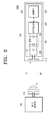
- FIG. 2 is a schematic diagram illustrating an RFID system according to an exemplary embodiment of the present invention.
- the RFID system 1000 includes an RFID reader 100 and an RFID tag 200.
- the RFID reader 100 includes an antenna 110 radiating a radio wave and transmits/receives data to/from the RFID tag 200 using radio frequency.
- the RFID tag 200 stores predetermined data including an identifier (ID) given for each RFID tag to identify each RFID tag. If the RFID tag 200 is located in the read range of the RFID reader 100, that is, in the magnetic field or electrical field, the RFID tag 200 receives waves radiated from the RFID reader 100. The wave output from the RFID reader 100 includes an input power IP to drive the RFID tag 200.
- ID an identifier
- the RFID tag 200 If the RFID tag 200 receives the input power IP from the RFID reader 100, the RFID tag 200 transmits the data including the ID to the RFID reader 100. That is, the RFID tag 200 transmits a reflection power RP including the data to the RFID reader 100, corresponding to the input power IP.
- the RFID tag 200 includes a tag antenna 210 transmitting/receiving waves to/from the RFID reader 100 and a tag driver 220 generating the reflection power RP using the input power IP.
- the tag antenna 210 receives an input power IP from the RFID reader 100 to transmit to the tag driver 220, and receives a reflection power RP from the tag driver 220 to radiate to the RFID reader 100.
- the RFID reader 100 authenticates the RFID tag 200 using the data included in the reflection power RP.
- the tag driver 220 is connected to an input pad and ground pad of the tag antenna 210.
- the tag driver 220 can consist of at least one element.
- the tag driver 220 includes a rectifier 221, a smoother 223, a controller 225, a memory 227 and an accumulation mode capacitor 229.
- the rectifier 221 converts the input power IP from alternating current to direct current.
- the smoother 223 is connected to the rectifier 221 in parallel and outputs the input voltage by converting an alternating current component of the power output from the rectifier 221 into direct current.
- the input voltage is used to drive internal elements including the controller 225 and the memory 227.
- the controller 225 receives the input voltage from the smoother 223 and generates a reflection power RP using data stored in the memory 227 and the input power IP.
- the memory 227 stores the ID to identify the RFID tag 200 and other data.
- the controller 225 detects the ID from the memory 227 corresponding to the input power IP and generates a signal wave including the detected ID.
- the signal wave can carry the ID of the RFID tag 200 and other data.
- the controller 225 modulates and outputs the carrier wave according to the signal wave, corresponding to the input power IP.
- the controller 225 performs modulation by adjusting a voltage in order for the amplitude of the carrier wave to vary corresponding to the amplitude of the signal wave and this kind of modulation method is called amplitude modulation.
- the controller 225 modifies the amplitude of the carrier wave by adjusting an output voltage Vc of the tag driver 220, that is, the intensity of the voltage of the carrier power RP, and the amplitude of the signal wave varies according to a digital signal corresponding to the signal wave.
- the modulated carrier wave is included in the reflection power RP and transmitted to the RFID reader 100 through the tag antenna 210.
- the RFID reader 100 demodulates the carrier wave and reads the ID of the RFID tag 200. Accordingly, the RFID reader 100 authenticates the RFID tag 200.
- the process in which the RFID tag 200 modulates the carrier wave and transmits the carrier wave to the RFID reader 100 is called backscattering.
- the accumulation mode capacitor 229 is connected to the tag antenna 210 in parallel.
- the accumulation mode capacitor 229 adjusts the capacitance value corresponding to the value of the output voltage Vc so that the impedance of the tag driver 220 is adjusted.
- the impedance of the tag driver 220 adjusted by the capacitance value of the tag driver 220, the intensity of the current of the tag driver 220 and the intensity of the output voltage Vc.
- the tag driver 220 adjusts the amplitude of the carrier wave by adjusting the voltage in the process of modulating the carrier wave. Accordingly, the intensity of the output voltage Vc is adjusted by the size of the amplitude of the modulated carrier wave so that the impedance of the tag driver 220 varies according to the size of the amplitude of the carrier wave.
- the impedance of the tag driver 220 has to keep a regular value regardless of the size of the amplitude of the carrier wave for impedance matching with the tag antenna 210.
- the tag driver 220 must maintain the impedance of a regular value for impedance matching with the tag antenna 210, but the impedance Zc of the tag driver 220 can be changed according to the amplitude of the modulated carrier wave.
- the accumulation mode capacitor 229 adjusts its capacitance value corresponding to the output voltage so that the tag driver 220 can maintain the regular impedance regardless of the intensity of the output voltage Vc. That is, in the accumulation mode capacitor 229, if the output voltage Vc increases, the capacitance value decreases, and if the output voltage Vc decreases, the capacitance value increases.
- the capacitance value of the accumulation mode capacitor 229 is inversely proportional to the intensity of the output voltage Vc and the accumulation mode capacitor 229 compensates impedance variation occurred due to the intensity difference of the output voltage Vc. Therefore, the tag driver 220 can maintain the impedance regular regardless of the size of the amplitude of the modulated carrier wave.
- the RFID tag 200 adjusts the impedance by adjusting the capacitance value according to the size of the amplitude of the carrier wave, so that the intensity of the voltage and current transmitted from the tag driver 220 does not need to be adjusted for impedance adjustment. Accordingly, the RFID tag 200 can prevent the output voltage Vc transmitted from the tag driver 220 from being lower than the reference voltage, and modulation and demodulation can be stably performed so that the reliability of products can be enhanced.
- the RFID tag 200 does not need a transistor to adjust the impedance, power consumption by turning on/off the transistor can be prevented and the low-power RFID tag 200 can be implemented.
- the RFID tag 200 can enhance impedance matching between the tag antenna 210 and the tag driver 220, the reflection coefficient between the RFID reader 100 and the RFID tag 200 can be reduced. Accordingly, the RFID system 1000 can enhance power use efficiency and extend the read range of the RFID reader 100.
- FIG. 3 is a perspective view illustrating a varactor applied to the accumulation mode capacitor of FIG. 2, and FIG. 4 is a circuit diagram illustrating the varactor of FIG. 3.
- the accumulation mode capacitor 229 includes at least one metal oxide semiconductor (MOS) varactor 229a.
- the varactor 229a is a variable capacitance diode whose capacitor's value varies according to the input voltage.
- the varactor 229a includes a gate part G formed on a base substrate B, a source part S and a drain part D.
- the area adjacent to where the gate part G is formed on the base substrate B is doped with n+.
- the output voltage Vc is transmitted to the gate part G.
- the source part S and the drain part D are electrically connected to each other, and a line which connects the source part S and the drain part D is electrically connected to the gate part G.
- the capacitance value increases. However, if the output voltage Vc to be input to the gate part G in the varactor 229a is transmitted higher than a threshold voltage, the capacitance value decreases.
- FIG. 5 is a graph illustrating the relation between capacitance and source part-gate part voltage in the accumulation mode capacitor of FIG. 2.
- the capacitance value gradually decreases.
- the capacitance value sharply increases.
- the reference power is a minimum power by which the RFID reader 100 can read the RFID tag 200 and is also a minimum power P bs required for backscattering.
- I 1 and I 2 are the current of the tag driver 220, and R rad is the radiation resistance of the tag antenna 210.
- the current of the tag driver 220 is referred to as the first current I 1
- the current of the tag driver 220 is referred to as the second current I 2 .
- V a is the voltage transmitted to the tag antenna 210 by the input power IP
- Z a is the impedance of the tag antenna 210
- Z 1 and Z 2 are the impedances of the tag driver 220.
- the impedance of the tag driver 220 is referred to as the first impedance Z 1
- the impedance of the tag driver 220 is referred to as the second impedance Z 2 .
- I 1 and I 2 can be calculated using the voltage V a transmitted to the tag antenna 210, the real number impedance R a of the tag antenna 210, and the first and second reflection coefficients ⁇ 1 and ⁇ 2 .
- the reflection coefficient is referred to as the first reflection coefficient ⁇ 1
- the reflection coefficient is referred to as the second reflection coefficient ⁇ 2 .
- the impedances Z 1 and Z 2 of the tag driver 220 may be complex conjugate values of the impedance Z a of the tag antenna 210 for impedance matching with the tag antenna 210. As described above, the impedances Z 1 and Z 2 of the tag driver 220 have to be equal to complex conjugate values of the impedance Z a of the tag antenna 210 regardless of the amplitude of the signal wave for impedance matching with the tag antenna 210. To this end, the accumulation mode capacitor 229 adjusts the capacitance value according to the amplitude of the signal wave to make the first and second impedances Z 1 and Z 2 equal.
- the average power to drive the tag driver 220 is lower than approximately 50% of an effective power P a .
- the effective power P a is a power provided from the tag antenna 210 to the tag driver 220 and indicates effective isotropic radiated power (EIRP) of the tag antenna 210.
- EIRP effective isotropic radiated power
- the effective power Pa is approximately 4W.
- the minimum power Pbs of the tag driver 220 is approximately 10- 10 W, that is, approximately -70dBm. That is, when the reflection power RP transmitted from the tag driver 220 is over approximately -70dBm, the RFID reader 100 can recognize the RFID tag 200. Therefore, the accumulation mode capacitor 229 changes the capacitance value in the state that the reflection power RP is over approximately -70dBm.
- the RFID tag includes the accumulation mode capacitor which adjusts the capacitance value according to the amplitude of the modulated carrier wave. Accordingly, the RFID tag adjusts the capacitance value to adjust the amplitude of the carrier wave without adjusting the voltage and current transmitted from the tag driver. Therefore, as the RFID tag can adjust the impedance by adjusting the capacitance value, it can prevent the voltage transmitted from the tag driver from being lower than the reference voltage, and modulation and demodulation can be stably performed. As a result, the reliability of products can be enhanced.
- the RFID tag does not need a transistor to adjust the impedance, power consumption by turning on/off the transistor can be prevented and a low-power RFID tag can be implemented.
- the tag driver can adjust the capacitance value for precise impedance matching with the tag antenna so that reflection signals between the RFID tag and the RFID reader can be reduced. Consequently, the RFID system can enhance power use efficiency and the read range of the RFID reader can be extended.
Landscapes
- Engineering & Computer Science (AREA)
- Computer Networks & Wireless Communication (AREA)
- Computer Hardware Design (AREA)
- Microelectronics & Electronic Packaging (AREA)
- Physics & Mathematics (AREA)
- General Physics & Mathematics (AREA)
- Theoretical Computer Science (AREA)
- Near-Field Transmission Systems (AREA)
Applications Claiming Priority (1)
| Application Number | Priority Date | Filing Date | Title |
|---|---|---|---|
| KR1020060006463A KR100732681B1 (ko) | 2006-01-20 | 2006-01-20 | Rfid 태그 및 이를 갖는 rfid 시스템 |
Publications (2)
| Publication Number | Publication Date |
|---|---|
| EP1811433A2 true EP1811433A2 (de) | 2007-07-25 |
| EP1811433A3 EP1811433A3 (de) | 2009-02-11 |
Family
ID=37989852
Family Applications (1)
| Application Number | Title | Priority Date | Filing Date |
|---|---|---|---|
| EP07100527A Withdrawn EP1811433A3 (de) | 2006-01-20 | 2007-01-15 | RFID-Etikett und RFID-System damit |
Country Status (4)
| Country | Link |
|---|---|
| US (1) | US7595729B2 (de) |
| EP (1) | EP1811433A3 (de) |
| JP (1) | JP4732320B2 (de) |
| KR (1) | KR100732681B1 (de) |
Cited By (1)
| Publication number | Priority date | Publication date | Assignee | Title |
|---|---|---|---|---|
| CN105005751A (zh) * | 2015-08-12 | 2015-10-28 | 苏州芯动科技有限公司 | 一种rfid标签芯片信号反射方法 |
Families Citing this family (24)
| Publication number | Priority date | Publication date | Assignee | Title |
|---|---|---|---|---|
| US7439860B2 (en) * | 2006-03-22 | 2008-10-21 | Assa Abloy Ab | Auto-tuned RFID reader antenna |
| US8226003B2 (en) | 2006-04-27 | 2012-07-24 | Sirit Inc. | Adjusting parameters associated with leakage signals |
| US8248212B2 (en) | 2007-05-24 | 2012-08-21 | Sirit Inc. | Pipelining processes in a RF reader |
| US20090135005A1 (en) * | 2007-11-06 | 2009-05-28 | David Novak | Tracking and security system |
| WO2009089507A1 (en) * | 2008-01-11 | 2009-07-16 | Mu-Gahat Holdings Inc. | Enhancing the efficiency of energy transfer to/from passive id circuits using ferrite cores |
| WO2009108702A1 (en) * | 2008-02-25 | 2009-09-03 | Mu-Gahat Holdings, Inc | Extending the read range of passive rfid tags |
| US8339266B2 (en) * | 2008-03-11 | 2012-12-25 | Intermec Ip Corp. | System and method for determining RFID tag placement |
| US8427316B2 (en) | 2008-03-20 | 2013-04-23 | 3M Innovative Properties Company | Detecting tampered with radio frequency identification tags |
| US8395507B2 (en) | 2008-04-21 | 2013-03-12 | Magnet Consulting, Inc. | H-field shaping using a shorting loop |
| US8446256B2 (en) | 2008-05-19 | 2013-05-21 | Sirit Technologies Inc. | Multiplexing radio frequency signals |
| US8169312B2 (en) | 2009-01-09 | 2012-05-01 | Sirit Inc. | Determining speeds of radio frequency tags |
| JP2012528413A (ja) * | 2009-05-28 | 2012-11-12 | コヴィオ インコーポレイテッド | 無線デバイスからコードを有効化する方法およびシステム |
| US8416079B2 (en) | 2009-06-02 | 2013-04-09 | 3M Innovative Properties Company | Switching radio frequency identification (RFID) tags |
| KR101139491B1 (ko) | 2010-09-08 | 2012-05-02 | 에스케이하이닉스 주식회사 | Rfid 장치 |
| US10062025B2 (en) | 2012-03-09 | 2018-08-28 | Neology, Inc. | Switchable RFID tag |
| US9430729B2 (en) * | 2012-05-31 | 2016-08-30 | Nxp B.V. | Broadband progressive tag |
| JP2014006591A (ja) * | 2012-06-21 | 2014-01-16 | Nakayo Telecommun Inc | 負荷変動型無線タグリーダおよび無線タグ |
| US9542638B2 (en) | 2014-02-18 | 2017-01-10 | Apple Inc. | RFID tag and micro chip integration design |
| US9618366B2 (en) * | 2014-11-25 | 2017-04-11 | Mitutoyo Corporation | Absolute encoder scale configuration with unique coded impedance modulations |
| US10572789B1 (en) * | 2015-06-26 | 2020-02-25 | Impinj, Inc. | Impedance-change mitigation in RFID tags |
| US9886658B1 (en) * | 2015-06-26 | 2018-02-06 | Impinj, Inc | Impedance-change mitigation in RFID tags |
| KR20170017164A (ko) | 2015-08-05 | 2017-02-15 | 한국전자통신연구원 | 복수의 안테나를 구비한 무선 주파수 식별 태그 |
| CN106934446B (zh) * | 2017-04-21 | 2023-09-15 | 中国科学院上海高等研究院 | 适用于超高频rfid标签的调制器及其控制方法 |
| CN109447223B (zh) * | 2018-10-31 | 2021-09-14 | 华大恒芯科技有限公司 | 一种增强超高频rfid标签反射功率的方法 |
Family Cites Families (18)
| Publication number | Priority date | Publication date | Assignee | Title |
|---|---|---|---|---|
| US5548821A (en) * | 1992-06-09 | 1996-08-20 | Coveley; Michael | Adaptive system for self-tuning and selecting a carrier frequency in a radio frequency communication system |
| US5598169A (en) * | 1995-03-24 | 1997-01-28 | Lucent Technologies Inc. | Detector and modulator circuits for passive microwave links |
| US5606323A (en) * | 1995-08-31 | 1997-02-25 | International Business Machines Corporation | Diode modulator for radio frequency transponder |
| SG54559A1 (en) * | 1996-09-13 | 1998-11-16 | Hitachi Ltd | Power transmission system ic card and information communication system using ic card |
| FR2757952B1 (fr) * | 1996-12-27 | 1999-03-19 | Gemplus Card Int | Transpondeur radioelectrique muni d'une antenne et d'un circuit de desaccord en frequence |
| JP3621560B2 (ja) * | 1997-07-24 | 2005-02-16 | 三菱電機株式会社 | 電磁誘導型データキャリアシステム |
| FR2776781B1 (fr) * | 1998-03-31 | 2000-05-05 | Gemplus Card Int | Dispositif de controle de l'impedance ramenee sur l'antenne d'une etiquette electromagnetique |
| FR2801745B1 (fr) * | 1999-11-30 | 2007-05-25 | St Microelectronics Sa | Transpondeur electromagnetique a desaccord en frequence |
| US7235862B2 (en) * | 2001-07-10 | 2007-06-26 | National Semiconductor Corporation | Gate-enhanced junction varactor |
| US6870461B2 (en) * | 2001-12-01 | 2005-03-22 | Atmel Germany Gmbh | Integrated receiving/backscattering arrangement for contactless data transmission |
| JP4238005B2 (ja) * | 2002-10-15 | 2009-03-11 | 富士通マイクロエレクトロニクス株式会社 | 電圧可変容量素子およびその製造方法、半導体集積回路装置 |
| DE10301451A1 (de) * | 2003-01-10 | 2004-07-22 | Atmel Germany Gmbh | Verfahren sowie Sende- und Empfangseinrichtung zur drahtlosen Datenübertragung und Modulationseinrichtung |
| DE10357665A1 (de) * | 2003-01-10 | 2004-07-22 | Atmel Germany Gmbh | Schaltungsanordnung zur Bereitstellung elektrischer Leistung aus einem elektromagnetischen Feld |
| DE10325399A1 (de) * | 2003-05-28 | 2004-12-30 | Atmel Germany Gmbh | Schaltungsanordnung zur Phasenmodulation für rückstreubasierte Transporder |
| US7747271B2 (en) * | 2005-03-02 | 2010-06-29 | Qualcomm Incorporated | Radiated power control for a multi-antenna transmission |
| US7586384B2 (en) * | 2005-08-15 | 2009-09-08 | Nokia Corporation | Integrated load impedance sensing for tunable matching networks |
| US20070098118A1 (en) * | 2005-11-01 | 2007-05-03 | Khurram Muhammad | Method for automatic gain control (AGC) by combining if frequency adjustment with receive path gain adjustment |
| KR100659272B1 (ko) | 2005-12-15 | 2006-12-20 | 삼성전자주식회사 | 과전압 제어가 가능한 무선인증용 태그 및 그의 과전압제어 방법 |
-
2006
- 2006-01-20 KR KR1020060006463A patent/KR100732681B1/ko not_active Expired - Fee Related
- 2006-10-20 US US11/583,936 patent/US7595729B2/en not_active Expired - Fee Related
- 2006-12-15 JP JP2006339097A patent/JP4732320B2/ja not_active Expired - Fee Related
-
2007
- 2007-01-15 EP EP07100527A patent/EP1811433A3/de not_active Withdrawn
Cited By (2)
| Publication number | Priority date | Publication date | Assignee | Title |
|---|---|---|---|---|
| CN105005751A (zh) * | 2015-08-12 | 2015-10-28 | 苏州芯动科技有限公司 | 一种rfid标签芯片信号反射方法 |
| CN105005751B (zh) * | 2015-08-12 | 2017-09-22 | 苏州芯动科技有限公司 | 一种rfid标签芯片信号反射方法 |
Also Published As
| Publication number | Publication date |
|---|---|
| KR100732681B1 (ko) | 2007-06-27 |
| US7595729B2 (en) | 2009-09-29 |
| JP4732320B2 (ja) | 2011-07-27 |
| JP2007193780A (ja) | 2007-08-02 |
| EP1811433A3 (de) | 2009-02-11 |
| US20070171065A1 (en) | 2007-07-26 |
Similar Documents
| Publication | Publication Date | Title |
|---|---|---|
| EP1811433A2 (de) | RFID-Etikett und RFID-System damit | |
| EP2341603A1 (de) | Ladepumpenstufe eines Transponders zur Identifizierung der Funkfrequenz | |
| US8319611B2 (en) | Radio frequency indentification tag | |
| US7173519B2 (en) | Circuit arrangement with simplified input circuit for phase modulation in a backscattering transponder | |
| US6940467B2 (en) | Circuit arrangement and method for deriving electrical power from an electromagnetic field | |
| US8810375B2 (en) | Semiconductor device and IC label, IC tag, and IC card having the same | |
| US8174390B2 (en) | Radio frequency identification tag and antenna for radio frequency identification tag | |
| US8243863B2 (en) | Semiconductor device | |
| JP3475996B2 (ja) | 非接触icカードシステム、icカード用のカードリーダ及びicカード | |
| AU2003220174A2 (en) | Integrated circuit with enhanced coupling | |
| US6626363B2 (en) | Antenna device and card-shaped storage medium | |
| AU2009202318A1 (en) | Rectifier utilizing a grounded antenna | |
| US20070164122A1 (en) | Contactless card and contactless card system | |
| JP5290170B2 (ja) | 識別対象物に取り付けられる無線識別デバイス(rfid) | |
| US7629929B2 (en) | Antenna using proximity-coupled feed method, RFID tag having the same, and antenna impedance matching method thereof | |
| JP4690455B2 (ja) | 改良された電圧制限回路を有するトランスポンダ | |
| CN101479955A (zh) | 以具有多个天线为特征的非接触式射频设备以及相关的天线选择电路 | |
| KR100932558B1 (ko) | 전파 식별 태그 및 전파 식별 태그 안테나 | |
| WO2007089106A1 (en) | Antenna using proximity-coupling between radiation patch and short-ended feed line, rfid tag employing the same, and antenna impedance matching method thereof | |
| KR100453721B1 (ko) | 수동 트랜스폰더 장치 | |
| KR20120116028A (ko) | Rfid 태그용 마이크로스트립 안테나 | |
| KR100792256B1 (ko) | Rfid 트랜스폰더를 위한 렉테나 | |
| KR20150082898A (ko) | 마이크로스트립 안테나 | |
| HK1136099A (en) | Device with no radiofrequency contact comprising several antennas and associated antenna selection circuit | |
| JP2012138007A (ja) | 非接触式携帯可能電子装置および非接触式icカード |
Legal Events
| Date | Code | Title | Description |
|---|---|---|---|
| PUAI | Public reference made under article 153(3) epc to a published international application that has entered the european phase |
Free format text: ORIGINAL CODE: 0009012 |
|
| AK | Designated contracting states |
Kind code of ref document: A2 Designated state(s): AT BE BG CH CY CZ DE DK EE ES FI FR GB GR HU IE IS IT LI LT LU LV MC NL PL PT RO SE SI SK TR |
|
| AX | Request for extension of the european patent |
Extension state: AL BA HR MK YU |
|
| RIN1 | Information on inventor provided before grant (corrected) |
Inventor name: LEE, DONG-HYUN Inventor name: LEE, SEONG-HEARN Inventor name: KU, JA-NAM |
|
| PUAL | Search report despatched |
Free format text: ORIGINAL CODE: 0009013 |
|
| AK | Designated contracting states |
Kind code of ref document: A3 Designated state(s): AT BE BG CH CY CZ DE DK EE ES FI FR GB GR HU IE IS IT LI LT LU LV MC NL PL PT RO SE SI SK TR |
|
| AX | Request for extension of the european patent |
Extension state: AL BA HR MK RS |
|
| RIC1 | Information provided on ipc code assigned before grant |
Ipc: H04B 1/18 20060101ALI20090108BHEP Ipc: H03H 7/40 20060101ALI20090108BHEP Ipc: H01P 5/04 20060101ALI20090108BHEP Ipc: H01L 29/93 20060101ALI20090108BHEP Ipc: H01L 27/08 20060101ALI20090108BHEP Ipc: G06K 19/07 20060101AFI20070510BHEP |
|
| AKX | Designation fees paid | ||
| REG | Reference to a national code |
Ref country code: DE Ref legal event code: 8566 |
|
| STAA | Information on the status of an ep patent application or granted ep patent |
Free format text: STATUS: THE APPLICATION IS DEEMED TO BE WITHDRAWN |
|
| 18D | Application deemed to be withdrawn |
Effective date: 20090812 |