EP1811596A1 - Hochfrequenz-Wellenleiter mit elektrischem Leiter aus einer mit einer leitfähigen Schicht beschichteten Plastikfolie - Google Patents
Hochfrequenz-Wellenleiter mit elektrischem Leiter aus einer mit einer leitfähigen Schicht beschichteten Plastikfolie Download PDFInfo
- Publication number
- EP1811596A1 EP1811596A1 EP06290148A EP06290148A EP1811596A1 EP 1811596 A1 EP1811596 A1 EP 1811596A1 EP 06290148 A EP06290148 A EP 06290148A EP 06290148 A EP06290148 A EP 06290148A EP 1811596 A1 EP1811596 A1 EP 1811596A1
- Authority
- EP
- European Patent Office
- Prior art keywords
- layer
- electric conductive
- waveguide
- conductive material
- sheet
- Prior art date
- Legal status (The legal status is an assumption and is not a legal conclusion. Google has not performed a legal analysis and makes no representation as to the accuracy of the status listed.)
- Granted
Links
- 239000004020 conductor Substances 0.000 title claims abstract description 119
- 239000004033 plastic Substances 0.000 title claims abstract description 42
- 229920003023 plastic Polymers 0.000 title claims abstract description 42
- 239000011888 foil Substances 0.000 title claims description 44
- 238000000034 method Methods 0.000 claims abstract description 27
- 238000004519 manufacturing process Methods 0.000 claims abstract description 12
- 239000000463 material Substances 0.000 claims description 12
- 238000002788 crimping Methods 0.000 claims description 8
- 238000009957 hemming Methods 0.000 claims description 8
- 239000011152 fibreglass Substances 0.000 claims description 6
- 238000010030 laminating Methods 0.000 claims description 6
- 238000005530 etching Methods 0.000 claims description 5
- 239000004744 fabric Substances 0.000 claims description 5
- 230000005855 radiation Effects 0.000 claims description 4
- 239000004642 Polyimide Substances 0.000 claims description 3
- 239000000654 additive Substances 0.000 claims description 3
- 229920001721 polyimide Polymers 0.000 claims description 3
- 229920000098 polyolefin Polymers 0.000 claims description 3
- 230000002787 reinforcement Effects 0.000 claims description 3
- 238000005476 soldering Methods 0.000 claims description 3
- RYGMFSIKBFXOCR-UHFFFAOYSA-N Copper Chemical compound [Cu] RYGMFSIKBFXOCR-UHFFFAOYSA-N 0.000 description 10
- 229910052802 copper Inorganic materials 0.000 description 10
- 239000010949 copper Substances 0.000 description 10
- 238000005452 bending Methods 0.000 description 7
- 239000007787 solid Substances 0.000 description 7
- BQCADISMDOOEFD-UHFFFAOYSA-N Silver Chemical compound [Ag] BQCADISMDOOEFD-UHFFFAOYSA-N 0.000 description 6
- PCHJSUWPFVWCPO-UHFFFAOYSA-N gold Chemical compound [Au] PCHJSUWPFVWCPO-UHFFFAOYSA-N 0.000 description 6
- 229910052737 gold Inorganic materials 0.000 description 6
- 239000010931 gold Substances 0.000 description 6
- 229910052709 silver Inorganic materials 0.000 description 6
- 239000004332 silver Substances 0.000 description 6
- 238000003466 welding Methods 0.000 description 6
- 230000002500 effect on skin Effects 0.000 description 5
- 229910052751 metal Inorganic materials 0.000 description 5
- 239000002184 metal Substances 0.000 description 5
- 229920000642 polymer Polymers 0.000 description 5
- -1 Polytetrafluorethylene Polymers 0.000 description 4
- 230000005540 biological transmission Effects 0.000 description 3
- 239000011248 coating agent Substances 0.000 description 3
- 238000000576 coating method Methods 0.000 description 3
- 239000007769 metal material Substances 0.000 description 3
- 238000004544 sputter deposition Methods 0.000 description 3
- 229920000106 Liquid crystal polymer Polymers 0.000 description 2
- 239000004977 Liquid-crystal polymers (LCPs) Substances 0.000 description 2
- 239000004696 Poly ether ether ketone Substances 0.000 description 2
- 239000004698 Polyethylene Substances 0.000 description 2
- 239000004734 Polyphenylene sulfide Substances 0.000 description 2
- 239000011810 insulating material Substances 0.000 description 2
- 238000003475 lamination Methods 0.000 description 2
- 229920000515 polycarbonate Polymers 0.000 description 2
- 239000004417 polycarbonate Substances 0.000 description 2
- 229920002530 polyetherether ketone Polymers 0.000 description 2
- 229920000573 polyethylene Polymers 0.000 description 2
- 229920000069 polyphenylene sulfide Polymers 0.000 description 2
- 229920001343 polytetrafluoroethylene Polymers 0.000 description 2
- 238000007493 shaping process Methods 0.000 description 2
- 229920000049 Carbon (fiber) Polymers 0.000 description 1
- VGGSQFUCUMXWEO-UHFFFAOYSA-N Ethene Chemical compound C=C VGGSQFUCUMXWEO-UHFFFAOYSA-N 0.000 description 1
- 239000005977 Ethylene Substances 0.000 description 1
- 229910000831 Steel Inorganic materials 0.000 description 1
- 229910052782 aluminium Inorganic materials 0.000 description 1
- XAGFODPZIPBFFR-UHFFFAOYSA-N aluminium Chemical compound [Al] XAGFODPZIPBFFR-UHFFFAOYSA-N 0.000 description 1
- 238000000429 assembly Methods 0.000 description 1
- 230000000712 assembly Effects 0.000 description 1
- 239000004917 carbon fiber Substances 0.000 description 1
- 230000015556 catabolic process Effects 0.000 description 1
- 238000005253 cladding Methods 0.000 description 1
- 229920001577 copolymer Polymers 0.000 description 1
- 238000005520 cutting process Methods 0.000 description 1
- 238000006731 degradation reaction Methods 0.000 description 1
- 238000004070 electrodeposition Methods 0.000 description 1
- 230000005670 electromagnetic radiation Effects 0.000 description 1
- 238000009713 electroplating Methods 0.000 description 1
- 239000006261 foam material Substances 0.000 description 1
- 239000011521 glass Substances 0.000 description 1
- 150000002739 metals Chemical class 0.000 description 1
- 238000007747 plating Methods 0.000 description 1
- 239000000843 powder Substances 0.000 description 1
- 239000010959 steel Substances 0.000 description 1
Images


Classifications
-
- H—ELECTRICITY
- H01—ELECTRIC ELEMENTS
- H01P—WAVEGUIDES; RESONATORS, LINES, OR OTHER DEVICES OF THE WAVEGUIDE TYPE
- H01P3/00—Waveguides; Transmission lines of the waveguide type
- H01P3/12—Hollow waveguides
- H01P3/127—Hollow waveguides with a circular, elliptic, or parabolic cross-section
-
- H—ELECTRICITY
- H01—ELECTRIC ELEMENTS
- H01Q—ANTENNAS, i.e. RADIO AERIALS
- H01Q13/00—Waveguide horns or mouths; Slot antennas; Leaky-waveguide antennas; Equivalent structures causing radiation along the transmission path of a guided wave
- H01Q13/20—Non-resonant leaky-waveguide or transmission-line antennas; Equivalent structures causing radiation along the transmission path of a guided wave
-
- Y—GENERAL TAGGING OF NEW TECHNOLOGICAL DEVELOPMENTS; GENERAL TAGGING OF CROSS-SECTIONAL TECHNOLOGIES SPANNING OVER SEVERAL SECTIONS OF THE IPC; TECHNICAL SUBJECTS COVERED BY FORMER USPC CROSS-REFERENCE ART COLLECTIONS [XRACs] AND DIGESTS
- Y10—TECHNICAL SUBJECTS COVERED BY FORMER USPC
- Y10T—TECHNICAL SUBJECTS COVERED BY FORMER US CLASSIFICATION
- Y10T29/00—Metal working
- Y10T29/49—Method of mechanical manufacture
- Y10T29/49002—Electrical device making
- Y10T29/49016—Antenna or wave energy "plumbing" making
Definitions
- the invention relates to a Radio-Frequency (RF) waveguide comprising at least a folded sheet.
- RF Radio-Frequency
- RF Radio Frequency
- the necessary mechanical properties such as lateral pressure and tensile rigidity of RF-cables, particularly RF coaxial cables, and RF-waveguides, in the following comprised by the term waveguide, are achieved using electric conductors with diameters or wall thicknesses high enough to provide the required mechanical properties.
- wall thickness and/or diameter of the electric conductors are significant higher than required to fulfill the real function of transmitting high frequency signals.
- the dimensions required to fulfill the real function mentioned above particularly are defined by the so-called skin deepness or by the so-called skin effect.
- guiding particularly high frequency or RF signals in the form of electromagnetic waves within a waveguide takes place in a thin region close to the surface of the electric conductor.
- the orientation of the surface, e.g. regarding a RF coaxial cable the inner or the outer surface, beneath which guiding of electromagnetic waves takes place is defined by the arrangement of the electric conductors relative to each other.
- a waveguide made of a sheet of an electric conductor that is folded to a tubular or cylindrical conductor enclosing a core.
- the tubular conductor is formed by folding a metallic sheet having the form of a strip to a tube, wherein the inner diameter of the tubular conductor is slightly larger than the outer diameter of the core.
- the joint between the margin regions of the sheet that are adjacent after shaping the tubular conductor are welded to avert bulking when bending the waveguide.
- the core is made of a prefabricated solid or a hollow-cylindrical copolymer of ethylene.
- the tubular conductor after completing is pulled down on the core, wherein the electric conductor and the core are laminated with each other. Particularly to allow welding of the margin regions of the sheet, a higher material thickness is required than needed according to the electric boundary conditions. Furthermore, before laminating the tubular conductor and the core, the tubular conductor has to be formed to a plain ended pipe. This also requires a material thickness much higher than needed according to the electric boundary conditions. Furthermore, the manufacturing process to form a plain ended pipe is very costly and labor intensive.
- each conductor comprises a base layer formed of a relatively higher conductivity metallic material, such as copper, silver, or gold and a bulk layer formed of a relatively lower conductivity metallic material such as aluminum or steel.
- the tubular conductors each one are made of a sheet in the form of a strip of bulk layer coated with the base layer. After coating, the sheet is folded to a tubular conductor enclosing a core, wherein the joint between the margin regions of the sheet that are adjacent after shaping the tubular conductor are welded to avert bulking when bending the coaxial cable.
- the coating takes place by cladding, electro-deposition, sputtering, plating or electro plating.
- the drawback of this solution is the relatively high weight of the tubular conductors, the usage of relatively expensive materials to form the tubular conductors and the reduced electric conductivity of the base layer material when coating the bulk layer material, particularly when using sputtering techniques.
- the object of the invention is to find a remedy for the above-mentioned problem.
- a RF waveguide comprising at least a folded sheet, wherein said RF waveguide is characterized in that the sheet comprises a first layer made of a plastic foil, and at least one second layer made of a thin electric conductive material, both layers laminated with each other before folding the waveguide.
- the folded sheet provides the functions of an electric conductor within the waveguide plus the functions of a mean providing the required mechanical properties.
- the layer made of an electric conductive material provides the function to guide electromagnetic waves within the waveguide, wherein the plastic foil layer provides the required mechanical properties.
- the layer made of an electric conductive material has a thickness sufficient to allow conducting the maximum occurring currents but also considering the skin effect, i.e. being substantially equal to the skin deepness.
- the plastic foil layer is used as carrier providing the mechanical strength of the waveguide.
- copper, silver or gold are used as electric conductive material.
- the plastic foil layer preferably comprises a polymer foil. So it is thinkable to use a plastic foil made of e.g. Liquid Crystal Polymer, Polycarbonate, Polyphenylenesulfide, Polytetrafluorethylene, Polyetheretherketone, Polyolefin, Polyethyleneterephtalat or Polyimide.
- the dimensions of the electric conductive material preferably are reduced to a minimal thickness required for guiding electric waves, wherein the mechanical properties of the waveguide are provided by the plastic foil supporting the electric conductive material.
- This minimal thickness of the electric conductive layer is defined by the skin deepness. According to the invention, compared to the state of the art, a large part of the metallic electric conductor is substituted by the plastic foil.
- the combined laminated sheet comprises more than one layer of electric conductive material, wherein preferably the individual layers have different electrical properties.
- Said RF waveguide according to the invention has the advantage over the state of the art, that it provides a conductor with reduced weight and reduced material costs. It further allows to arrange openings in the metal layer for electro-magnetic radiation. Furthermore a RF waveguide according to the invention has an improved flexibility compared with the state of the art.
- the laminated folded sheet that comprises at least one thin layer of an electric conductive material plus a preferably elastic plastic foil layer provides improved strain quality with an improved elastic elongation compared with e.g. copper of the same material thickness like the laminated folded sheet. Due to this, a RF waveguide according to the invention comprising such a sheet provides higher bending quality compared with a waveguide of the same dimensions with a conductor only made of copper or other metallic materials or material combinations, wherein the electrical properties remain the same.
- the margin ends of the folded combined laminated sheet are overlapping.
- the margin ends By overlapping the margin ends the internal space enclosed by the combined laminated sheet is totally surrounded by an electric conductive material providing a shielding similar to a solid conductor.
- the margin ends of the folded combined, laminated sheet are connected with each other by hemming and/or crimping after folding the sheet to a cylindrical conductor, in order to avert bulking when bending the waveguide.
- hemming and/or crimping the margin ends of the combined, laminated sheet a shielding similar to a solid conductor is achieved.
- the thickness of the electric conductive material can be reduced to the required minimum predefined by the skin deepness, because compared to the state of the art, no welding takes place requiring a certain minimum thickness higher than the skin deepness.
- the combined, laminated sheet is embossed and/or corrugated in order to improve bending properties by reducing flexural rigidity
- the thickness of the second layer i.e. the thickness of the electric conductive material lies between 10 to 100 ⁇ m.
- a layer thickness of 10 to 100 ⁇ m is sufficient for guiding electromagnetic waves.
- the plastic foil preferably is made of Polyolefin, Polyethyleneterephtalat, Polyimide or another suitable plastics like e.g. Liquid Crystal Polymer, Polycarbonate, Polyphenylenesulfide, Polytetrafluorethylene or Polyetheretherketone.
- the plastic foil is provided with additives and/or reinforcements such as fiberglass, glass powder, carbon fibers and the like.
- additives and/or reinforcements such as fiberglass, glass powder, carbon fibers and the like.
- the material of the plastic foil sustains temperatures allowing soldering the conductors of waveguides to be connected with each other. Sustaining soldering temperatures is the precondition for mounting soldered plugs and jacks providing assemblies with reduced intermodulation.
- the plastic foil is provided with a fiberglass cloth.
- the fiberglass cloth provides fire proof properties of the conductor and the waveguide. Inserting the fiberglass cloth in the plastic foil saves an additional production step of wrapping the combined laminated sheet with a fire proof fiberglass cloth. This saves manufacturing costs.
- the combined laminated sheet preferably is wrapped with a fire proof strip or wire.
- the cable sheathing has to be made of a fire proof material unable to forward fire.
- a fire proof material has to protect the inflammable core and/or the inflammable dielectric from fire. This is achieved by a complete shielding of the core and/or the dielectric by using a closed metallic electric conductive material for the electric conductive layer within the combined laminated sheet.
- the combined laminated sheet is wrapped with a fire proof strip or wire.
- a particularly preferred embodiment of the invention is characterized by openings in the electric conductive layer providing radiation properties. Thereby it is thinkable that either the combined laminated sheet provides a pattern with the desired openings or only the electric conductive layer provides said openings.
- said openings i.e. the pattern providing said openings are achieved by etching or silk screen process printing techniques.
- a pattern is manufactured by die cutting techniques that only allow simple patterns limited on simple geometric structures.
- etching or silk screen process printing techniques allow to apply any patterns by reduced costs.
- etching or silk screen process printing techniques allow only to treat the electric conductive layer. Doing so, the mechanical properties of the waveguide are not declined by arranging openings in the electric conductive material, since the plastic foil below remains unchanged.
- Another part of the object of the invention is met by a method for manufacturing a RF waveguide as mentioned above, said method comprising the steps of:
- Lamination takes place e.g. by using an endless stripe of a rolled sheet or foil of an electric conductive metal that is glued on an endless stripe of polymer foil in an endless manufacturing process.
- the layer of electric conductive material is used as electric conductor with a thickness allowing conducting maximum occurring currents but also considering the skin effect, i.e. having a minimum thickness.
- the polymer foil layer is used as a carrier providing the mechanical strength of the waveguide.
- copper, silver or gold is used as electro conductive material.
- Folding the combined laminated sheet to a substantially cylindrical conductor can take place by enclosing a core of a waveguide.
- This core can comprise other waveguides or electric conductors but can also be of an electric insulating material. Further steps, like e.g. adding a cable sheath and the like can take place after folding the waveguide. Such steps can be performed as known from the state of the art.
- the dimensions of the electric conductive material are reduced to its minimal thickness required for guiding electric waves, wherein the mechanical properties of the waveguide are provided by the plastic foil supporting the electric conductive material.
- This minimal thickness is defined by the skin deepness.
- a large part of the metallic electric conductor is substituted by the plastic foil. This is only possible by first laminating the sheet or foil of the electric conductive material on the plastic foil and afterwards forming the waveguide by folding the laminated combined sheet to the cylindrical conductor.
- the additional advantage is achieved that a higher output of the production line is achieved because compared to the state of the art no more welding or other time consuming steps are required during manufacturing of a waveguide.
- a preferred embodiment of said method according to the invention is characterized in, that after folding, the joint between the margin ends of the combined, laminated sheet that are adjacent after folding the cylindrical conductor are hemmed and/or crimped to avert bulking when bending the waveguide. Doing so it is assured that e.g. an inner conductor of a coaxial cable remains shielded also if the cable is bended several times. Furthermore by hemming and/or crimping the joint between the margin regions it is possible to reduce the thickness of the preferably metallic electric conductive material dramatically compared to the state of the art, wherein welding limited the minimum possible thickness.
- the combined laminated sheet openings are arranged in the electric conductive layer providing radiation properties.
- Said openings preferably are achieved by etching or silk screen process printing techniques.
- said method mentioned above is performed by a device comprising
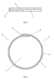
- a sheet 3 to be folded to an electric conductor within a RF waveguide basically comprises a first layer 1 that is made of a plastic foil and a second layer 2 that is made of an electric conductive material such as copper, silver or gold (Fig. 1).
- the plastic foil is a polyethylene foil.
- a foil of plastic forming the first layer 1 is laminated with an electric conductive material forming the second layer 2 in order to get a combined laminated sheet with at least one layer 2 of an electric conductive material and at least one layer 1 of a plastic foil.
- Lamination takes place e.g. by using an endless stripe of a rolled sheet or foil of an electric conductive material such as metal that is glued on an endless stripe of plastic, e.g. polymer foil in an endless manufacturing process.
- the layer of electric conductive material is used as electric conductor with a thickness allowing conducting maximum occurring currents but also considering the skin effect, i.e. having a minimum thickness.
- the polymer foil layer is used as a carrier providing the mechanical strength of the waveguide.
- copper, silver or gold is used as electro conductive material.
- Figure 2 shows how the combined laminated sheet 3 comprising the first 1 and the second layer 2 is folded to a substantially cylindrical conductor 8. Thereby the margin ends 5, 6 of the folded combined laminated sheet 3 are overlapping. By overlapping the margin ends 5, 6 the internal space 7 enclosed by the combined laminated sheet 3 is totally surrounded by an electric conductive material providing a shielding similar to a solid conductor.
- Folding the combined laminated sheet 3 to a substantially cylindrical conductor 8 can take place by enclosing a core of a waveguide.
- This core can comprise other waveguides or electric conductors but can also be of an electric insulating material.
- the margin ends 50, 60 of the combined, laminated sheet 30 are connected with each other by hemming and/or crimping after folding the sheet 30 to a cylindrical conductor 80, in order to avert bulking when bending the waveguide 90.
- a shielding similar to a solid conductor is achieved.
- the thickness of the electric conductive material can be reduced to the required minimum predefined by the skin deepness, because no welding takes place requiring a certain minimum thickness higher than the skin deepness.
- the waveguide 90 shown in Figure 3a) is a RF coaxial cable having an outer cylindrical conductor 81 and an inner cylindrical conductor 82, both manufactured by the same technique according to the invention.
- the waveguide 91 shown in Figure 3b) is a RF coaxial cable having an outer cylindrical conductor 83 and an inner cylindrical conductor 84, both manufactured by the same technique according to the invention.
- the margin ends 51, 61 of the sheet 31 are overlapping without being hemmed and/or crimped after folding the sheet 31.
- the waveguide 92 shown in Figure 3c) is a RF coaxial cable having an outer cylindrical conductor 85 manufactured according to the invention and an inner cylindrical conductor 86 made of solid copper.
- All waveguides 90, 91, 92 shown in Figures 3a), 3b), 3c) further have an internal space 70 totally enclosed by the particular outer cylindrical conductors 81, 83, 85, wherein the space between the inner 82, 84, 86 and the outer cylindrical conductors 81, 83, 85 is filled with a foam material. Furthermore the outer cylindrical conductors 81, 83, 85 are surrounded by a cable sheathing 40. Inside the inner cylindrical conductors 81, 83, a core of polyethylene is arranged.
- the arrangement of the electric conductive layer and the plastic foil preferably depends on the usage of the conductor made of the combined laminated sheet. If the conductor is arranged as an inner-conductor, the electric conductive layer preferably is arranged at the outer surface of the conductor, wherein if the conductor is arranged as an outer-conductor, the electric conductive layer preferably is arranged at the inner surface of the conductor.
- the shielding that is achieved by the conductor 81 in Fig. 3a) is more efficient than the shielding that is achieved by the conductor 83 in Fig. 3b).
- the invention is commercially applicable particularly in the field of production of waveguides and/or transmission lines to be used within networks for electromagnetic data transmission.
Landscapes
- Waveguides (AREA)
- Laminated Bodies (AREA)
- Communication Cables (AREA)
- Manufacturing Of Electric Cables (AREA)
- Insulated Conductors (AREA)
Priority Applications (6)
| Application Number | Priority Date | Filing Date | Title |
|---|---|---|---|
| EP06290148A EP1811596B1 (de) | 2006-01-20 | 2006-01-20 | Hochfrequenz-Wellenleiter mit elektrischem Leiter aus einer mit einer leitfähigen Schicht beschichteten Plastikfolie |
| AT06290148T ATE523920T1 (de) | 2006-01-20 | 2006-01-20 | Hochfrequenz-wellenleiter mit elektrischem leiter aus einer mit einer leitfähigen schicht beschichteten plastikfolie |
| US11/638,487 US7683744B2 (en) | 2006-01-20 | 2006-12-14 | Radio frequency waveguide comprising an electric conductor made of a plastic foil layer laminated with a electric conductive material layer |
| JP2007003056A JP2007195176A (ja) | 2006-01-20 | 2007-01-11 | 導電性材料層を貼り合わされたプラスチックフォイル層で製作された導電体を含む無線周波数導波路 |
| CN200710001991.5A CN101005150B (zh) | 2006-01-20 | 2007-01-16 | 射频波导 |
| JP2012236821A JP5620960B2 (ja) | 2006-01-20 | 2012-10-26 | 導電性材料層を貼り合わされたプラスチックフォイル層で製作された導電体を含む無線周波数導波路 |
Applications Claiming Priority (1)
| Application Number | Priority Date | Filing Date | Title |
|---|---|---|---|
| EP06290148A EP1811596B1 (de) | 2006-01-20 | 2006-01-20 | Hochfrequenz-Wellenleiter mit elektrischem Leiter aus einer mit einer leitfähigen Schicht beschichteten Plastikfolie |
Publications (2)
| Publication Number | Publication Date |
|---|---|
| EP1811596A1 true EP1811596A1 (de) | 2007-07-25 |
| EP1811596B1 EP1811596B1 (de) | 2011-09-07 |
Family
ID=36204342
Family Applications (1)
| Application Number | Title | Priority Date | Filing Date |
|---|---|---|---|
| EP06290148A Expired - Lifetime EP1811596B1 (de) | 2006-01-20 | 2006-01-20 | Hochfrequenz-Wellenleiter mit elektrischem Leiter aus einer mit einer leitfähigen Schicht beschichteten Plastikfolie |
Country Status (5)
| Country | Link |
|---|---|
| US (1) | US7683744B2 (de) |
| EP (1) | EP1811596B1 (de) |
| JP (2) | JP2007195176A (de) |
| CN (1) | CN101005150B (de) |
| AT (1) | ATE523920T1 (de) |
Cited By (1)
| Publication number | Priority date | Publication date | Assignee | Title |
|---|---|---|---|---|
| EP2071588A3 (de) * | 2007-12-12 | 2011-11-23 | Alcatel Lucent | Hochfrequenzübertragungsleitung aus zwei Materialien und das dazugehörige Herstellungsverfahren |
Families Citing this family (13)
| Publication number | Priority date | Publication date | Assignee | Title |
|---|---|---|---|---|
| TWM352783U (en) * | 2008-09-11 | 2009-03-11 | Microelectronics Tech Inc | Water-proof communication apparatus |
| JP5645129B2 (ja) * | 2011-04-01 | 2014-12-24 | 日立金属株式会社 | 高周波同軸ケーブル及びその製造方法 |
| EP2845263B1 (de) * | 2012-05-01 | 2019-09-25 | Nanoton, Inc. | Leitendes medium im hochfrequenzbereich |
| JP6282266B2 (ja) * | 2013-04-03 | 2018-02-21 | ソニーセミコンダクタソリューションズ株式会社 | 導波管、導波管の製造方法、及び、無線伝送システム |
| CN105898908A (zh) * | 2016-06-15 | 2016-08-24 | 成都恩承科技股份有限公司 | 一种微波波导管及其微波加热装置 |
| WO2018067116A1 (en) * | 2016-10-04 | 2018-04-12 | Halliburton Energy Services, Inc. | Parallel plate waveguide within a metal pipe |
| EP3399588B1 (de) | 2017-05-05 | 2022-06-22 | Nokia Solutions and Networks Oy | Verbundsubstrat für einen wellenleiter und verfahren zur herstellung eines verbundsubstrats |
| DE102017220919B4 (de) * | 2017-11-23 | 2025-01-30 | Bizlink Industry Germany Gmbh | Verfahren zum Erzeugen einer selbstschließenden Folienummantelung in einer Kabelanordnung, Kabelanordnung mit einer derartigen Folienummantelung und Formwerkzeug zum Erzeugen einer derartigen Folienummantelung |
| CN108682930B (zh) * | 2018-04-24 | 2024-03-26 | 中天射频电缆有限公司 | 一种端接波导过渡器 |
| US11887944B2 (en) | 2020-06-23 | 2024-01-30 | Intel Corporation | Additive manufacturing for integrated circuit assembly connectors |
| US11895815B2 (en) * | 2020-06-23 | 2024-02-06 | Intel Corporation | Additive manufacturing for integrated circuit assembly cables |
| US11842826B2 (en) | 2020-06-23 | 2023-12-12 | Intel Corporation | Additive manufacturing for integrated circuit assembly connector support structures |
| CN114696053B (zh) * | 2020-12-31 | 2025-11-18 | 江苏俊知技术有限公司 | 毫米波用的圆波导传输线及其制造方法 |
Citations (13)
| Publication number | Priority date | Publication date | Assignee | Title |
|---|---|---|---|---|
| DE2022991A1 (de) | 1970-05-12 | 1971-12-02 | Kabel Metallwerke Ghh | Verfahren zur Herstellung eines elektrischen Leiters |
| DE2056352A1 (de) | 1970-11-17 | 1972-05-25 | Kabel Metallwerke Ghh | Verfahren zur Herstellung eines elektrischen Leiters |
| US3692063A (en) * | 1970-03-17 | 1972-09-19 | Kabel Metallwerke Ghh | Flexible waveguide and method of producing |
| US3720994A (en) * | 1970-11-27 | 1973-03-20 | Kabel Metallwerke Ghh | Method of forming metal tubing |
| GB1470080A (en) * | 1973-07-04 | 1977-04-14 | Cables De Lyon Geoffroy Delore | Waveguides |
| US4071834A (en) * | 1975-06-12 | 1978-01-31 | Les Cables De Lyon S.A. | Helical wave guide |
| US4117260A (en) * | 1977-08-17 | 1978-09-26 | Comul Scope Company | Coaxial drop wire |
| GB1598001A (en) * | 1978-02-27 | 1981-09-16 | Inst Radiotekh Elektron | Method of manufacturing hollow waveguides for transmission of electromagnetic waves and waveguides realised by this method |
| JPS58146104A (ja) * | 1982-02-25 | 1983-08-31 | Sumitomo Electric Ind Ltd | 漏洩同軸ケ−ブルの製造方法 |
| JP2000068732A (ja) * | 1998-08-26 | 2000-03-03 | Hitachi Cable Ltd | 漏洩導波管 |
| JP2000201017A (ja) * | 1998-10-27 | 2000-07-18 | Furukawa Electric Co Ltd:The | 可撓漏洩導波管およびその製造方法 |
| JP2003179415A (ja) * | 2001-12-13 | 2003-06-27 | Mitsubishi Cable Ind Ltd | 漏洩導波管及びその製法 |
| US20030174030A1 (en) | 2002-03-18 | 2003-09-18 | Andrew Corporation | RF cable having clad conductors and method of making same |
Family Cites Families (18)
| Publication number | Priority date | Publication date | Assignee | Title |
|---|---|---|---|---|
| US2783440A (en) * | 1955-01-26 | 1957-02-26 | Lockheed Aircraft Corp | Light weight wave guide construction |
| DE1160048B (de) * | 1962-06-16 | 1963-12-27 | Felten & Guilleaume Carlswerk | Rechteckhohlleiter und Verfahren zu seiner Herstellung |
| US3195079A (en) * | 1963-10-07 | 1965-07-13 | Burton Silverplating | Built up nonmetallic wave guide having metallic coating extending into corner joint and method of making same |
| DE1490801A1 (de) * | 1964-07-18 | 1969-07-17 | Telefunken Patent | Quadratischer Hohlleiter |
| DE1807718A1 (de) * | 1968-11-08 | 1970-05-21 | Telefunken Patent | Mikrowellenhohlleiter |
| JPS4899475U (de) * | 1972-02-25 | 1973-11-24 | ||
| JPS5032579A (de) * | 1973-07-26 | 1975-03-29 | ||
| JPS5126391U (de) * | 1974-08-14 | 1976-02-26 | ||
| DE2841934A1 (de) * | 1978-09-27 | 1980-04-17 | Kabel Metallwerke Ghh | Waermeisoliertes leitungsrohr und verfahren zu seiner herstellung |
| JPS60192508U (ja) * | 1984-05-30 | 1985-12-20 | 三菱電線工業株式会社 | 漏洩同軸ケ−ブル |
| JPS62276904A (ja) * | 1986-02-12 | 1987-12-01 | Hitachi Cable Ltd | 耐火性漏洩同軸ケ−ブル |
| EP0503129A1 (de) * | 1991-03-09 | 1992-09-16 | kabelmetal electro GmbH | Koaxiales elektrisches Hochfrequenzkabel |
| JP3335393B2 (ja) * | 1992-11-12 | 2002-10-15 | 宮崎電線工業株式会社 | 同軸ケーブルの製造方法 |
| JPH0855524A (ja) * | 1994-08-15 | 1996-02-27 | Mitsubishi Cable Ind Ltd | 耐熱形路側通信用同軸ケーブル |
| JP3443784B2 (ja) * | 1995-11-14 | 2003-09-08 | 東京特殊電線株式会社 | 高周波用同軸ケーブルの製造方法 |
| JPH10107515A (ja) * | 1996-09-30 | 1998-04-24 | Hitachi Cable Ltd | 導波管 |
| JP3088998B2 (ja) * | 1997-12-15 | 2000-09-18 | 中島通信機工業株式会社 | メタルケーブル |
| JP2005244759A (ja) * | 2004-02-27 | 2005-09-08 | Mitsubishi Cable Ind Ltd | 漏洩同軸ケーブル及びその製造方法 |
-
2006
- 2006-01-20 EP EP06290148A patent/EP1811596B1/de not_active Expired - Lifetime
- 2006-01-20 AT AT06290148T patent/ATE523920T1/de not_active IP Right Cessation
- 2006-12-14 US US11/638,487 patent/US7683744B2/en not_active Expired - Fee Related
-
2007
- 2007-01-11 JP JP2007003056A patent/JP2007195176A/ja not_active Withdrawn
- 2007-01-16 CN CN200710001991.5A patent/CN101005150B/zh not_active Expired - Fee Related
-
2012
- 2012-10-26 JP JP2012236821A patent/JP5620960B2/ja not_active Expired - Fee Related
Patent Citations (13)
| Publication number | Priority date | Publication date | Assignee | Title |
|---|---|---|---|---|
| US3692063A (en) * | 1970-03-17 | 1972-09-19 | Kabel Metallwerke Ghh | Flexible waveguide and method of producing |
| DE2022991A1 (de) | 1970-05-12 | 1971-12-02 | Kabel Metallwerke Ghh | Verfahren zur Herstellung eines elektrischen Leiters |
| DE2056352A1 (de) | 1970-11-17 | 1972-05-25 | Kabel Metallwerke Ghh | Verfahren zur Herstellung eines elektrischen Leiters |
| US3720994A (en) * | 1970-11-27 | 1973-03-20 | Kabel Metallwerke Ghh | Method of forming metal tubing |
| GB1470080A (en) * | 1973-07-04 | 1977-04-14 | Cables De Lyon Geoffroy Delore | Waveguides |
| US4071834A (en) * | 1975-06-12 | 1978-01-31 | Les Cables De Lyon S.A. | Helical wave guide |
| US4117260A (en) * | 1977-08-17 | 1978-09-26 | Comul Scope Company | Coaxial drop wire |
| GB1598001A (en) * | 1978-02-27 | 1981-09-16 | Inst Radiotekh Elektron | Method of manufacturing hollow waveguides for transmission of electromagnetic waves and waveguides realised by this method |
| JPS58146104A (ja) * | 1982-02-25 | 1983-08-31 | Sumitomo Electric Ind Ltd | 漏洩同軸ケ−ブルの製造方法 |
| JP2000068732A (ja) * | 1998-08-26 | 2000-03-03 | Hitachi Cable Ltd | 漏洩導波管 |
| JP2000201017A (ja) * | 1998-10-27 | 2000-07-18 | Furukawa Electric Co Ltd:The | 可撓漏洩導波管およびその製造方法 |
| JP2003179415A (ja) * | 2001-12-13 | 2003-06-27 | Mitsubishi Cable Ind Ltd | 漏洩導波管及びその製法 |
| US20030174030A1 (en) | 2002-03-18 | 2003-09-18 | Andrew Corporation | RF cable having clad conductors and method of making same |
Non-Patent Citations (4)
| Title |
|---|
| PATENT ABSTRACTS OF JAPAN vol. 007, no. 264 (E - 212) 24 November 1983 (1983-11-24) * |
| PATENT ABSTRACTS OF JAPAN vol. 2000, no. 06 22 September 2000 (2000-09-22) * |
| PATENT ABSTRACTS OF JAPAN vol. 2000, no. 10 17 November 2000 (2000-11-17) * |
| PATENT ABSTRACTS OF JAPAN vol. 2003, no. 10 8 October 2003 (2003-10-08) * |
Cited By (1)
| Publication number | Priority date | Publication date | Assignee | Title |
|---|---|---|---|---|
| EP2071588A3 (de) * | 2007-12-12 | 2011-11-23 | Alcatel Lucent | Hochfrequenzübertragungsleitung aus zwei Materialien und das dazugehörige Herstellungsverfahren |
Also Published As
| Publication number | Publication date |
|---|---|
| US20070171007A1 (en) | 2007-07-26 |
| CN101005150B (zh) | 2011-08-03 |
| JP2013042541A (ja) | 2013-02-28 |
| CN101005150A (zh) | 2007-07-25 |
| JP5620960B2 (ja) | 2014-11-05 |
| US7683744B2 (en) | 2010-03-23 |
| ATE523920T1 (de) | 2011-09-15 |
| JP2007195176A (ja) | 2007-08-02 |
| EP1811596B1 (de) | 2011-09-07 |
Similar Documents
| Publication | Publication Date | Title |
|---|---|---|
| JP5620960B2 (ja) | 導電性材料層を貼り合わされたプラスチックフォイル層で製作された導電体を含む無線周波数導波路 | |
| CN102201276B (zh) | 差分信号电缆、电缆组件以及多对差分信号电缆 | |
| US10306819B2 (en) | Shielded electrical cable | |
| US10373734B2 (en) | Shielded electrical ribbon cable with dielectric spacing | |
| CN104616822B (zh) | 差分信号用电缆、传输电缆及差分信号用电缆的制造方法 | |
| EP3726539A1 (de) | Flachkabel und verfahren zur herstellung eines flachkabels | |
| KR102834291B1 (ko) | 동축 케이블 및 케이블 어셈블리 | |
| JP2010192287A (ja) | 高速伝送用フレキシブルフラット高周波ケーブル端末接続構造及びその製造方法 | |
| CN104756201B (zh) | 微波电缆及制造和使用这种微波电缆的方法 | |
| KR20220120698A (ko) | 다층의 차폐된 접지 케이블 및 관련 방법 | |
| JP7081699B2 (ja) | 同軸ケーブル及びケーブルアセンブリ | |
| JP2020181648A (ja) | 回路モジュールと回路モジュールの製造方法 | |
| CN114171252B (zh) | 同轴电缆以及电缆组件 | |
| EP2232507B1 (de) | Koaxialkabel mit einer röhrenförmigen bimetallischen inneren schicht mit abgewinkelter randverbindung und diesbezügliche verfahren | |
| JP2006302790A (ja) | 同軸ケーブル及び同軸コネクタ | |
| CN214377713U (zh) | 数据线、数据线总成以及电子设备 | |
| WO2011069139A2 (en) | Coaxial cable shielding | |
| JP2010170800A (ja) | 信号伝送線路 |
Legal Events
| Date | Code | Title | Description |
|---|---|---|---|
| PUAI | Public reference made under article 153(3) epc to a published international application that has entered the european phase |
Free format text: ORIGINAL CODE: 0009012 |
|
| 17P | Request for examination filed |
Effective date: 20061018 |
|
| AK | Designated contracting states |
Kind code of ref document: A1 Designated state(s): AT BE BG CH CY CZ DE DK EE ES FI FR GB GR HU IE IS IT LI LT LU LV MC NL PL PT RO SE SI SK TR |
|
| AX | Request for extension of the european patent |
Extension state: AL BA HR MK YU |
|
| AKX | Designation fees paid |
Designated state(s): AT BE BG CH CY CZ DE DK EE ES FI FR GB GR HU IE IS IT LI LT LU LV MC NL PL PT RO SE SI SK TR |
|
| GRAP | Despatch of communication of intention to grant a patent |
Free format text: ORIGINAL CODE: EPIDOSNIGR1 |
|
| GRAS | Grant fee paid |
Free format text: ORIGINAL CODE: EPIDOSNIGR3 |
|
| GRAA | (expected) grant |
Free format text: ORIGINAL CODE: 0009210 |
|
| REG | Reference to a national code |
Ref country code: GB Ref legal event code: FG4D |
|
| REG | Reference to a national code |
Ref country code: CH Ref legal event code: EP |
|
| REG | Reference to a national code |
Ref country code: IE Ref legal event code: FG4D |
|
| REG | Reference to a national code |
Ref country code: DE Ref legal event code: R096 Ref document number: 602006024160 Country of ref document: DE Effective date: 20111103 |
|
| REG | Reference to a national code |
Ref country code: NL Ref legal event code: VDEP Effective date: 20110907 |
|
| PG25 | Lapsed in a contracting state [announced via postgrant information from national office to epo] |
Ref country code: LT Free format text: LAPSE BECAUSE OF FAILURE TO SUBMIT A TRANSLATION OF THE DESCRIPTION OR TO PAY THE FEE WITHIN THE PRESCRIBED TIME-LIMIT Effective date: 20110907 Ref country code: FI Free format text: LAPSE BECAUSE OF FAILURE TO SUBMIT A TRANSLATION OF THE DESCRIPTION OR TO PAY THE FEE WITHIN THE PRESCRIBED TIME-LIMIT Effective date: 20110907 Ref country code: SE Free format text: LAPSE BECAUSE OF FAILURE TO SUBMIT A TRANSLATION OF THE DESCRIPTION OR TO PAY THE FEE WITHIN THE PRESCRIBED TIME-LIMIT Effective date: 20110907 |
|
| RAP2 | Party data changed (patent owner data changed or rights of a patent transferred) |
Owner name: ALCATEL LUCENT |
|
| LTIE | Lt: invalidation of european patent or patent extension |
Effective date: 20110907 |
|
| PG25 | Lapsed in a contracting state [announced via postgrant information from national office to epo] |
Ref country code: AT Free format text: LAPSE BECAUSE OF FAILURE TO SUBMIT A TRANSLATION OF THE DESCRIPTION OR TO PAY THE FEE WITHIN THE PRESCRIBED TIME-LIMIT Effective date: 20110907 Ref country code: GR Free format text: LAPSE BECAUSE OF FAILURE TO SUBMIT A TRANSLATION OF THE DESCRIPTION OR TO PAY THE FEE WITHIN THE PRESCRIBED TIME-LIMIT Effective date: 20111208 Ref country code: CY Free format text: LAPSE BECAUSE OF FAILURE TO SUBMIT A TRANSLATION OF THE DESCRIPTION OR TO PAY THE FEE WITHIN THE PRESCRIBED TIME-LIMIT Effective date: 20110907 Ref country code: LV Free format text: LAPSE BECAUSE OF FAILURE TO SUBMIT A TRANSLATION OF THE DESCRIPTION OR TO PAY THE FEE WITHIN THE PRESCRIBED TIME-LIMIT Effective date: 20110907 Ref country code: SI Free format text: LAPSE BECAUSE OF FAILURE TO SUBMIT A TRANSLATION OF THE DESCRIPTION OR TO PAY THE FEE WITHIN THE PRESCRIBED TIME-LIMIT Effective date: 20110907 |
|
| REG | Reference to a national code |
Ref country code: CH Ref legal event code: PCOW Free format text: ALCATEL LUCENT;3, AVENUE OCTAVE GREARD;75007 PARIS (FR) |
|
| REG | Reference to a national code |
Ref country code: AT Ref legal event code: MK05 Ref document number: 523920 Country of ref document: AT Kind code of ref document: T Effective date: 20110907 |
|
| PG25 | Lapsed in a contracting state [announced via postgrant information from national office to epo] |
Ref country code: BE Free format text: LAPSE BECAUSE OF FAILURE TO SUBMIT A TRANSLATION OF THE DESCRIPTION OR TO PAY THE FEE WITHIN THE PRESCRIBED TIME-LIMIT Effective date: 20110907 |
|
| PG25 | Lapsed in a contracting state [announced via postgrant information from national office to epo] |
Ref country code: IS Free format text: LAPSE BECAUSE OF FAILURE TO SUBMIT A TRANSLATION OF THE DESCRIPTION OR TO PAY THE FEE WITHIN THE PRESCRIBED TIME-LIMIT Effective date: 20120107 Ref country code: SK Free format text: LAPSE BECAUSE OF FAILURE TO SUBMIT A TRANSLATION OF THE DESCRIPTION OR TO PAY THE FEE WITHIN THE PRESCRIBED TIME-LIMIT Effective date: 20110907 Ref country code: CZ Free format text: LAPSE BECAUSE OF FAILURE TO SUBMIT A TRANSLATION OF THE DESCRIPTION OR TO PAY THE FEE WITHIN THE PRESCRIBED TIME-LIMIT Effective date: 20110907 |
|
| PG25 | Lapsed in a contracting state [announced via postgrant information from national office to epo] |
Ref country code: PL Free format text: LAPSE BECAUSE OF FAILURE TO SUBMIT A TRANSLATION OF THE DESCRIPTION OR TO PAY THE FEE WITHIN THE PRESCRIBED TIME-LIMIT Effective date: 20110907 Ref country code: EE Free format text: LAPSE BECAUSE OF FAILURE TO SUBMIT A TRANSLATION OF THE DESCRIPTION OR TO PAY THE FEE WITHIN THE PRESCRIBED TIME-LIMIT Effective date: 20110907 Ref country code: RO Free format text: LAPSE BECAUSE OF FAILURE TO SUBMIT A TRANSLATION OF THE DESCRIPTION OR TO PAY THE FEE WITHIN THE PRESCRIBED TIME-LIMIT Effective date: 20110907 Ref country code: IT Free format text: LAPSE BECAUSE OF FAILURE TO SUBMIT A TRANSLATION OF THE DESCRIPTION OR TO PAY THE FEE WITHIN THE PRESCRIBED TIME-LIMIT Effective date: 20110907 Ref country code: NL Free format text: LAPSE BECAUSE OF FAILURE TO SUBMIT A TRANSLATION OF THE DESCRIPTION OR TO PAY THE FEE WITHIN THE PRESCRIBED TIME-LIMIT Effective date: 20110907 |
|
| PLBE | No opposition filed within time limit |
Free format text: ORIGINAL CODE: 0009261 |
|
| STAA | Information on the status of an ep patent application or granted ep patent |
Free format text: STATUS: NO OPPOSITION FILED WITHIN TIME LIMIT |
|
| PG25 | Lapsed in a contracting state [announced via postgrant information from national office to epo] |
Ref country code: DK Free format text: LAPSE BECAUSE OF FAILURE TO SUBMIT A TRANSLATION OF THE DESCRIPTION OR TO PAY THE FEE WITHIN THE PRESCRIBED TIME-LIMIT Effective date: 20110907 |
|
| 26N | No opposition filed |
Effective date: 20120611 |
|
| PG25 | Lapsed in a contracting state [announced via postgrant information from national office to epo] |
Ref country code: MC Free format text: LAPSE BECAUSE OF NON-PAYMENT OF DUE FEES Effective date: 20120131 |
|
| REG | Reference to a national code |
Ref country code: CH Ref legal event code: PL |
|
| REG | Reference to a national code |
Ref country code: DE Ref legal event code: R097 Ref document number: 602006024160 Country of ref document: DE Effective date: 20120611 |
|
| REG | Reference to a national code |
Ref country code: IE Ref legal event code: MM4A |
|
| PG25 | Lapsed in a contracting state [announced via postgrant information from national office to epo] |
Ref country code: LI Free format text: LAPSE BECAUSE OF NON-PAYMENT OF DUE FEES Effective date: 20120131 Ref country code: CH Free format text: LAPSE BECAUSE OF NON-PAYMENT OF DUE FEES Effective date: 20120131 |
|
| PG25 | Lapsed in a contracting state [announced via postgrant information from national office to epo] |
Ref country code: IE Free format text: LAPSE BECAUSE OF NON-PAYMENT OF DUE FEES Effective date: 20120120 |
|
| PG25 | Lapsed in a contracting state [announced via postgrant information from national office to epo] |
Ref country code: ES Free format text: LAPSE BECAUSE OF FAILURE TO SUBMIT A TRANSLATION OF THE DESCRIPTION OR TO PAY THE FEE WITHIN THE PRESCRIBED TIME-LIMIT Effective date: 20111218 |
|
| PG25 | Lapsed in a contracting state [announced via postgrant information from national office to epo] |
Ref country code: BG Free format text: LAPSE BECAUSE OF FAILURE TO SUBMIT A TRANSLATION OF THE DESCRIPTION OR TO PAY THE FEE WITHIN THE PRESCRIBED TIME-LIMIT Effective date: 20111207 |
|
| REG | Reference to a national code |
Ref country code: GB Ref legal event code: 732E Free format text: REGISTERED BETWEEN 20130926 AND 20131002 |
|
| REG | Reference to a national code |
Ref country code: FR Ref legal event code: GC Effective date: 20131018 |
|
| PG25 | Lapsed in a contracting state [announced via postgrant information from national office to epo] |
Ref country code: TR Free format text: LAPSE BECAUSE OF FAILURE TO SUBMIT A TRANSLATION OF THE DESCRIPTION OR TO PAY THE FEE WITHIN THE PRESCRIBED TIME-LIMIT Effective date: 20110907 |
|
| PG25 | Lapsed in a contracting state [announced via postgrant information from national office to epo] |
Ref country code: LU Free format text: LAPSE BECAUSE OF NON-PAYMENT OF DUE FEES Effective date: 20120120 |
|
| PG25 | Lapsed in a contracting state [announced via postgrant information from national office to epo] |
Ref country code: HU Free format text: LAPSE BECAUSE OF FAILURE TO SUBMIT A TRANSLATION OF THE DESCRIPTION OR TO PAY THE FEE WITHIN THE PRESCRIBED TIME-LIMIT Effective date: 20060120 Ref country code: PT Free format text: LAPSE BECAUSE OF FAILURE TO SUBMIT A TRANSLATION OF THE DESCRIPTION OR TO PAY THE FEE WITHIN THE PRESCRIBED TIME-LIMIT Effective date: 20110907 |
|
| REG | Reference to a national code |
Ref country code: FR Ref legal event code: RG Effective date: 20141016 |
|
| REG | Reference to a national code |
Ref country code: FR Ref legal event code: PLFP Year of fee payment: 10 |
|
| REG | Reference to a national code |
Ref country code: FR Ref legal event code: PLFP Year of fee payment: 11 |
|
| REG | Reference to a national code |
Ref country code: FR Ref legal event code: PLFP Year of fee payment: 12 |
|
| PGFP | Annual fee paid to national office [announced via postgrant information from national office to epo] |
Ref country code: FR Payment date: 20170120 Year of fee payment: 12 Ref country code: DE Payment date: 20170120 Year of fee payment: 12 |
|
| PGFP | Annual fee paid to national office [announced via postgrant information from national office to epo] |
Ref country code: GB Payment date: 20170119 Year of fee payment: 12 |
|
| REG | Reference to a national code |
Ref country code: DE Ref legal event code: R119 Ref document number: 602006024160 Country of ref document: DE |
|
| GBPC | Gb: european patent ceased through non-payment of renewal fee |
Effective date: 20180120 |
|
| PG25 | Lapsed in a contracting state [announced via postgrant information from national office to epo] |
Ref country code: FR Free format text: LAPSE BECAUSE OF NON-PAYMENT OF DUE FEES Effective date: 20180131 Ref country code: DE Free format text: LAPSE BECAUSE OF NON-PAYMENT OF DUE FEES Effective date: 20180801 |
|
| REG | Reference to a national code |
Ref country code: FR Ref legal event code: ST Effective date: 20180928 |
|
| PG25 | Lapsed in a contracting state [announced via postgrant information from national office to epo] |
Ref country code: GB Free format text: LAPSE BECAUSE OF NON-PAYMENT OF DUE FEES Effective date: 20180120 |