EP1814156A2 - Flachbildschirm-Röntgenbildgebungsvorrichtung mit amorphem Selen für Tomosynthese und statische Bildgebung - Google Patents
Flachbildschirm-Röntgenbildgebungsvorrichtung mit amorphem Selen für Tomosynthese und statische Bildgebung Download PDFInfo
- Publication number
- EP1814156A2 EP1814156A2 EP07250338A EP07250338A EP1814156A2 EP 1814156 A2 EP1814156 A2 EP 1814156A2 EP 07250338 A EP07250338 A EP 07250338A EP 07250338 A EP07250338 A EP 07250338A EP 1814156 A2 EP1814156 A2 EP 1814156A2
- Authority
- EP
- European Patent Office
- Prior art keywords
- imager
- charge
- top electrode
- layer
- angstroms
- Prior art date
- Legal status (The legal status is an assumption and is not a legal conclusion. Google has not performed a legal analysis and makes no representation as to the accuracy of the status listed.)
- Ceased
Links
Images


Classifications
-
- H—ELECTRICITY
- H10—SEMICONDUCTOR DEVICES; ELECTRIC SOLID-STATE DEVICES NOT OTHERWISE PROVIDED FOR
- H10F—INORGANIC SEMICONDUCTOR DEVICES SENSITIVE TO INFRARED RADIATION, LIGHT, ELECTROMAGNETIC RADIATION OF SHORTER WAVELENGTH OR CORPUSCULAR RADIATION
- H10F39/00—Integrated devices, or assemblies of multiple devices, comprising at least one element covered by group H10F30/00, e.g. radiation detectors comprising photodiode arrays
- H10F39/10—Integrated devices
- H10F39/12—Image sensors
- H10F39/191—Photoconductor image sensors
- H10F39/195—X-ray, gamma-ray or corpuscular radiation imagers
-
- H—ELECTRICITY
- H10—SEMICONDUCTOR DEVICES; ELECTRIC SOLID-STATE DEVICES NOT OTHERWISE PROVIDED FOR
- H10F—INORGANIC SEMICONDUCTOR DEVICES SENSITIVE TO INFRARED RADIATION, LIGHT, ELECTROMAGNETIC RADIATION OF SHORTER WAVELENGTH OR CORPUSCULAR RADIATION
- H10F30/00—Individual radiation-sensitive semiconductor devices in which radiation controls the flow of current through the devices, e.g. photodetectors
- H10F30/20—Individual radiation-sensitive semiconductor devices in which radiation controls the flow of current through the devices, e.g. photodetectors the devices having potential barriers, e.g. phototransistors
- H10F30/29—Individual radiation-sensitive semiconductor devices in which radiation controls the flow of current through the devices, e.g. photodetectors the devices having potential barriers, e.g. phototransistors the devices being sensitive to radiation having very short wavelengths, e.g. X-rays, gamma-rays or corpuscular radiation
Definitions
- This patent specification is in the field of radiography and pertains more specifically to x-ray imaging using a digital, flat panel x-ray imager.
- DRC Direct Radiography Corporation of Newark, DE.
- the DRC imager is used in mammography systems that have been available for more than a year in this country from Lorad Corporation of Danbury, CT (“Lorad”).
- the charge generator material directly converts x-rays into pairs of electrons and holes and, under an applied electrical field, the holes and electrons migrate to respective electrodes with very little lateral loss to neighboring pixels.
- Direct conversion is believed to offer better spatial resolution and other advantages over indirect conversion panels, in which x-rays cause scintillation in a material such as cesium iodide and the resulting light energy is detected.
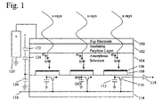
- a direct conversion flat panel imager of the type referred to above is illustrated in principle but not to scale in Fig. 1. It comprises a top electrode 100, a charge barrier layer 102 (typically made of Parylene) separating the top electrode from an amorphous selenium-based charge generator layer 104, an electron blocking layer 106 patterned into a two-dimensional pixel array, a charge collection electrode 108 that also is patterned into a pixel array, a thin-film transistor (“TFT”) array comprising respective transistors 110 coupled to the charge collection electrode and to respective signal storage capacitors 112, a substrate 114 typically made of glass, a gate pulse line 116 that enables (turns ON) the transistors to deliver to charge amplifiers 118 the charges collected at the respective storage capacitors, an a programmable high voltage power supply 120.
- TFT thin-film transistor
- the illustrated equivalent capacitor circuit for a pixel comprises a capacitor 122 representing capacitance across the charge barrier layer, a capacitor 124 representing capacitance across the charge generator layer, and a capacitor 126 representing capacitance of the charge storage capacitor for the pixel.
- One of the functions of the charge barrier layer is protection of the thin-film transistors, which can suffer breakdown damage if the charge stored in the charge storage capacitors becomes too high, e.g. when a capacitor stores charges generated at a region of the charge generating layer that receives x-rays that have not been attenuated by the object being imaged. For example, in mammography the corners of the flat panel imager typically are outside the breast outline and can receive much more radiation than the part of the imager under the breast.
- the charge barrier layer protects such transistors by collecting charges that gradually reduce the electrical field in the appropriate portions of the charge generator layer, and thus reduce the amount of charge that would otherwise collect at the pertinent charge collection capacitors.
- the charge barrier layer thus contributes to meeting one of the challenges in flat panel detectors, namely, breakdown protection of the thin-film transistors.
- Another challenge is ghosting (remnants of one or more previous images) due to the time it takes to dissipate charges collected in the imager from previous x-ray exposures.
- ghosting suppresses the ghosting to an acceptable level. They include charge erasing by exposure to visible light between x-ray exposures and various ways to manipulate the bias potential of electrodes between x-ray exposures. The time needed to attend to ghosting makes it difficult to take images in rapid succession, such as for fluoroscopy or tomosynthesis.
- U.S. Patent No. 6,353,229 proposes to achieve high voltage protection "by setting the high voltage biasing electrode to a negative potential and the TFT "off' gate voltage to a predetermined negative value such that the TFT is essentially non-conductive.”
- the patent recognizes that "there will always be some TFT leakage” but states that "the negative 'off' voltage may be adjusted so as to minimize the same and render the TFT essentially non-conductive.” See column 2, lines 49-61.
- the new approach includes placing a layer of non-insulating organic material between a top electrode and a selenium-based charge generator layer serving to directly convert x-rays to electrical charges, and may intentionally use leakage current of the TFT array transistors for protection.
- the leakage current characteristics of the TFT array transistors may provide an operating regime in which the leakage current may be relatively low for pixels that measure radiation within the typical range expected for the object being imaged but the leakage current may be sufficiently high to avoid transistor breakdown for pixels that receive more radiation, e.g.
- the TFT leakage current regime may provide breakdown protection despite the absence of a charge barrier layer between the top electrode and the charge generator layer designed to protect from high voltage TFT breakdown.
- a layer of non-insulating organic material may be deposited or otherwise formed directly on the selenium-based layer.
- a top metal electrode may be deposited or otherwise formed directly on the non-insulating organic material. No charge blocking or insulating layer need be deliberately formed between the top electrode and the charge generator layer.
- the leakage current of the thin-film transistors may rise at a relatively low rate with voltage at the transistors up to a selected range but may rise much more steeply with voltage at the transistors above that range.
- the leakage current rises at a low rate up to transistor voltage in the range of 20-25 volts but rises much more steeply with voltage above that range. At higher voltage, the steeply rising leakage current provides built-in protection against transistor breakdown.
- the range of 20-25 volts is only an example, and other ranges may be appropriate to accomplish protection in the case of differently structured TFT array transistors or imagers.
- the top electrode may be formed directly on the selenium-based charge generator layer.
- a non-limiting example of an imager incorporating the teachings of this patent specification comprises a top metal electrode 100 deposited or otherwise formed directly on an electronically non-insulating organic material 202.
- the non-insulating organic material 202 may be deposited or otherwise formed directly on, an upper surface of an amorphous selenium-based charge generator layer 104.
- a charge collection electrode 108 is patterned into a two-dimensional array of pixel electrodes that are under charge generator layer 104 or are embedded at a bottom surfaces thereof.
- An electron blocking layer 106 may cover pixel electrodes 108 (also called charge collection electrode).
- a read-out circuit is interposed between charge generator layer 104 and a substrate 114, and comprises respective signal storage capacitors 112 coupled electrically with the pixel electrodes and a thin-film transistor (TFT) array comprising respective gating transistors 110 coupled electrically with the junctions between the pixel electrodes and the signal storage capacitors.
- Transistors 110 are normally in an OFF state but can be enabled (turned ON) by a gating signal delivered over gate pulse line 116, to thereby deliver charge accumulated in signal storage capacitors to a charge amplifier 118.
- a programmable high voltage power supply 120 applies a positive potential to top electrode 100 relative to ground and to grounded signal storage capacitors 112, to thereby induce an electrical field in charge generator layer 104.
- Additional electrical fields can be generated as well, for example by forming and appropriately biasing special electrodes that extend into the underside of charge generator layer 104, between adjacent charger collector electrodes 108.
- Fig. 1 is not to scale, and omits well known components of an imaging panel, such as a protective layer over top electrode 100 (e.g. Parylene passivation over a top electrode, or any protective layer over the top electrode) and various other mechanical or electrical components that are a part of the imaging panel that has been available from DRC and used by Lorad for mammography and has 3584 by 4096 square pixels at 70 microns pitch over an active area of about 25 by 29 cm.
- the charge generator layer may be about 200 microns thick and may be thermally stabilized by controlled amounts of dopants. A voltage of about 1,000 volts across the charge generator layer may be used, resulting in an electric field of about 5 volts per micron thickness.
- additional gate pulse lines G 2 ... G n that are similar to line 116 (G 1 ) but serve other rows of transistors 110
- a gate driver 300 directed by a controller 302 to selectively enable transistors 110 in the respective rows
- column readout lines D 1 ... D m that feed the outputs of transistors 110 in respective columns to sample-and-hold (S/H) circuits 304.
- a multiplexer 306 takes the output of circuits 304 and feeds analog-to-digital converters (ADC) 308, also controlled by controller 302.
- ADC analog-to-digital converters
- Digitized pixel values from ADC 308 are delivered to serial data port 310 and then to an image buffer, from which they can be taken for appropriate processing into image data for display, storage, transmission, etc.
- the pixel charges can be read out individually, or several pixels (e.g. an array of 2 by 2 pixels) can be binned into a single sample for higher reading speed at the expense of spatial resolution.
- the panel can be operated in a static mode for screening mammography, for example at a 28 kVp, MO/MO spectrum provided by an x-ray generator from Lorad designated M4, with an image cycle of 30 seconds and at a source-detector distance of 65 cm.
- an exposure range of 1 to 16 mR can be used, which subsumes the typical dose of 1-10 mR for breast cancer screening.
- the panel can be operated in a dynamic, tomosynthesis mode, for example using a 28 kVp, Mo/Rh spectrum, with an image cycle of 0.5 or 1.0 seconds and 2x2 pixel binning, and at exposure range of about 0.5-1.5 mR per image, i.e. at a dose range per image of about a factor of 10 less than for the static, screening mode so that about 10 or 11 images can be taken in dynamic, tomosynthesis mode in one sweep of stop-and-expose imaging.
- the non-insulating organic layer (202 of Fig. 2) may be a hole-blocking layer and may prevent positive charge from traveling from the power source 120 and the top electrode 100 to the charge generating layer 104. However, the non-insulating organic layer 202 may permit negative charge to flow from the charge generating layer 104 to the top electrode 100. The non-insulating organic layer 202 may therefore prevent hole injection at the top metal-semiconductor interface and therefore decrease the detector dark current (signal detected in the absence of x-rays). Decreasing dark current may increase the dynamic range of the detector and decrease the noise in the image.
- the non-insulating organic layer may be, for example, an organic semiconductor.
- organic semiconductors include: phthalocyanines (Pc), oxidiazols and oxazoles, polythiophenes, pentacenes, oligothiophenes, TCNQ (tetracyanoquinodimethane), TDEA (tetrakis demethylaminoethane), tetracarboxylic dianhydride, fullerenes (C60, C70), arylalkanes, arylamines, polysilylenes, polygermanes, PVK (poly-vinylcarbazole) and related compounds, and pyrazolines.
- the listed organic semiconductors are given as examples and are not offered as an exclusive list of all non-insulating organic layers that may be used according to embodiments of the present invention.
- the non-insulating organic layer may be of a thickness within the range of 50 Angstroms to 10,000 Angstroms. It is believed that a thickness within this range would be effective.
- the top-electrode 100 may be directly in contact with the charge generating layer 104.
- Both embodiments of the present invention may have similar characteristics and advantages over the prior art approach as shown in Fig. 1.
- both embodiments may allow for tomographic imaging in the range of, for example, 30 frames per second.
- both embodiments of the present invention may utilize the imager circuitry shown in Fig. 3.
- Fig. 5 illustrates leakage current characteristics of a thin-film transistor 110 that are particularly important for the operation of the imager of Figs. 3 and 4.
- the voltage at the transistor drain 110a is less than about 20 volts, or at least less than somewhere in the range of about 20-25 volts
- the leakage current of the transistor rises at a relatively low rate.
- the leakage current rises at a significantly higher rate (more steeply) with rise in the voltage at 112a above the range of about 20-25 volts.
- the inflection point between low and high rates of leakage current rise is closer to 20 volts than to 25 volts.
- the rise above the inflection point is progressively steeper. While the exact point of inflection or range in which the point of inflection occurs may vary depending on the details of a particular TFT array, the important feature is that the leakage increase at a sufficiently high rate above a voltage range appropriate for a particular use of an imager panel to avoid voltage breakdown of (or overvoltage damage to) the transistors.
- the leakage current of each of the transistors is less than 2 pA at transistor voltage of 20 volts and more than 20 pA at transistor voltage of 35 volts.
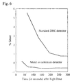
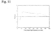
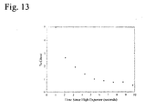
- Fig. 6 compares ghosting of an imaging panel currently sold by Direct Radiography Corporation (standard DRC detector, as illustrated in Fig. 1) with an otherwise similar panel of the type illustrated in Fig. 4 (metal on selenium detector).
- standard DRC detector has a charge barrier layer (layer 102 in Fig.
- the detector while in the detector according to embodiments of the present invention may have either the top electrode 100 in direct contact with the charge generator layer 104 or a non-insulating organic layer 202 between the top electrode 100 and the charge generator layer 104.
- the three panels can be otherwise identical, with identical TFT arrays.
- transistors 110 according to the embodiment of the present invention showen in Figs. 2 and 4 may operate in a different regime, in which they are allowed to extend the voltage at drain 1 l0a into a range that the insulating charge barrier layer 102 in the standard DRC detector was designed to prevent.
- the low ghosting that detectors of embodiments of the present invention exhibit may allow for rapid imaging as compared with the standard DRC detector of Fig. 1. While the x-ray imagers of Figs. 2-4 may use technology for erasing ghost images between x-ray exposures that is the same or similar to those used in the imagers currently sold by Direct Radiology Corporation, in the alternative it may be possible to use the imager of Figs. 2-4 without such erasing.
- the top electrode 100 typically is elemental metal or an alloy or inorganic oxide such as Indium-Tin Oxide (ITO), but an organic conductor may be used instead.
- the material of top electrode 100 preferably has a lower work function than the charge generator layer 104.
- top electrode 100 is made of a material that would allow a free flow of negative charge from the charge generator layer 104 to the non-insulating organic layer 202 into electrode 100 while inhibiting the injection of positive charge from electrode 100 to the non-insulating organic layer 202 into charge generating layer 104.
- the material of top electrode 100 has the following characteristics: work function ⁇ 4.0 electron volt; electrical resistivity ⁇ 55 ⁇ cm; atomic number ⁇ 60.
- top electrode 100 preferably is chemically stable when in contact with the non-insulating organic layer 202 or charge generating layer 104, is not flammable in solid form and is neither explosive nor corrosive, is not too toxic or carcinogenic or radioactive, and allows the formation of top electrode 100 by a deposition or other process compatible with forming the remaining structure of the imaging panel.
- Chromium (Cr) is believed to be an example of a suitable material that meets the criteria set forth above, for example in thickness within the range of about 50 to about 10,000 Angstroms, although other thicknesses also may be suitable.
- top electrode be too thick or too thin may reduce structural integrity during manufacture and/or operation and/or increase x-ray absorption level to an unacceptable level. Therefore selecting an optimal top electrode thickness is beneficial.
- ITO and Al in elemental form or as the predominant metal in an alloy with each other or with other elements also are believed to be examples of suitable materials.
- Another consideration is thermal expansion compatibility with selenium, which may impose conditions on the composition, thickness, or formation technology of the top electrode.
- x-ray imaging panel may be surprising given common assumptions in x-ray imaging technology. For example, in mammography uses of the prior art panel illustrated in Fig. 1 that had been commercially available, it had been believed that without a charge barrier layer 102 such a high amount of charge would accumulate at the individual signal storage capacitors 112 that the capacitor voltage would rise to a level sufficiently high to damage the dielectric in the capacitor and/or the channel in the thin film transistor 110, leading to permanent damage of the imaging panel.
- One calculation assumes that the leakage current is zero, and estimates that under mammography x-ray energies the imaging panel is accumulating 4.58x10 -15 Coulomb per mR per pixel.
- the maximum x-ray exposure rate is 5R/second, then the maximum accumulated charge at capacitor 112 is 2.3x10 -11 Coulomb in 1 second. This theoretical calculation leads to a voltage of 34.7 volts across signal storage capacitor 112. In practice, in the case of a large and dense breast, the exposure rate is closer to 3 R/second. While this is the estimate assuming there is no leakage current, actual measurements of the TFT in the current mammography imaging panels (Fig. 1) supplied by DRC indicate a rapidly increasing drain-to-source leakage current with increasing voltage over about 20-25 volts. At about 30 volts at the drain, the leakage current is interpolated to be 24 pA, just enough to leak away excess charge as the signal storage capacitor potential roses over 25 volts. This rapidly rising leakage current thus becomes a self-protecting mechanism, which in turn allows dispensing with a charge barrier layer such as 102 (Fig. 1) and its ghosting effects.
- a charge barrier layer such as 102 (Fig. 1) and its ghosting effects.
Landscapes
- Solid State Image Pick-Up Elements (AREA)
- Measurement Of Radiation (AREA)
- Apparatus For Radiation Diagnosis (AREA)
Applications Claiming Priority (1)
| Application Number | Priority Date | Filing Date | Title |
|---|---|---|---|
| US11/341,925 US7233005B2 (en) | 2005-02-16 | 2006-01-27 | Amorphous selenium flat panel x-ray imager for tomosynthesis and static imaging |
Publications (2)
| Publication Number | Publication Date |
|---|---|
| EP1814156A2 true EP1814156A2 (de) | 2007-08-01 |
| EP1814156A3 EP1814156A3 (de) | 2008-11-05 |
Family
ID=37964045
Family Applications (1)
| Application Number | Title | Priority Date | Filing Date |
|---|---|---|---|
| EP07250338A Ceased EP1814156A3 (de) | 2006-01-27 | 2007-01-26 | Flachbildschirm-Röntgenbildgebungsvorrichtung mit amorphem Selen für Tomosynthese und statische Bildgebung |
Country Status (3)
| Country | Link |
|---|---|
| US (1) | US7233005B2 (de) |
| EP (1) | EP1814156A3 (de) |
| JP (1) | JP5566566B2 (de) |
Families Citing this family (14)
| Publication number | Priority date | Publication date | Assignee | Title |
|---|---|---|---|---|
| US7233005B2 (en) * | 2005-02-16 | 2007-06-19 | Hologic, Inc. | Amorphous selenium flat panel x-ray imager for tomosynthesis and static imaging |
| US7304308B2 (en) * | 2005-02-16 | 2007-12-04 | Hologic, Inc. | Amorphous selenium flat panel x-ray imager for tomosynthesis and static imaging |
| US7928401B2 (en) * | 2006-06-14 | 2011-04-19 | Fujifilm Corporation | Radiation detecting system |
| US20090080602A1 (en) * | 2006-08-03 | 2009-03-26 | Kenneth Brooks | Dedicated breast radiation imaging/therapy system |
| US8324582B2 (en) * | 2009-07-16 | 2012-12-04 | Lee Denny L | Direct conversion X-ray imaging device with strip electrodes |
| JP5448643B2 (ja) * | 2009-08-26 | 2014-03-19 | キヤノン株式会社 | 撮像システム、その画像処理方法及びそのプログラム |
| WO2013002326A1 (ja) | 2011-06-30 | 2013-01-03 | 富士フイルム株式会社 | 放射線画像撮影システム |
| TWI461724B (zh) * | 2011-08-02 | 2014-11-21 | Vieworks Co Ltd | 用於輻射成像偵知器的組合物及具有該組合物之輻射成像偵知器 |
| WO2014092001A1 (ja) | 2012-12-10 | 2014-06-19 | 富士フイルム株式会社 | 放射線検出装置 |
| CN105093256B (zh) * | 2015-06-29 | 2017-12-01 | 京东方科技集团股份有限公司 | 一种射线检测基板及其制造方法和射线探测器 |
| US10139500B2 (en) | 2015-10-14 | 2018-11-27 | Shenzhen Xpectvision Technology Co., Ltd. | Semiconductor X-ray detector capable of dark current correction |
| US10353083B2 (en) * | 2017-09-12 | 2019-07-16 | Palo Alto Research Center Incorporated | Monolithic digital x-ray detector stack with energy resolution |
| US10608041B2 (en) * | 2018-04-12 | 2020-03-31 | Palo Alto Research Center Incorporated | Bendable x-ray detector with TFT backplane in the neutral plane |
| US10825855B2 (en) | 2018-12-13 | 2020-11-03 | Palo Alto Research Center Incorporated | Flexible x-ray sensor with integrated strain sensor |
Citations (1)
| Publication number | Priority date | Publication date | Assignee | Title |
|---|---|---|---|---|
| WO2002061456A2 (en) | 2000-11-10 | 2002-08-08 | Hologic, Inc. | Photoconductive imaging panel with externally controlled conductivity |
Family Cites Families (22)
| Publication number | Priority date | Publication date | Assignee | Title |
|---|---|---|---|---|
| DE4002429A1 (de) * | 1990-01-27 | 1991-08-01 | Philips Patentverwaltung | Sensormatrix |
| DE4002431A1 (de) * | 1990-01-27 | 1991-08-01 | Philips Patentverwaltung | Sensormatrix |
| US5198673A (en) * | 1992-01-23 | 1993-03-30 | General Electric Company | Radiation image detector with optical gain selenium photosensors |
| US5254480A (en) * | 1992-02-20 | 1993-10-19 | Minnesota Mining And Manufacturing Company | Process for producing a large area solid state radiation detector |
| DE4227096A1 (de) * | 1992-08-17 | 1994-02-24 | Philips Patentverwaltung | Röntgenbilddetektor |
| US5319206A (en) * | 1992-12-16 | 1994-06-07 | E. I. Du Pont De Nemours And Company | Method and apparatus for acquiring an X-ray image using a solid state device |
| US5436101A (en) * | 1993-08-20 | 1995-07-25 | Xerox Corporation | Negative charging selenium photoreceptor |
| JP3066944B2 (ja) * | 1993-12-27 | 2000-07-17 | キヤノン株式会社 | 光電変換装置、その駆動方法及びそれを有するシステム |
| GB9414639D0 (en) * | 1994-07-20 | 1994-09-07 | Philips Electronics Uk Ltd | An image detector |
| JP3457676B2 (ja) * | 1994-07-27 | 2003-10-20 | リットン システムズ カナダ リミテッド | 放射線像形成パネル |
| JPH11504761A (ja) | 1995-01-19 | 1999-04-27 | リットン システムズ カナダ リミテッド | フラットパネル画像素子 |
| US5528043A (en) * | 1995-04-21 | 1996-06-18 | Thermotrex Corporation | X-ray image sensor |
| US5852296A (en) * | 1996-06-21 | 1998-12-22 | Kabushiki Kaisha Toshiba | X-ray imaging apparatus |
| CA2184667C (en) * | 1996-09-03 | 2000-06-20 | Bradley Trent Polischuk | Multilayer plate for x-ray imaging and method of producing same |
| CA2242743C (en) * | 1998-07-08 | 2002-12-17 | Ftni Inc. | Direct conversion digital x-ray detector with inherent high voltage protection for static and dynamic imaging |
| US6243441B1 (en) * | 1999-07-13 | 2001-06-05 | Edge Medical Devices | Active matrix detector for X-ray imaging |
| JP2001249181A (ja) * | 2000-03-06 | 2001-09-14 | Fuji Photo Film Co Ltd | 固体センサおよび放射線画像読取装置 |
| JP2001281344A (ja) * | 2000-03-30 | 2001-10-10 | Fuji Photo Film Co Ltd | 固体センサおよび放射線画像読取装置 |
| JP2001281345A (ja) * | 2000-03-31 | 2001-10-10 | Fuji Photo Film Co Ltd | エネルギー線検出装置およびその温度調整方法 |
| US6855935B2 (en) * | 2000-03-31 | 2005-02-15 | Canon Kabushiki Kaisha | Electromagnetic wave detector |
| US7233005B2 (en) * | 2005-02-16 | 2007-06-19 | Hologic, Inc. | Amorphous selenium flat panel x-ray imager for tomosynthesis and static imaging |
| US7122803B2 (en) * | 2005-02-16 | 2006-10-17 | Hologic, Inc. | Amorphous selenium flat panel x-ray imager for tomosynthesis and static imaging |
-
2006
- 2006-01-27 US US11/341,925 patent/US7233005B2/en not_active Expired - Lifetime
-
2007
- 2007-01-25 JP JP2007014699A patent/JP5566566B2/ja not_active Expired - Fee Related
- 2007-01-26 EP EP07250338A patent/EP1814156A3/de not_active Ceased
Patent Citations (1)
| Publication number | Priority date | Publication date | Assignee | Title |
|---|---|---|---|---|
| WO2002061456A2 (en) | 2000-11-10 | 2002-08-08 | Hologic, Inc. | Photoconductive imaging panel with externally controlled conductivity |
Non-Patent Citations (1)
| Title |
|---|
| WAKIZAKA D ET AL: "Hole transport in conducting ultrathin films of PEDOT/PSS prepared by layer-by-layer deposition technique", POLYMER, ELSEVIER SCIENCE PUBLISHERS B.V, GB, vol. 45, no. 25, 1 November 2004 (2004-11-01), pages 8561 - 8565, XP004648679, ISSN: 0032-3861, DOI: 10.1016/J.POLYMER.2004.10.007 * |
Also Published As
| Publication number | Publication date |
|---|---|
| JP5566566B2 (ja) | 2014-08-06 |
| US7233005B2 (en) | 2007-06-19 |
| JP2007199065A (ja) | 2007-08-09 |
| EP1814156A3 (de) | 2008-11-05 |
| US20060180768A1 (en) | 2006-08-17 |
Similar Documents
| Publication | Publication Date | Title |
|---|---|---|
| EP1850388A2 (de) | Flachbildschirm-Röntgenbildgebungsvorrichtung mit amorphem Selen für Tomosynthese und statische Bildgebung | |
| EP1814156A2 (de) | Flachbildschirm-Röntgenbildgebungsvorrichtung mit amorphem Selen für Tomosynthese und statische Bildgebung | |
| Kasap et al. | Direct-conversion flat-panel X-ray image sensors for digital radiography | |
| Street et al. | Comparison of PbI 2 and HgI 2 for direct detection active matrix x-ray image sensors | |
| Kabir et al. | Photoconductors for x-ray image detectors | |
| US7122803B2 (en) | Amorphous selenium flat panel x-ray imager for tomosynthesis and static imaging | |
| CA2669678C (en) | Photodetector/imaging device with avalanche gain | |
| Choquette et al. | Direct selenium x-ray detector for fluoroscopy, R&F, and radiography | |
| CA2242743C (en) | Direct conversion digital x-ray detector with inherent high voltage protection for static and dynamic imaging | |
| US8735839B2 (en) | Pastes for photoelectric conversion layers of X-ray detectors, X-ray detectors and methods of manufacturing the same | |
| Street et al. | X-ray imaging using lead iodide as a semiconductor detector | |
| US20080203336A1 (en) | Radiation image detector | |
| US8415662B2 (en) | Radiation detector having a plurality of amorphous selenium layers | |
| CN101546780A (zh) | 辐射检测器 | |
| Street et al. | Large-area x-ray image sensing using a Pbl2 photoconductor | |
| Street et al. | High-resolution direct-detection X-ray imagers | |
| Street et al. | Approaching the theoretical x-ray sensitivity with Hgl2 direct detection image sensors | |
| Kabir | Basic principles of solid-state X-ray radiation detector operation | |
| Scheuermann et al. | Low dose digital X-ray imaging with avalanche amorphous selenium | |
| Zhao et al. | Detectors for tomosynthesis | |
| Kim et al. | Quantitative evaluation of mercuric iodide thick film for x-ray imaging device | |
| Lee et al. | Direct-conversion x-ray imaging detector improvements and observations | |
| Hunter et al. | High-resolution (20 cycles/mm) digital x-ray mammography using amorphous selenium directly coupled to CCD readout devices | |
| Lee et al. | Removal of trapped charge in selenium detectors | |
| Cha et al. | Quantitative evaluation of mercuric Iodide and Selenium for X-ray imaging device |
Legal Events
| Date | Code | Title | Description |
|---|---|---|---|
| PUAI | Public reference made under article 153(3) epc to a published international application that has entered the european phase |
Free format text: ORIGINAL CODE: 0009012 |
|
| AK | Designated contracting states |
Kind code of ref document: A2 Designated state(s): AT BE BG CH CY CZ DE DK EE ES FI FR GB GR HU IE IS IT LI LT LU LV MC NL PL PT RO SE SI SK TR |
|
| AX | Request for extension of the european patent |
Extension state: AL BA HR MK YU |
|
| PUAL | Search report despatched |
Free format text: ORIGINAL CODE: 0009013 |
|
| AK | Designated contracting states |
Kind code of ref document: A3 Designated state(s): AT BE BG CH CY CZ DE DK EE ES FI FR GB GR HU IE IS IT LI LT LU LV MC NL PL PT RO SE SI SK TR |
|
| AX | Request for extension of the european patent |
Extension state: AL BA HR MK RS |
|
| 17P | Request for examination filed |
Effective date: 20090429 |
|
| 17Q | First examination report despatched |
Effective date: 20090602 |
|
| AKX | Designation fees paid |
Designated state(s): AT BE BG CH CY CZ DE DK EE ES FI FR GB GR HU IE IS IT LI LT LU LV MC NL PL PT RO SE SI SK TR |
|
| DAC | Divisional application: reference to earlier application (deleted) | ||
| RAP1 | Party data changed (applicant data changed or rights of an application transferred) |
Owner name: HOLOGIC INC. |
|
| APBK | Appeal reference recorded |
Free format text: ORIGINAL CODE: EPIDOSNREFNE |
|
| APBN | Date of receipt of notice of appeal recorded |
Free format text: ORIGINAL CODE: EPIDOSNNOA2E |
|
| APBR | Date of receipt of statement of grounds of appeal recorded |
Free format text: ORIGINAL CODE: EPIDOSNNOA3E |
|
| APAF | Appeal reference modified |
Free format text: ORIGINAL CODE: EPIDOSCREFNE |
|
| RAP1 | Party data changed (applicant data changed or rights of an application transferred) |
Owner name: HOLOGIC, INC. |
|
| APBT | Appeal procedure closed |
Free format text: ORIGINAL CODE: EPIDOSNNOA9E |
|
| STAA | Information on the status of an ep patent application or granted ep patent |
Free format text: STATUS: THE APPLICATION HAS BEEN REFUSED |
|
| 18R | Application refused |
Effective date: 20201111 |