EP1814193B1 - Antenne planaire - Google Patents
Antenne planaire Download PDFInfo
- Publication number
- EP1814193B1 EP1814193B1 EP07001318A EP07001318A EP1814193B1 EP 1814193 B1 EP1814193 B1 EP 1814193B1 EP 07001318 A EP07001318 A EP 07001318A EP 07001318 A EP07001318 A EP 07001318A EP 1814193 B1 EP1814193 B1 EP 1814193B1
- Authority
- EP
- European Patent Office
- Prior art keywords
- radiating electrode
- planar antenna
- set forth
- antenna
- portions
- Prior art date
- Legal status (The legal status is an assumption and is not a legal conclusion. Google has not performed a legal analysis and makes no representation as to the accuracy of the status listed.)
- Ceased
Links
- 230000008878 coupling Effects 0.000 claims description 10
- 238000010168 coupling process Methods 0.000 claims description 10
- 238000005859 coupling reaction Methods 0.000 claims description 10
- 239000011347 resin Substances 0.000 claims description 9
- 229920005989 resin Polymers 0.000 claims description 9
- 239000003990 capacitor Substances 0.000 claims description 4
- 239000010409 thin film Substances 0.000 claims description 4
- 238000005452 bending Methods 0.000 claims description 3
- 230000000052 comparative effect Effects 0.000 description 10
- 230000003247 decreasing effect Effects 0.000 description 9
- 230000003252 repetitive effect Effects 0.000 description 9
- 238000004088 simulation Methods 0.000 description 6
- 230000000694 effects Effects 0.000 description 5
- 238000009434 installation Methods 0.000 description 4
- 230000005855 radiation Effects 0.000 description 4
- RYGMFSIKBFXOCR-UHFFFAOYSA-N Copper Chemical compound [Cu] RYGMFSIKBFXOCR-UHFFFAOYSA-N 0.000 description 2
- 229910052802 copper Inorganic materials 0.000 description 2
- 239000010949 copper Substances 0.000 description 2
- 230000005684 electric field Effects 0.000 description 2
- 230000004048 modification Effects 0.000 description 2
- 238000012986 modification Methods 0.000 description 2
- 230000001413 cellular effect Effects 0.000 description 1
- 230000001419 dependent effect Effects 0.000 description 1
- NJPPVKZQTLUDBO-UHFFFAOYSA-N novaluron Chemical compound C1=C(Cl)C(OC(F)(F)C(OC(F)(F)F)F)=CC=C1NC(=O)NC(=O)C1=C(F)C=CC=C1F NJPPVKZQTLUDBO-UHFFFAOYSA-N 0.000 description 1
- 230000009467 reduction Effects 0.000 description 1
Images







Classifications
-
- H—ELECTRICITY
- H01—ELECTRIC ELEMENTS
- H01Q—ANTENNAS, i.e. RADIO AERIALS
- H01Q1/00—Details of, or arrangements associated with, antennas
- H01Q1/12—Supports; Mounting means
- H01Q1/22—Supports; Mounting means by structural association with other equipment or articles
- H01Q1/24—Supports; Mounting means by structural association with other equipment or articles with receiving set
- H01Q1/241—Supports; Mounting means by structural association with other equipment or articles with receiving set used in mobile communications, e.g. GSM
- H01Q1/242—Supports; Mounting means by structural association with other equipment or articles with receiving set used in mobile communications, e.g. GSM specially adapted for hand-held use
- H01Q1/243—Supports; Mounting means by structural association with other equipment or articles with receiving set used in mobile communications, e.g. GSM specially adapted for hand-held use with built-in antennas
-
- H—ELECTRICITY
- H01—ELECTRIC ELEMENTS
- H01Q—ANTENNAS, i.e. RADIO AERIALS
- H01Q13/00—Waveguide horns or mouths; Slot antennas; Leaky-waveguide antennas; Equivalent structures causing radiation along the transmission path of a guided wave
- H01Q13/10—Resonant slot antennas
-
- H—ELECTRICITY
- H01—ELECTRIC ELEMENTS
- H01Q—ANTENNAS, i.e. RADIO AERIALS
- H01Q5/00—Arrangements for simultaneous operation of antennas on two or more different wavebands, e.g. dual-band or multi-band arrangements
- H01Q5/30—Arrangements for providing operation on different wavebands
- H01Q5/307—Individual or coupled radiating elements, each element being fed in an unspecified way
- H01Q5/342—Individual or coupled radiating elements, each element being fed in an unspecified way for different propagation modes
- H01Q5/357—Individual or coupled radiating elements, each element being fed in an unspecified way for different propagation modes using a single feed point
-
- H—ELECTRICITY
- H01—ELECTRIC ELEMENTS
- H01Q—ANTENNAS, i.e. RADIO AERIALS
- H01Q9/00—Electrically-short antennas having dimensions not more than twice the operating wavelength and consisting of conductive active radiating elements
- H01Q9/04—Resonant antennas
- H01Q9/0407—Substantially flat resonant element parallel to ground plane, e.g. patch antenna
- H01Q9/0421—Substantially flat resonant element parallel to ground plane, e.g. patch antenna with a shorting wall or a shorting pin at one end of the element
-
- H—ELECTRICITY
- H01—ELECTRIC ELEMENTS
- H01Q—ANTENNAS, i.e. RADIO AERIALS
- H01Q9/00—Electrically-short antennas having dimensions not more than twice the operating wavelength and consisting of conductive active radiating elements
- H01Q9/04—Resonant antennas
- H01Q9/0407—Substantially flat resonant element parallel to ground plane, e.g. patch antenna
- H01Q9/0442—Substantially flat resonant element parallel to ground plane, e.g. patch antenna with particular tuning means
-
- H—ELECTRICITY
- H01—ELECTRIC ELEMENTS
- H01Q—ANTENNAS, i.e. RADIO AERIALS
- H01Q9/00—Electrically-short antennas having dimensions not more than twice the operating wavelength and consisting of conductive active radiating elements
- H01Q9/04—Resonant antennas
- H01Q9/30—Resonant antennas with feed to end of elongated active element, e.g. unipole
- H01Q9/32—Vertical arrangement of element
- H01Q9/36—Vertical arrangement of element with top loading
Definitions
- the present invention relates to a planar antenna that is small in size and low profile.
- an M-type antenna having a flat radiating electrode is disclosed in Japanese Patent Publication No. 5-136625A , which will be described with reference to Figs. 35 to 37 .
- a radiating electrode 12 which is formed of a flat conductive plate and whose planar outer shape is square, is disposed to be spaced apart from a grounding plate 10 and parallel to the grounding plate 10.
- a feeding pin 14 is erected from the side of the grounding plate 10 and is electrically connected to an approximate center portion of the radiating electrode 12.
- a pair of short pins 16 are provided such that center locations of outer edge portions of two opposing sides of the radiating electrode 12 are electrically connected to the grounding plate 10.
- the feeding pin 14 is electrically isolated from the grounding plate 10.
- a resonance frequency of about 900 MHz is obtained, as shown in Fig. 36 .
- a resonance frequency of 885 MHz is obtained, as shown in Fig. 37 .
- the frequency of 885 MHz is a center frequency for the PDC 800 MHz band that is one of frequency bands used in cellular phones.
- the height by which the radiating electrode 12 is spaced apart from the grounding plate 10 should be increased.
- the height of the electronic apparatus is increased. Accordingly, it is required in achieving the small size and low profile of the antenna with low resonance frequency, without increasing the height by which the radiating electrode 12 is spaced apart from the grounding plate 10, and without expanding a planar shape of the radiating electrode 12.
- an electronic apparatus has various functions that make users various media or services available. For this reason, a plurality of antennas may be needed, but an installation space of the antennas is generally restricted.
- the additional antenna is provided aside the radiating electrode 12 or on the radiating electrode 12. As a result, the large installation space is needed or the height is increased. Even when the plurality of antennas need to be provided, it is preferable that the arrangement space be as small as possible and the height be as low as possible.
- Planar antennas according to the pre-characterizing clause of independent claim 1 are disclosed in WO 01/18910 A1 and WO 2005/064745 A1 .
- planar antenna as defined in independent claim 1.
- the resonance frequency can be decreased without increasing the height by which the radiating electrode is spaced apart from the grounding plate and without expanding a planar shape of the radiating electrode.
- the resonance frequency can be decreased, as compared with a case where two pairs of short pins are provided.
- the radiation electrode may be a square conductive plate formed with four triangular blank portions. One of vertexes of each of the triangular blank portions may oppose the feeding pin and the other vertexes thereof may oppose corners of the square conductive plate.
- the short pins may be disposed on intermediate portions of two opposing sides of the square conductive plate.
- the planar antenna may further comprise an additional antenna disposed on the plate member so as to oppose one of the blank portions.
- Portions of the radiating electrode defined between the blank portions may be partially cut to form gaps.
- the planar antenna is configured so as to resonate at two frequencies and the gaps are formed at locations where no current is generated in the resonance operation at the higher resonance frequency
- the lower resonance frequency is shifted so as to close to the higher resonance frequency because the gaps establish a capacitive coupling.
- the band of the high resonance frequency is widened and the gain is increased.
- the planar antenna may further comprise chip capacitors, respectively disposed in the gaps.
- a coupling capacitance in the gap can be arbitrarily set, and the low resonance frequency can arbitrarily shifted so as to close to the high resonance frequency, which improves the characteristics of the high resonance frequency.
- the planar antenna may further comprise chip inductors, respectively disposed in the gaps.
- the chip inductors serve as extension coils, and thus it is possible to obtain an effect of decreasing the higher resonance frequency.
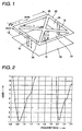
- a radiating electrode 22 having a planar outer shape of a square is disposed to be spaced apart from a grounding plate 10 and to be parallel to the grounding plate 10.
- the radiating electrode plate 22 is formed of a flat member, such as a conductive plate.
- Notched portions 24, each having an isosceles triangle shape, are provided in the radiating electrode 22.
- Each of the notched portions 24 has a lower side parallel to each side of the radiating electrode and has a vertex directed to the approximate center portion of the radiating electrode.
- the radiating electrode includes outer edge portions forming the square peripheries and a cross-shaped portion coupling four corners of the square.
- a feeding pin 14 is erected from the side of the grounding plate 10 and is electrically connected to the approximate center portion of the radiating electrode 22, that is, a crossing portion of the cross-shaped portion. Further, at the approximate intermediate locations of two opposing sides of the radiating electrode 22, a pair of short pins 16 is disposed to electrically connect the radiating electrode 22 and the grounding plate 10. The feeding pin 14 is electrically isolated from the grounding plate 10.
- a length of one side of the radiating electrode 22 is set to 84 mm and the height by which the one side of the radiating electrode 22 is spaced apart from the grounding plate 10 is set to 25 mm, so that a resonance frequency is 885 MHz, as shown in Fig. 2 .
- the notched portions 24 are provided and thus a resonance frequency is decreased.
- a radiating electric field is not generated in a zenith direction.
- the high resonance frequency of 2045 MHz is also obtained.
- the planar antenna resonates in a common mode of ⁇ /2 through a current path having a total length (a + b + 2c + d + e) including the length "a" of the feeding pin 14, the length "b" from the center portion of the radiating electrode 22, to which the feeding pin 14 is connected, to the square corner, the reciprocal length of the length "c” from the corner to the intermediate location of the side where the short pin 16 is not connected and the current is not generated, the length "d” from the corner to the intermediate location of the side where the short pin 16 is disposed, and the length e" of the short pin 16.
- the notched portions 24 are provided in the radiating electrode 22 so as to intercept the straight line coupling the arrangement location of the feeding pin 14 and the arrangement locations of the short pins 16.
- the current length is elongated, and that even though the height by which the radiating electrode 22 is spaced apart from the grounding plate 10 is not increased due to the lengthening of the current path and the planar shape of the radiating electrode 22 is not expanded, the low resonance frequency can be obtained.
- the current does not flow at the two opposing sides of the radiating electrode 22 where the short pins 16 are connected, and the current is not generated at the intermediate locations of the facing two sides of the radiating electrode 22 where the short pins 16 are not connected and locations close to the connecting location of the feeding pin 14 at the cross-shaped portion.
- the planar antenna resonates as a top-load-type antenna of 3 ⁇ /4 through a current path having a total length (a + b + c) including the length "a" of the feeding pin 14, the length "b” from the center portion of the radiating electrode 22, to which the feeding pin 14 is connected, to the corner, and the length "c" from the corner to the intermediate location of the side where the short pin 16 is not connected and the current is not generated.
- the horizontal directivity is non-directivity, and the radiating electric field not being generated in the zenith direction is the same as in the case of the resonance frequency of 885 MHz.
- the result was obtained in which the lower resonance frequency was increased by about 10 MHz, as compared with that of Fig. 1 .
- the result was obtained in which the lower resonance frequency was increased by about 10 MHz, as compared with the first comparative example. Accordingly, it was determined that the lowest resonance frequency is obtained at the intermediate locations of the sides as the arrangement locations of the short pins 16.
- the short pins 16 were respectively disposed at the intermediate locations of the four sides of the radiating electrode 22.
- the height by which the radiating electrode 22 was spaced apart from the grounding plate 10 was set to 25 mm as in Fig. 1
- the length of one side of the radiating electrode plate having the planar outer shape needed to be set to 124 mm, such that it was much larger than that in Fig. 1 .
- the two pairs of short pins 16 were provided and the planar antenna resonated in a common mode of ⁇ /2 through a current path having a total length (a + b + d + e) including the length "a" of the feeding pin 14, the length "b” from the center portion of the radiating electrode, to which the feeding pin 14 was connected, to the corner, and the length "d” from the corner to the intermediate location of the side where the short pin 16 was disposed, and the length "e” of the short pin 16.
- the resonance frequency of 885 MHz the size of the planar outer shape of the square needed to be increased although non-directivity is enhanced.
- a second planar antenna will be described with reference to Figs. 7 to 9 .
- Fig. 7 the same members as those shown in Fig. 1 are denoted by the same reference numerals, and the repetitive description will be omitted.
- a radiating electrode 32 having a planar outer shape to be circular and made of a conductive thin film or the like is provided on an insulating resin plate 36, and is disposed to be spaced apart from the grounding plate 10 and to be parallel to the grounding plate 10.
- the radiating electrode 32 four fan-shaped notched portions 34 are provided. Each of the notched portions has a vertex angle of 90 degrees at which a vertex is directed toward the center portion of the planar outer shape.
- the radiating electrode includes an edge portion having a circular outer shape, and a cross-shaped portion.
- the feeding pin 14 is electrically connected to the approximate center portion of the planar outer shape, that is, a crossing portion of the cross-shaped portion.
- each of a pair of short pins 16 is disposed to electrically connect the radiating electrode 32 and the grounding plate 10.
- the resonance frequency of 868 MHz is obtained.
- the horizontal directivity is non-directivity.
- the notched portions 34 are provided in the radiating electrode 32 so as to intercept the straight line coupling the arrangement location of the feeding pin 14 and the arrangement locations of the short pins 16. Therefore, an antenna having a smaller size than the conventional M-type antenna can be obtained.
- a third planar antenna will be described with reference to Figs. 10 to 12 .
- Fig. 10 the same members as those shown in Fig. 1 are denoted by the same reference numerals, and the repetitive description will be omitted.
- a radiating electrode 42 is formed by using a flat conductive member.
- the radiating electrode 42 is provided to be spaced apart from the grounding plate 10 and to be parallel to the grounding plate 10.
- the radiating electrode 42 has the planar outer shape formed such that vertexes of two isosceles triangles are opposite to each other and the two isosceles triangles are symmetrical, and the bottom sides of the two isosceles triangles are parallel to each other.
- the length of the bottom side of each triangle is set to 84 mm and the interval between the two parallel bottom sides is set to 84 mm.
- triangular notches 44 are provided in the isosceles triangles.
- This planar shape is obtained by cutting the two sides of the radiating electrode 22 according to the first embodiment where the short pins 16 of the radiating electrode 22 are not disposed.
- the height by which the radiating electrode 42 is spaced apart from the grounding plate 10 is set to 25 mm, as in Fig. 1 .
- the feeding pin 14 is erected from the side of the grounding plate 10 so as to be electrically connected to the center portion.
- the pair of short pins 16 are disposed so as to electrically connect the radiating electrode 42 and the grounding plate 10.
- the lower resonance frequency of 976 MHz and the higher resonance frequency of 2180 MHz are obtained.
- the horizontal directivity of the lower resonance frequency of 976 MHz is non-directivity, as shown in Fig. 12 .
- the planar antenna in the simulation of the current distribution in the operation at the resonance frequency of 976 MHz, it is determined that the planar antenna resonates in a common mode of ⁇ /2 through a current path having a total length (a + b + d + e) including the length "a" of the feeding pin 14, the length "b” from the center portion of the radiating electrode to the triangular corner, the length "d” from the corner to the intermediate location of the bottom side where the short pin 16 is disposed, and the length "e” of the short pin 16.
- each of the radiating electrodes 22 and 42 is formed of a flat conductive member, while, in the second planar antenna, the radiating electrode 32 is formed of a conductive thin film.
- the radiating electrode may be formed of a conductive line, such as a copper electrical wire or a copper rod.
- the radiating electrode may be formed without providing a conductive line that linearly couples the arrangement location of the feeding pin 14 and the arrangement locations of the short pins 16.
- a fourth planar antenna in which the radiating electrode is formed by using the conductive line will be described with reference to Fig. 13 .
- the same members as those shown in Fig. 1 are denoted by the same reference numerals, and the repetitive description will be omitted.
- a radiating electrode 52 is formed of a conductive line 54.
- the planar shape of the radiating electrode 52 is the same as that of the first planar antenna, but its width is very narrower than the width of the radiating electrode that is formed of the flat conductive member. Accordingly, the current path length is substantially increased, and even when the planar size is the same as that of the first planar antenna, its height may be set to the height smaller than 16.5 mm. In the fourth planar antenna, a narrower band is achieved, as compared with the first planar antenna.
- planar shape of the radiating electrodes can be varied shown in Figs. 14 to 27 .
- reference numeral 14 indicates a location where the feeding pin 14 is connected to a radiating electrode 62
- reference numeral 16 indicates a location where the short pin 16 is connected to the radiating electrode 62.
- Fig. 14 shows a fifth planar antenna.
- the cross-shaped portion couples the intermediate portions of the respective sides of a square frame portion
- the feeding pin 14 is electrically connected to the center portion of the cross-shaped portion
- a pair of short pins 16 are disposed at two diagonal corners of the square frame portion.
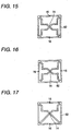
- Fig. 15 shows a first embodiment of the invention.
- the length of the radiating electrode is increased by bending each of the arms forming the cross-shaped portion shown in Fig. 1 .
- the short pins 16 may be disposed at sides different from those shown in Fig. 15 .
- Fig. 17 shows a second embodiment of the invention.
- the length of the radiating electrode is increased by bending some of the arms forming the cross-shaped portion and the others are not bent.
- the short pins 16 may be disposed at sides different from those shown in Fig. 17 .
- Fig. 19 shows a sixth planar antenna.
- the center part of a radiation electrode 62 is formed by a single linear portion and both ends of the linear portion are branched and coupled to the respective corners of a square frame portion.
- the short pins 16 may be disposed at sides different from those shown in Fig. 19 .
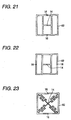
- Fig. 21 shows a seventh planar antenna.
- the center part of a radiation electrode 62 is formed by a single linear portion and both ends of the linear portion are branched and coupled to two sides of a square frame portions where the short pins 16 are provided, thereby forming an H-shaped portion.
- the short pins 16 may be disposed at sides different from those shown in Fig. 21 .
- Fig. 23 shows a third embodiment of the invention.
- each of the arms forming the cross-shaped portion shown in Fig. 1 is bent in a meandering manner, so that its length is increased.
- Fig. 24 shows an eigth planar antenna.
- the edge portions of the circular arc shape in the second embodiment shown in Fig. 7 where the short pins 16 are not disposed are removed, that is, the triangular bottom side in the third embodiment shown in Fig. 10 has an arcuate shape becoming convex:
- Fig. 25 shows a ninth planar antenna.
- the radiating electrode 62 has a shape in which two rings having the same shape are disposed such that portions of the rings come into contact with each other or overlap each other, the feeding pin 14 is disposed at a portion where two rings come into contact with each other, and the short pins 16 are respectively disposed at the other locations of the rings on a line passing through the arrangement location of the feeding pin 14.
- Fig. 26 shows a tenth planar antenna.
- the radiating electrode 62 has a shape in which two rectangular frames having the same shape are disposed such that portions of the rectangular frames come into contact with each other or overlap each other, the feeding pin 14 is disposed at a portion where two rectangular frames come into contact with each other, and the short pins 16 are respectively disposed at the other locations of the rectangular frames on a line passing through the arrangement location of the feeding pin 14.
- Fig. 27 shows an eleventh planar antenna.
- the radiation electrode 62 has a shape in which two triangular frames having the same shape are disposed such that portions of the triangular frames come in contact with each other or overlap each other, the feeding pin 14 is disposed at a portion where two triangular frames come in contact with each other, and the short pins 16 are respectively disposed at locations corresponding to uncommon apexes of the triangular frames.
- a twelfth planar antenna will be described with reference to Fig. 28 .
- the same members as those shown in Fig. 1 are denoted by the same reference numerals, and the repetitive description will be omitted.
- an additional antenna is provided in the notched portion of the radiating electrode or the portion where the conductive line of the radiating electrode is not provided, in the above-described embodiments.
- the shape of the radiating electrode 22 is the same as that of the first planar antenna.
- a GPS patch antenna 56 is disposed on a pedestal in one of the notched portions 24. With this configuration, the space can be effectively used, and the GPS patch antenna 56 is incorporated as an additional antenna. Therefore, the installation space and the height do not need to be increased even in a case where the plurality of antennas are disposed.
- the additional antenna may be provided at the other portion where the conductive line 54 of the radiating electrode 52 shown in Fig. 13 is not provided or at the portions where the notched portions 34, 44 shown in Figs. 7 and 10 are formed. Moreover, a further additional antenna may be provided in such positions as required.
- a thirteenth planar antenna will be described with reference to Figs. 29 to 31 .
- the same members as those shown in Fig. 1 are denoted by the same reference numerals, and the repetitive description will be omitted.
- a radiating electrode 66 formed by a conductive member such as a conductive thin film is provided on an insulative resin plate 64.
- the radiating electrode 66 includes outer edge portions forming the square peripheries and a cross-shaped portion coupling four corners of the square.
- a feeding pin 14 is electrically connected to an approximate center portion of the radiating electrode 66, that is, a crossing portion of the cross-shaped portion.
- a pair of short pins 16 is disposed.
- the insulative resin plate 64 is disposed in parallel to a grounding plate 10 in a state where the insulative resin plate is 64 is spaced apart from the grounding plate 10 at a predetermined height.
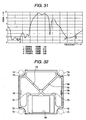
- a square hole 68 that is punched in the insulative resin plate 64 is provided to form a space for disposing another antenna.
- Gaps 70 are formed by cutting the conductive members of the cross-shaped portions between the center portions and the corners of the radiating electrode 66. It is preferable that the locations where the gaps 70 are provided may be approximately the locations where no current is generated in the resonance operation at the high resonance frequency.
- the gaps 70 do not affect the high resonance frequency, but affect the low resonance frequency. Specifically, since the locations where the gaps 70 are provided are not the locations where no current is generated in the resonance operation at the low resonance frequency, the capacitive coupling is established, so that the gaps 70 serve as loading capacitors, and the low resonance frequency is shifted so as to close to the high resonance frequency. As a result, the band of the high resonance frequency is widened and the gain is increased.
- Fig. 30 shows VSWR characteristics of the case where the gaps 70 are provided
- Fig. 31 shows VSWR characteristics of the case where the gaps 70 are not provided. That is, as shown in Fig. 31 , VSWR characteristics in the high resonance frequency bands of 1940 MHz and 2150 MHz in the case where the gaps 70 are not provided are 3.19 and 3.60, respectively.
- VSWR characteristics in the high resonance frequency bands of 1940 MHz and 2150 MHz in the case where the gaps 70 are provided are improved to 2.11 and 2.46, respectively, and the bands are widened.
- the respective gains are -5.25 dBi and -5.36 dBi.
- the respective gains are improved to -2.01 dBi and -2.22 dBi.
- the interval between the gaps 70 is increased, the coupling capacity is decreased, the wavelength reduction effect is increased. Therefore, it is preferable to appropriately set the interval in the gaps.
- Fig. 32 shows a fourth embodiment of the invention.
- arc-shaped notched portions 72 for screws are provided at four corners of the insulative resin plate 64.
- This embodiment has a structure that avoids mechanical interference with the screws 74 for fixing a radome covering the planar antenna. Therefore, the outer circumferential portion of the radiating electrode 66 is not necessarily square, and may be approximately square.
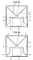
- Fig. 33 shows a fifth embodiment of the invention.
- the same members as those shown in Fig. 29 are denoted by the same reference numerals, and the repetitive description will be omitted.
- chip capacitors 76 are interposed in the gaps 70 that are provided in the cross-shaped portion of the radiating electrode 66 shown in Fig. 29 .
- a coupling capacity can be arbitrarily set, and the low resonance frequency can arbitrarily shifted so as to close to the high resonance frequency, which improves the characteristics of the high resonance frequency.
- Fig. 34 shows a sixth embodiment of the invention.
- the same members as those shown in Fig. 29 are denoted by the same reference numerals, and the repetitive description will be omitted.
- conductive members of the cross-shaped portions of the radiating electrode 66 are cut at the locations close to the corner portions so as to form the gaps, and chip inductors 78 are interposed in the gaps.
- the chip inductors 78 serve as extension coils, and thus it is possible to obtain an effect of decreasing the high resonance frequency. Accordingly, it is possible to obtain the same effect as that in the case where the meander elements are interposed at the locations where the chip inductors 78 are interposed.
- the chip inductors are preferably provided at the locations where the maximum current flows in the resonance operation at the high resonance frequency.
Landscapes
- Engineering & Computer Science (AREA)
- Computer Networks & Wireless Communication (AREA)
- Details Of Aerials (AREA)
- Variable-Direction Aerials And Aerial Arrays (AREA)
- Waveguide Aerials (AREA)
Claims (10)
- Antenne planaire, comprenant :un élément de plaque (10), adapté pour être électriquement mis à la terre ;une électrode de rayonnement (62, 66), à l'opposé de l'élément de plaque (10) avec un espace et s'étendant parallèlement à l'élément de plaque (10) ;une tige d'alimentation (14), disposée dans la partie centrale de l'électrode de rayonnement (62, 66), et adaptée pour alimenter l'électrode de rayonnement ;
etau moins une paire de tiges courtes (16), connectant électriquement l'élément de plaque (10) et un bord externe de l'électrode de rayonnement (62, 66) à des positions symétriques par rapport à la tige d'alimentation (14),dans laquelle l'électrode de rayonnement (62, 66) comprend des parties vides (24, 44) qui sont situées à des positions telles qu'elles sont sur les lignes droites hypothétiques connectant la tige d'alimentation (14) et les tiges courtes (16), caractérisée en ce que l'électrode de rayonnement (62, 66) est une plaque conductrice comprenant quatre parties vides (24, 44), dans laquelle l'électrode de rayonnement (62, 66) comprend des parties de bord externes formant un carré ou un carré approximatif et une partie en forme de croix avec une partie de croisement dans la partie centrale et avec quatre bras couplant les quatre coins du carré, et la longueur de l'électrode de rayonnement (62, 66) est accrue en courbant chacun ou certains des bras. - Antenne planaire selon la revendication 1, dans laquelle :une seule paire de tiges courtes (16) est prévue.
- Antenne planaire selon la revendication 1, dans laquelle :les tiges courtes (16) sont disposées sur des parties intermédiaires de deux côtés opposés de la plaque conductrice.
- Antenne planaire selon la revendication 1, comprenant en outre :une antenne supplémentaire (56) disposée sur l'élément de plaque (10) de sorte à s'opposer à l'une des parties vides (24).
- Antenne planaire selon la revendication 1, dans laquelle :des parties de l'électrode de rayonnement (66) définies entre les parties vides sont partiellement coupées pour former des espaces (70).
- Antenne planaire selon la revendication 5, comprenant en outre :des condensateurs pastilles (76), respectivement disposés dans les espaces (70).
- Antenne planaire selon la revendication 5, comprenant en outre :des inducteurs pastilles (78), respectivement disposés dans les espaces (70).
- Antenne planaire selon l'une quelconque des revendications précédentes, dans laquelle l'électrode de rayonnement (62, 66) est sous la forme d'un film mince conducteur disposé sur une plaque de résine isolante (64).
- Antenne planaire selon la revendication 8, dans laquelle un trou carré (68) est formé dans la plaque de résine isolante (64) pour former un espace en vue de disposer une antenne supplémentaire (56).
- Antenne planaire selon la revendication 8 ou 9, dans laquelle des parties encochées en forme d'arc (72) pour des vis sont prévues à chaque coin de la plaque de résine isolante (64).
Applications Claiming Priority (2)
| Application Number | Priority Date | Filing Date | Title |
|---|---|---|---|
| JP2006013684 | 2006-01-23 | ||
| JP2007010047A JP2007221774A (ja) | 2006-01-23 | 2007-01-19 | 平面型アンテナ |
Publications (2)
| Publication Number | Publication Date |
|---|---|
| EP1814193A1 EP1814193A1 (fr) | 2007-08-01 |
| EP1814193B1 true EP1814193B1 (fr) | 2009-03-18 |
Family
ID=37852326
Family Applications (1)
| Application Number | Title | Priority Date | Filing Date |
|---|---|---|---|
| EP07001318A Ceased EP1814193B1 (fr) | 2006-01-23 | 2007-01-22 | Antenne planaire |
Country Status (4)
| Country | Link |
|---|---|
| US (1) | US7518567B2 (fr) |
| EP (1) | EP1814193B1 (fr) |
| JP (1) | JP2007221774A (fr) |
| DE (1) | DE602007000692D1 (fr) |
Families Citing this family (25)
| Publication number | Priority date | Publication date | Assignee | Title |
|---|---|---|---|---|
| EP1801939B1 (fr) * | 2004-09-30 | 2013-03-06 | Japan Science and Technology Agency | Dispositif de rayonnement de lumiere infrarouge, dispositif de detection de lumiere infrarouge, spectrometre a impulsions de conversion de serie chronologique, et procede de rayonnement de lumiere infrarouge |
| JP4780662B2 (ja) * | 2006-06-15 | 2011-09-28 | 株式会社ヨコオ | 平面型アンテナ |
| USD606057S1 (en) * | 2009-01-30 | 2009-12-15 | Impinj. Inc. | Set of waveguide assisted antenna elements for RFID tags |
| WO2011032153A2 (fr) * | 2009-09-14 | 2011-03-17 | World Products Llc | Antennes conformées à un compteur optimisées |
| JP4875174B2 (ja) | 2010-02-12 | 2012-02-15 | 株式会社東芝 | カプラ装置 |
| JP5562080B2 (ja) * | 2010-03-17 | 2014-07-30 | 日本無線株式会社 | アンテナ |
| USD635963S1 (en) | 2010-09-10 | 2011-04-12 | World Products, Llc | Antenna |
| USD635964S1 (en) | 2010-09-14 | 2011-04-12 | World Products, Llc | Antenna |
| USD636382S1 (en) | 2010-09-14 | 2011-04-19 | World Products, Llc | Antenna |
| USD656925S1 (en) | 2011-07-21 | 2012-04-03 | World Products, Llc | Three-dimensional antenna |
| JP2013098791A (ja) * | 2011-11-01 | 2013-05-20 | Mitsubishi Cable Ind Ltd | アンテナ |
| CN102882004B (zh) * | 2012-06-29 | 2016-08-03 | 华为技术有限公司 | 一种电磁耦极子天线 |
| CN205429167U (zh) * | 2016-03-11 | 2016-08-03 | 中磊电子(苏州)有限公司 | 天线装置 |
| CN206673105U (zh) * | 2017-04-07 | 2017-11-24 | 深圳市景程信息科技有限公司 | 小型化斧形双模单极子天线 |
| JP7216577B2 (ja) | 2019-03-05 | 2023-02-01 | 日本航空電子工業株式会社 | アンテナ |
| JP7216576B2 (ja) | 2019-03-05 | 2023-02-01 | 日本航空電子工業株式会社 | アンテナ |
| WO2020240895A1 (fr) * | 2019-05-27 | 2020-12-03 | 株式会社村田製作所 | Étiquette rfid |
| JP6729843B1 (ja) * | 2019-05-27 | 2020-07-29 | 株式会社村田製作所 | Rfidタグ |
| WO2021000097A1 (fr) * | 2019-06-29 | 2021-01-07 | 瑞声声学科技(深圳)有限公司 | Antenne et dispositif électronique |
| JP7368134B2 (ja) * | 2019-07-26 | 2023-10-24 | 株式会社ヨコオ | アンテナ装置 |
| CN110289494B (zh) * | 2019-08-21 | 2019-11-26 | 南京邮电大学 | 一种三模零点频扫天线 |
| CN111106435A (zh) * | 2019-12-05 | 2020-05-05 | 瑞声精密制造科技(常州)有限公司 | 天线振子 |
| JP7437143B2 (ja) | 2019-12-05 | 2024-02-22 | 日本航空電子工業株式会社 | アンテナ |
| WO2021109089A1 (fr) * | 2019-12-05 | 2021-06-10 | 瑞声声学科技(深圳)有限公司 | Élément d'antenne |
| CN114122690B (zh) * | 2021-11-11 | 2023-09-19 | 京信通信技术(广州)有限公司 | 辐射单元、天线及基站 |
Family Cites Families (6)
| Publication number | Priority date | Publication date | Assignee | Title |
|---|---|---|---|---|
| JPH05136625A (ja) | 1991-01-11 | 1993-06-01 | Hiroyuki Arai | 平面型ダイバーシチアンテナ |
| EP1036434B1 (fr) * | 1997-12-05 | 2003-08-06 | Thomson Licensing S.A. | Appareil d'accord d'antenne vhf/uhf a commande automatique de gain |
| SE517218C2 (sv) | 1999-09-03 | 2002-05-07 | Ericsson Telefon Ab L M | En lågprofilantennstruktur samt en anordning innefattande trådlöst kommunikationsmedel, en trådlös mobil terminal, ett datorkort lämpligt för införande i en elektronisk anordning och ett lokalt nätverkssystem innefattande en basstation och ett flertal terminaler vilka är i trådlös kommunikation med basstationen innefattande en sådan lågprofilantennstruktur |
| FR2811479B1 (fr) * | 2000-07-10 | 2005-01-21 | Cit Alcatel | Antenne a couche conductrice et dispositif de transmission bi-bande incluant cette antenne |
| US6762729B2 (en) * | 2001-09-03 | 2004-07-13 | Houkou Electric Co., Ltd. | Slotted bow tie antenna with parasitic element, and slotted bow tie array antenna with parasitic element |
| ITVI20030270A1 (it) | 2003-12-31 | 2005-07-01 | Calearo Antenne Srl | Antenna multibanda a fessure |
-
2007
- 2007-01-19 JP JP2007010047A patent/JP2007221774A/ja active Pending
- 2007-01-22 EP EP07001318A patent/EP1814193B1/fr not_active Ceased
- 2007-01-22 US US11/655,891 patent/US7518567B2/en not_active Expired - Fee Related
- 2007-01-22 DE DE602007000692T patent/DE602007000692D1/de active Active
Also Published As
| Publication number | Publication date |
|---|---|
| DE602007000692D1 (de) | 2009-04-30 |
| EP1814193A1 (fr) | 2007-08-01 |
| JP2007221774A (ja) | 2007-08-30 |
| US7518567B2 (en) | 2009-04-14 |
| US20070171132A1 (en) | 2007-07-26 |
Similar Documents
| Publication | Publication Date | Title |
|---|---|---|
| US7518567B2 (en) | Planar antenna | |
| US7843389B2 (en) | Complementary wideband antenna | |
| US9472846B2 (en) | Multi-band planar inverted-F (PIFA) antennas and systems with improved isolation | |
| JP2004088218A (ja) | 平面アンテナ | |
| KR100616545B1 (ko) | 이중 커플링 급전을 이용한 다중밴드용 적층형 칩 안테나 | |
| KR20030064717A (ko) | 트리플 밴드 내장형 안테나 | |
| JP4021642B2 (ja) | アンテナ構造及び無線装置 | |
| EP2518826A1 (fr) | Antenne plane en F inverse | |
| US7466270B2 (en) | Planar antenna | |
| JP2005312062A (ja) | 小型アンテナ | |
| JP5057580B2 (ja) | アンテナ素子 | |
| JPWO2011010725A1 (ja) | ダイポールアンテナ | |
| EP3370305B1 (fr) | Dispositif d'antenne | |
| JP4782203B2 (ja) | 超小型内蔵型アンテナ | |
| JP6152016B2 (ja) | 多共振アンテナ | |
| JP2009124582A (ja) | アンテナ | |
| CN112993575B (zh) | 一种WiFi全向天线 | |
| KR101021478B1 (ko) | 멀티밴드 옴니 안테나 | |
| US7446726B2 (en) | Antenna | |
| JP5858844B2 (ja) | アンテナ装置 | |
| WO2010023832A1 (fr) | Dispositif d’antenne | |
| JP4758883B2 (ja) | アンテナ、携帯端末 | |
| KR101316153B1 (ko) | 안테나 | |
| JP2005094325A (ja) | 板状広帯域アンテナ | |
| JP2014075650A (ja) | 複合アンテナ |
Legal Events
| Date | Code | Title | Description |
|---|---|---|---|
| PUAI | Public reference made under article 153(3) epc to a published international application that has entered the european phase |
Free format text: ORIGINAL CODE: 0009012 |
|
| AK | Designated contracting states |
Kind code of ref document: A1 Designated state(s): AT BE BG CH CY CZ DE DK EE ES FI FR GB GR HU IE IS IT LI LT LU LV MC NL PL PT RO SE SI SK TR |
|
| AX | Request for extension of the european patent |
Extension state: AL BA HR MK RS |
|
| 17P | Request for examination filed |
Effective date: 20080201 |
|
| AKX | Designation fees paid |
Designated state(s): DE FR GB IT |
|
| 17Q | First examination report despatched |
Effective date: 20080403 |
|
| GRAP | Despatch of communication of intention to grant a patent |
Free format text: ORIGINAL CODE: EPIDOSNIGR1 |
|
| GRAS | Grant fee paid |
Free format text: ORIGINAL CODE: EPIDOSNIGR3 |
|
| GRAA | (expected) grant |
Free format text: ORIGINAL CODE: 0009210 |
|
| AK | Designated contracting states |
Kind code of ref document: B1 Designated state(s): DE FR GB IT |
|
| REG | Reference to a national code |
Ref country code: GB Ref legal event code: FG4D |
|
| REF | Corresponds to: |
Ref document number: 602007000692 Country of ref document: DE Date of ref document: 20090430 Kind code of ref document: P |
|
| PLBE | No opposition filed within time limit |
Free format text: ORIGINAL CODE: 0009261 |
|
| STAA | Information on the status of an ep patent application or granted ep patent |
Free format text: STATUS: NO OPPOSITION FILED WITHIN TIME LIMIT |
|
| 26N | No opposition filed |
Effective date: 20091221 |
|
| PG25 | Lapsed in a contracting state [announced via postgrant information from national office to epo] |
Ref country code: IT Free format text: LAPSE BECAUSE OF FAILURE TO SUBMIT A TRANSLATION OF THE DESCRIPTION OR TO PAY THE FEE WITHIN THE PRESCRIBED TIME-LIMIT Effective date: 20090318 |
|
| REG | Reference to a national code |
Ref country code: FR Ref legal event code: PLFP Year of fee payment: 10 |
|
| REG | Reference to a national code |
Ref country code: FR Ref legal event code: PLFP Year of fee payment: 11 |
|
| REG | Reference to a national code |
Ref country code: FR Ref legal event code: PLFP Year of fee payment: 12 |
|
| PGFP | Annual fee paid to national office [announced via postgrant information from national office to epo] |
Ref country code: FR Payment date: 20191216 Year of fee payment: 14 |
|
| PGFP | Annual fee paid to national office [announced via postgrant information from national office to epo] |
Ref country code: DE Payment date: 20200107 Year of fee payment: 14 Ref country code: GB Payment date: 20200115 Year of fee payment: 14 |
|
| REG | Reference to a national code |
Ref country code: DE Ref legal event code: R119 Ref document number: 602007000692 Country of ref document: DE |
|
| GBPC | Gb: european patent ceased through non-payment of renewal fee |
Effective date: 20210122 |
|
| PG25 | Lapsed in a contracting state [announced via postgrant information from national office to epo] |
Ref country code: FR Free format text: LAPSE BECAUSE OF NON-PAYMENT OF DUE FEES Effective date: 20210131 |
|
| PG25 | Lapsed in a contracting state [announced via postgrant information from national office to epo] |
Ref country code: GB Free format text: LAPSE BECAUSE OF NON-PAYMENT OF DUE FEES Effective date: 20210122 Ref country code: DE Free format text: LAPSE BECAUSE OF NON-PAYMENT OF DUE FEES Effective date: 20210803 |