EP1815607B1 - Kontaktkonfiguration zur verringerung von übersprechen in einem kommunikationssystem - Google Patents
Kontaktkonfiguration zur verringerung von übersprechen in einem kommunikationssystem Download PDFInfo
- Publication number
- EP1815607B1 EP1815607B1 EP05810854A EP05810854A EP1815607B1 EP 1815607 B1 EP1815607 B1 EP 1815607B1 EP 05810854 A EP05810854 A EP 05810854A EP 05810854 A EP05810854 A EP 05810854A EP 1815607 B1 EP1815607 B1 EP 1815607B1
- Authority
- EP
- European Patent Office
- Prior art keywords
- pair
- contact
- contacts
- signal
- conductors
- Prior art date
- Legal status (The legal status is an assumption and is not a legal conclusion. Google has not performed a legal analysis and makes no representation as to the accuracy of the status listed.)
- Expired - Lifetime
Links
Images



Classifications
-
- H—ELECTRICITY
- H04—ELECTRIC COMMUNICATION TECHNIQUE
- H04M—TELEPHONIC COMMUNICATION
- H04M3/00—Automatic or semi-automatic exchanges
- H04M3/18—Automatic or semi-automatic exchanges with means for reducing interference or noise; with means for reducing effects due to line faults with means for protecting lines
-
- H—ELECTRICITY
- H01—ELECTRIC ELEMENTS
- H01R—ELECTRICALLY-CONDUCTIVE CONNECTIONS; STRUCTURAL ASSOCIATIONS OF A PLURALITY OF MUTUALLY-INSULATED ELECTRICAL CONNECTING ELEMENTS; COUPLING DEVICES; CURRENT COLLECTORS
- H01R13/00—Details of coupling devices of the kinds covered by groups H01R12/70 or H01R24/00 - H01R33/00
- H01R13/646—Details of coupling devices of the kinds covered by groups H01R12/70 or H01R24/00 - H01R33/00 specially adapted for high-frequency, e.g. structures providing an impedance match or phase match
- H01R13/6461—Means for preventing cross-talk
-
- H—ELECTRICITY
- H01—ELECTRIC ELEMENTS
- H01R—ELECTRICALLY-CONDUCTIVE CONNECTIONS; STRUCTURAL ASSOCIATIONS OF A PLURALITY OF MUTUALLY-INSULATED ELECTRICAL CONNECTING ELEMENTS; COUPLING DEVICES; CURRENT COLLECTORS
- H01R13/00—Details of coupling devices of the kinds covered by groups H01R12/70 or H01R24/00 - H01R33/00
- H01R13/646—Details of coupling devices of the kinds covered by groups H01R12/70 or H01R24/00 - H01R33/00 specially adapted for high-frequency, e.g. structures providing an impedance match or phase match
- H01R13/6473—Impedance matching
-
- H—ELECTRICITY
- H01—ELECTRIC ELEMENTS
- H01R—ELECTRICALLY-CONDUCTIVE CONNECTIONS; STRUCTURAL ASSOCIATIONS OF A PLURALITY OF MUTUALLY-INSULATED ELECTRICAL CONNECTING ELEMENTS; COUPLING DEVICES; CURRENT COLLECTORS
- H01R13/00—Details of coupling devices of the kinds covered by groups H01R12/70 or H01R24/00 - H01R33/00
- H01R13/646—Details of coupling devices of the kinds covered by groups H01R12/70 or H01R24/00 - H01R33/00 specially adapted for high-frequency, e.g. structures providing an impedance match or phase match
- H01R13/6473—Impedance matching
- H01R13/6477—Impedance matching by variation of dielectric properties
-
- H—ELECTRICITY
- H01—ELECTRIC ELEMENTS
- H01R—ELECTRICALLY-CONDUCTIVE CONNECTIONS; STRUCTURAL ASSOCIATIONS OF A PLURALITY OF MUTUALLY-INSULATED ELECTRICAL CONNECTING ELEMENTS; COUPLING DEVICES; CURRENT COLLECTORS
- H01R4/00—Electrically-conductive connections between two or more conductive members in direct contact, i.e. touching one another; Means for effecting or maintaining such contact; Electrically-conductive connections having two or more spaced connecting locations for conductors and using contact members penetrating insulation
- H01R4/24—Connections using contact members penetrating or cutting insulation or cable strands
- H01R4/2416—Connections using contact members penetrating or cutting insulation or cable strands the contact members having insulation-cutting edges, e.g. of tuning fork type
-
- H—ELECTRICITY
- H01—ELECTRIC ELEMENTS
- H01R—ELECTRICALLY-CONDUCTIVE CONNECTIONS; STRUCTURAL ASSOCIATIONS OF A PLURALITY OF MUTUALLY-INSULATED ELECTRICAL CONNECTING ELEMENTS; COUPLING DEVICES; CURRENT COLLECTORS
- H01R4/00—Electrically-conductive connections between two or more conductive members in direct contact, i.e. touching one another; Means for effecting or maintaining such contact; Electrically-conductive connections having two or more spaced connecting locations for conductors and using contact members penetrating insulation
- H01R4/24—Connections using contact members penetrating or cutting insulation or cable strands
- H01R4/2416—Connections using contact members penetrating or cutting insulation or cable strands the contact members having insulation-cutting edges, e.g. of tuning fork type
- H01R4/242—Connections using contact members penetrating or cutting insulation or cable strands the contact members having insulation-cutting edges, e.g. of tuning fork type the contact members being plates having a single slot
Definitions
- the present invention relates to a crosstalk reducing contact configuration in a communication system.
- the present invention relates to positioning emitting a receiving conductive paths in a communication system in order to reduce NEXT, FEXT, Alien NEXT, Alien FEXT and increase Signal to Noise Ratio (SNR).
- SNR Signal to Noise Ratio
- Assemblies for transmitting telecommunications signals at high frequencies via twisted pairs of conductors currently use a variety of means, such as shielding and the like to ensure that the interference (such as Alien NEXT) between adjacent cables and connectors in a system is minimised.
- These prior art systems typically suffer from the drawback that the reduction in Alien NEXT between adjacent cables and connectors is insufficient for data transfers at and above 10 gigabits per second.
- existing designs for ports (or jacks) are sufficient to achieve only about a 55 ⁇ B SNR, which is insufficient to meet the proposed 70dB SNR necessary for the proposed 10gig development standard.
- Document US-A-2003/0095395 shows an assembly according to the preamble of claim 8.
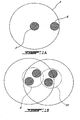
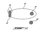
- Figures 1A through 1C provide transverse cross sectional views of conductors.
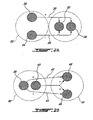
- Figures 2A and 2B provide transverse cross sections of emitting and receiving conductors.
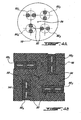
- Figures 3A through 3C provide transverse cross sections of conductor configurations.
- Figures 4A and 4B provide transverse cross sections of cable configurations.
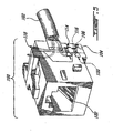
- Figure 5 provides a side perspective view of a connector jack and cable.
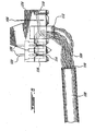
- Figure 6 provides a side plan view of a twisted pair cable connected to the connector jack rear panel of Figure 5 ;
- FIG. 7 schematically illustrates the general electromagnetic radiation pattern generated by a standard Insulation Displacement Connector (IDC) in the presence of an electric potential;
- IDC Insulation Displacement Connector
- FIGS 8A and 8B schematically illustrate connector configurations for reduced ANEXT and AFEXT in accordance with the present invention
- Figure 9 schematically illustrates alternative balanced pair configurations for reduced crosstalk.
- Figure 10 schematically illustrates alternative connector or port configurations for reduced crosstalk.
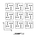
- Figure 11 schematically illustrates a possible periodic connector configuration for reduced ANEXT and AFEXT in accordance with an illustrative embodiment of the present invention.
- this coupling effect can be further exacerbated, in cases where an emitting conductor 12 comprises a substantially flat transverse cross section, as a parasitic signal 14 generated by signals propagating along the conductor 12 is emitted in a concentrated region generally perpendicular to the long surfaces 16 of the flat conductor 12.
- a second conductor 18 which finds itself located opposite one of the long surfaces 16 will be subjected to an increased parasitic signal 14.
- a third conductor 20 located outside of the main lobe of the parasitic signal 14 will be subject to a reduced electromagnetic field with a subsequent reduction in the coupling effect and noise induced by signals propagating along the flat conductor 12.
- balanced pairs of conductors 22 are used to propagate differential signals, with a first conductor 24 propagating a signal which is essentially the inverse of a signal propagated by a second conductor 26. These inverse signals give rise to first and second differential parasitic signals 28 and 30 being emitted by the conductors 24, 26. As a result, a third conductor 32 positioned in parallel and adjacent to the balanced pair 22 will receive the differential parasitic signals 28 and 30.
- the third conductor 32 By positioning the third conductor 32 such that the strengths (power) of the first parasitic signal 28 and the second parasitic signal 30 as received by the third conductor 32 are substantially the same, for example by placing the third conductor 32 such that the conductors 24, 26 are Symmetrical about the third conductor 32 (or in other words by placing the third conductor 32 such that it is equidistant to either of the conductors 24, 26), the amplitudes of the received first and second parasitic signals 28, 30 at any point in time will be opposite, giving rise to a cancelling effect in the third conductor 32. A similar effect will arise in a fourth conductor 34 (positioned in parallel and adjacent to the balanced pair 22) which is also positioned such that the strengths received first and second parasitic signals 28, 30 are substantially the same.
- first balanced pair 36 comprised of a first conductor 38 and a second conductor 40 give rise to first and second parasitic signals 42. 44 being emitted by the conductors 38, 40-
- third and fourth conductors 46, 48 which are arranged in parallel to the first and second conductors 38, 40 receive these parasitic signals 42, 44.
- the third and fourth conductors 46, 48 are of the same balanced pair 50, by positioning the third and fourth conductors 46, 48 such that the received strength of the first parasitic signal 42 is the same at both the third and fourth conductors 46, 48, and the received strength of the second parasitic signal 44 is the same at both the third and fourth conductors 46, 48, only common mode noise will be introduced onto the third and fourth conductors 46, 48. Given the balanced nature of the balanced pair 50, common mode noise is compensated for.
- the above generally described configurations can be taken advantage of in a number of implementations, some of which are described hereinbelow, in particular in the cases of transmission paths within cables and on PCBs and through connector interface assemblies.
- the above generally described configurations can be taken advantage either within a transmission path (for example in a transmission cable comprised of four balanced pairs of conductors), in order to reduce cross talk such as NEXT and FEXT, or between transmission paths (such as between adjacent connectors terminating different cables each comprised of four pairs of conductors), in order to reduce Alien cross talk such as ANEXT and AFEXT.
- a cable 52 (viewed in transverse cross section) comprises four (4) balanced pairs of conductors as in 54.
- the conductors as in 56 of adjacent balanced pairs as in 54 are oriented such that the noise induced by the conductor(s) of one balanced pair on the conductor(s) of an adjacent balanced pair is either differential and effectively cancelled, or common and thus is compensated for.
- this effect can be further enhanced by providing conductors as in 56 having an elongate transverse cross section, and ensuring that the conductors as in 56 of a first balanced pair are arranged such that they are not within the main lobe of the parasitic signals emitted by the conductor(s) of an adjacent balanced pair.
- the main lobe of the emitted parasitic signals is located generally in front of a long transverse surface as in 58, it generally suffices to ensure that the conductors of an adjacent balanced pair are not intersected by a line 60 which is perpendicular (or normal) to the long transverse surface(s) of a conductor of an adjacent balanced pair.
- a PCB 62 (viewed in transverse cross section) is shown.
- a similar effect can be applied in the case of the PCB 62 by arranging balanced pairs of conductors as in 64, each comprised of typically two (2) conductive traces as in 66 etched in the PCB 62, such that the noise induced by the conductor(s) of one balanced pair on the conductor(s) of an adjacent balanced pair is either differential and effectively cancelled, or common and compensated for.
- the conductive traces are typically flat (or rectangular)
- further improvements can be obtained by ensuring that the conductive traces as in 66 of an adjacent balanced pair are not intersected by a line 68 which is perpendicular (or normal) to the long transverse surface(s) as in 70 of a conductive trace 66 of an adjacent balanced pair.
- the PCB 62 as disclosed in Figure 3C is a multilayer PCB comprised of a first layer 72 bonded to a second layer 74, thereby allowing conductive traces as in 66 to be applied along a centre line 76 between the first and second layers 72. 74.
- the conductors as in 82 are oriented such that the noise induced by the conductors as in 82 of a first balanced pair 80 1 on the conductors as in 82 of an adjacent balanced pair 80 2 or 80 4 is either differential (as in the case of the conductors of balanced pair 80 4 ) and effectively cancelled, or common (as in the case of the conductors of balanced pair 80 2 ) and compensated for.
- a similar effect will be noted for other adjacent balanced pairs.
- the conductors as in 82 although all in parallel, may be stranded around the axis 84 such that they follow a helical (or winding) path along the length of the cable 78.
- a cable 86 (again viewed in transverse cross section) comprised of four balanced pairs 88 1 , 88 2 , 88 3 , 88 4 of conductors as in 90 is shown.
- the conductors as in 90 are positioned relative to one other about a central axis 92 of the cable 86 such that the noise induced by the conductors of a first balanced pair such as pair 88 1 on the conductors of adjacent balanced pairs 88 2 or 88 4 is either differential (as in the case of the conductors of balanced pair 88 4 ) and effectively cancelled, or common (as in the case of the conductors of balanced pair 88 2 ) and compensated for.
- the conductors as in 90 are of substantially rectangular (or elongate) transverse cross section, each having two long surfaces as in 94, with the long surfaces of the conductors as in 90 of a given balanced pair 88 1 , 88 2 , 88 3 or 88 4 lying in the same plane when viewed in transverse cross section.
- the conductors as in 90 of a given balanced pair are oriented such that their long surfaces as in 94 are substantially at right angles to the long surfaces as in 94 of conductors as in 90 of an adjacent balanced pair.
- each of the four balanced pairs 88 1 . 88 2 . 88 3 , 88 4 of conductors as in 90 is manufactured by encasing the conductors as in 90 within an insulation as in 96.
- the insulation as in 96 as illustrated is of substantially rectangular (or elongate) transverse cross section and is supported, in order to maintain the positioning of the balanced pairs, by a separator spline 98, typically manufactured from a pliable non-conductive insulating material such as plastic, having a substantially fylfot cross shaped transverse cross section.
- the conductors as in 90 all run in parallel, together with the spline 98 the conductors are typically stranded about the axis 92 such that they follow a helical, or winding, path along the length of the cable 86. Also, the assembly comprised of the spline 98 and the four balanced pairs 88 1 , 88 2 . 88 3 , 88 4 of conductors as in 90 would also typically be covered by a cable jacket (not shown).
- the connector assembly 100 generally refers to modular data transmission connectors having differential (balanced) transmission pairs (usually four (4) pairs).
- the connector 100 (or jack) provides an interface between two cables; a first cable (not shown) is usually terminated by a plug (also not shown), while a second cable, hereinafter referred to as connector cable 102, connects to the back panel 104 of connector 100, typically through a series of Insulation Displacement Connectors (IDCs) 106, or other connection means of the like.
- IDCs Insulation Displacement Connectors
- the connector cable 102 comprises four (4) twisted pairs of conductors 108 contained within an insulating cable jacket 110. As the pairs emerge from jacket 110, they are separated and guided through wire pair guide 112 to respective individual wire connector ports 114, both of which are part of the connector rear panel 104. ideally, the twisted pairs 108 remain tightly twisted all the way through the wire pair guide 112 in order to minimize induced parasitic capacitances between single wires.
- the wire pair guide 112, as well as connector port 114 are typically manufactured from an insulating material which provides adequate insulation and shielding between the pairs as they emerge from cable jacket 110, and subsequently between individual conductors of the pairs 108 when they are terminally inserted into the individual connector ports 114.
- an appropriate set of IDCs 106 or other similar connection means generally comprising a bifurcated end 116 for electrically connecting with individual contact wires 118, and an elongated end 120 for electrically connecting with appropriate jack circuit means, briefly described hereinbelow, reach through the connector ports 114 to make contact with the individual wires 118 of connector cable 102.
- the signals, transmitted through the IDCs 106 from the individual wires 118, are subsequently brought to a respective one of a plurality of connector blades as in 122 of the jack (for example, an RJ-45 jack) by appropriate jack circuit means for connection with, and transmission to, an appropriate cable plug (not shown).
- Such a jack circuit means may include a variety of electrical components, such as wires, printed circuit boards (PCB), flexible printed circuit boards (Flex PCB), or any combination thereof.
- the IDCs connect directly to a Flex PCB (not shown) through the elongated IDC ends 120 and a connecting material such as conductive solder (also not shown)
- the Flex PCB brings the transmitted signals directly to the connector blades 122 through a circuit printed thereof, which may be designed, if needed, to include various compensation capacitors that counterbalance parasitic reactances induced between the parallel connector blades 122.
- the IDCs 106 generally induce a certain amount of crosstalk between each other, either within a same connector (NEXT: Near End Crosstalk, FEXT: Far End Crosstalk), or between two adjacent connectors closely positioned together (AFEXT: Alien FEXT, ANEXT: Alien NEXT), which can significantly reduce the quality of the signals transmitted through the connector.
- NEXT Near End Crosstalk
- AFEXT Alien FEXT
- ANEXT Alien NEXT
- ANEXT Alien NEXT
- an IDC is made from a small metal conducting plate, figuratively illustrated in Figure 7 as a substantially flat rectangle when viewed in transverse cross section, which can act as an emitting antenna in the presence of an electric potential.
- a neighbouring, or adjacent IDC may act as a receiving antenna, and thus be affected (or coupled) by the parasitic signal provided by the emitting IDC.
- the parasitic signal emitted by the disturbing or emitting IDC pair 124 will emit a signal 126 which will be radiated outward in a direction primarily at right angles to a long surface 128, much like a typical antenna, generally following the illustrated radiation pattern 126.
- the disturbed or receiving IDC pair 130 will thus be affected by the radiated signal 126, and thus be a victim to crosstalk.
- a first disturbed IDC 132 is located closer to the emitting IDC pair 124 than a second disturbed IDC 134, and as a result the coupling effect will be greater for the first disturbed IDC 132 than the second disturbed IDC 134.
- the first disturbed IDC 132 will act as a partial shield to the second disturbed IDC 134. Consequently, the parasitic signal induced by the emitting IDC pair 124 on the former will be stronger than the one induced on the latter, generating significant, and generally undesirable, differential mode noise on the receiving pair 130.
- FIGS. 8A and 8B two novel connector configurations generally represented by respective numerals 136 and 138 will now be described.
- the configurations 136 and 138 present important improvements over the parallel configuration illustrated in Figure 7 . Namely, the contacts of adjacent pairs (first or nearest neighbour pairs in both in X and Y) are perpendicularly oriented such that the adjacent pair does not lie directly within the main lobes of the signals emitted by the other pair, and vice-versa. This is applicable to both adjacent pairs within the same connector as well as adjacent pairs in adjacent connectors.
- the residual irradiated signal affecting adjacent pairs will either be symmetrically irradiated to both contacts of such pairs, at worst generating common mode noise of minimal importance, or will be irradiated such that the parasitic signal from one contact will be self-balanced by the parasitic signal of the second contact, thus generating no significant resultant noise.
- first contact pair 140 and second contact pair 142 of a first connector 144 and first contact pair 146 and second contact pair 148 of a second connector 150 can be examined more closely.
- the first pair configuration (a) is that as utilised in the connector configuration 136 of Figure 8A .
- the other pair configurations provide a series of examples for reducing crosstalk between pairs, while not necessarily abiding by all of the aforementioned configuration guidelines. For example, (g) and (h) reduce crosstalk between pairs by their perpendicularity alone, whereas (a) and (e) provide reduced crosstalk based on both their mutual perpendicularity and irradiation symmetry.
- configuratons (a) through (f) presented in Figure 10 may be utilised to reduce alien crosstalk between adjacent connectors.
- Configurations (a), (b) and (f) of figure 10 used in the panel configuration of figure 11 are illustrative embodiments of the present invention.
- Configurations (c), (d) and (e) of figure 10 used in the panel configuration of figure 11 are not embodiments of the present invention.
- the panel configuration of Figure 11 illustrates a two-dimensionally periodic configuration (in X and Y) of contact pairs that both reduces pair-to-pair crosstalk within a same connector, but also between connectors through perpendicularity and symmetry of parasitic signal emission between adjacent balanced pairs both within and between connectors.
Landscapes
- Engineering & Computer Science (AREA)
- Signal Processing (AREA)
- Details Of Connecting Devices For Male And Female Coupling (AREA)
- Communication Cables (AREA)
- Coupling Device And Connection With Printed Circuit (AREA)
- Manufacturing Of Electrical Connectors (AREA)
- Connections By Means Of Piercing Elements, Nuts, Or Screws (AREA)
Claims (20)
- Verfahren zum Verringern von Übersprechen zwischen ersten und zweiten Kabeln in einem Datenübertragurigssystem, wobei jedes der Kabel aus einem Paar von Leitern besteht und das Verfahren folgende Schritte umfasst:Bereitstellen eines ersten im wesentlichen flachen Kontaktes (156), der mit einem ersten Leiter der beiden Leiter verbunden ist, wobei der erste Kontakt ein erstes Signal emittiert;Bereitstellen eines Paares (140) im wesentliche flacher Kontakte (152, 154), wobei jeder Kontakt des Kontaktpaares mit einem anderen Leiter des Leiterpaares des zweiten Kabels verbunden ist und ein Kontakt des Kontaktpaares ein zweites Signal emittiert, das im wesentlichen eine Umkehrung eines dritten Signals ist, das von einem anderen Kontakt des Kontaktpaares emittiert wird;Positionieren des ersten Kontaktes im Bezug auf das Kontaktpaar derart, dass eine Amplitude des ersten Signals, das an einem Kontakt des Kontaktpaares empfangen wird, im wesentlichen dieselbe ist wie die Amplitude des ersten Signals, das von einem anderen Kontakt des Kontaktpaares empfangen wird; undPositionieren des Kontaktpaares im Bezug auf den ersten Kontakt derart, dass eine Amplitude des zweiten Signals, das von dem ersten Kontakt empfangen wird, einer Amplitude des dritten Signals, das von dem ersten Kontakt empfangen wird, im wesentlichen gegenläufig ist;wobei eine lange Oberfläche des ersten Kontaktes senkrecht zu einer langen Oberfläche jedes Kontaktes des Kontaktpaares ausgerichtet ist.
- Verfahren nach Anspruch 1, weiterhin umfassend die Schritte des Bereitstellen eines zweiten Kontaktes, der mit einem zweiten Leiter des Leiterpaares des ersten Kabels verbunden ist, wobei der zweite Kontakt ein zweites Signal emittiert, und Positionieren des zweiten Kontaktes relativ zu dem Kontaktpaar derart, dass eine Amplitude des zweiten Signals, dass an einem Kontakt des zweiten Kontaktpaares empfangen wird, im wesentlichen dieselbe ist wie eine Amplitude des zweiten Signals, das an einem anderen Kontakt des zweiten Kontaktpaares empfangen wird.
- Verfahren nach Anspruch 1, bei dem der Positionierungsschritt das Plazierten des Kontaktpaares symmetrisch um den ersten Kontakt umfasst.
- Verfahren nach Anspruch 1, bei dem der Positionierungsschritt das Plazieren des ersten Kontaktes in gleichem Abstand von jedem Kontakt des Kontaktpaares umfasst.
- Verfahren nach Anspruch 1, bei dem der Positienierungsschritt das Plazieren des ersten Kontaktes derart umfasst, dass eine Linie, die senkrecht zu der langen Oberfläche eines Kontaktes des Kontaktpaares verläuft, den ersten Kontakt nicht schneidet.
- Verfahren nach Anspruch 1, bei dem beide Leiter des Leiterpaares verdrillt sind.
- Verfahren nach Anspruch 1, bei dem beide Leiter des Leiterpaares parallel sind.
- Anordnung zum Anschließen erster und zweiter Kabel in einem Telekommunikationssystem, wobei jedes der Kabel erste und zweite Leiter enthält, dadurch gekennzeichnet, dass die Anordnung enthält:einen ersten, im wesentlichen flachen Kontakt (156), der mit dem ersten Leiter des ersten Kabels verbunden ist, wobei der erste Kontakt ein erstes Signal emittiert, wenn er in Verwendung ist;einen im wesentlichen flachen zweiten Kontakt (158), der mit dem zweiten Leiter des ersten Kabels verbunden ist, wobei der zweite Kontakt ein zweites Signal emittiert; undein Paar (140) im wesentlichen flacher Kontakte, die mit einem jeweiligen Leiter der ersten und zweiten Leiter des zweiten Kabels verbunden sind, wobei ein Kontakt (152) des Kontaktpaars in Verwendung ein drittes Signal emittiert, das im wesentlichen eine Umkehrung eines vierten Signals ist, das in Verwendung von dem anderen Kontakt (154) des Kontaktpaares emittiert wird;wobei der erste Kontakt im Bezug auf das Kontaktpaar derart angeordnet ist, dass eine Amplitude des ersten Signals, das, wenn es emittiert wird, an einem Kontakt des Kontaktpaars empfangen wird, im wesentlichen dieselbe ist wie eine Amplitude des ersten Signals, das an dem anderen Kontakt des Kontaktpaares empfangen wird, und der zweite Kontakt im Bezug auf das Kontaktpaar derart angeordnet ist, dass eine Amplitude des zweiten Signals, das, wenn es emittiert wird, an dem einen Kontakt des Kontaktpaares empfangen wird, im wesentlichen dieselbe ist wie eine Amplitude des zweiten Signals, das von dem anderen Kontakt des Kontaktpaares empfangen wird,wobei des Kontaktpaar (140) im Bezug auf den ersten Kontakt (156) derart angeordnet ist, dass eine Amplitude des dritten Signals, das, wenn es emittiert wird, von dem ersten Kontakt empfangen wird, einer Amplitude des vierten Signals, das, wenn es emittiert wird, von dem ersten Kontakt empfangen wird, im wesentlichen gegenläufig ist und das Kontaktpaar im Bezug auf den zweiten Kontakt derart angeordnet ist, dass eine Amplitude des dritten Signals, das, wenn es emittiert wird, von dem zweiten Kontakt empfangen wird, einer Amplitude des vierten Signals, das, wenn es emittiert wird, von dem zweiten Kontakt empfangen wird, im wesentlichen gegenläufig ist,und weiterhin eine lange Oberfläche des ersten Kontaktes (156) parallel zu einer langen Oberfläche des zweiten Kontaktes (158) ist und die lange Oberfläche des ersten Kontaktes sowie die lange Oberfläche des zweiten Kontaktes in einem rechten Winkel zu einer langen Oberfläche eines der beiden Kontakte des Kontaktpaares (140) verlaufen.
- Anordnung nach Anspruch 8, bei der die lange Oberfläche des ersten Kontaktes gegenüberliegend zu der langen Oberfläche des zweiten Kontaktes angeordnet ist
- Anordnung nach Anspruch 8, bei der die Kontakte auf einer ersten Oberfläche der Anordnung angeordnet sind und weiterhin eine Vielzahl von Buchsen enthalten, die dazu eingerichtet sind, einen Kabelstecker aufzunehmen, der in einer zweiten Oberfläche derselben ausgeformt ist, wobei eine erste und eine zweite Buchse der Buchsen eine Vielzahl von Verkünderplättchen enthalten, die in diesen angeordnet sind, und ein Paar der Plättchen in der ersten Buchse mit jeweils einem des ersten Kontaktes und des zweiten Kontaktes verbunden ist und ein Paar der Plättchen in der zweiten Buchse mit einem entsprechenden Kontakt des Kontaktpaares verbunden ist.
- Anordnung nach Anspruch 8, weiterhin enthaltend eine Patchtafel, wobei die ersten und zweiten Kontakte auf einer ersten Oberfläche eines ersten modularen Verbinders angeordnet sind und das Kontaktpaar auf einer ersten Oberfläche eines zweiten modularen Verbinders angeordnet ist, wobei die Verbinder dazu eingerichtet sind, in die Patchtafel eingesteckt zu werden.
- Anordnung nach Anspruch 11, bei der die Verbinder nebeneinander auf der Patchtafel angeordnet sind.
- Anordnung nach Anspruch 11, bei der die Verbinder übereinander auf der Patchtafel angeordnet sind.
- Anordnung nach Anspruch 11, bei der jeder der Verbinder weiterhin eine Buchsen enthält, die dazu eingerichtet ist, einen Kabelstecker aufzunehmen, der auf einer zweiten Oberfläche derselben ausgeformt ist, wobei jeder der Buchsen eine Vielzahl von Verbinderplättchen aufweist, die in ihr angeordnet sind und eines der Plättchen in der Buchse des ersten Verbinders mit dem ersten Kontakt verbunden ist und ein Plättchenpaar in der Buchse des zweiten Verbinders mit einem entsprechenden Kontakt des zweiten Kontaktpaares verbunden ist.
- Anordnung nach Anspruch 11 oder 14, bei der die ersten und zweiten modularen Verbinder modulare Buchsen sind.
- Anordnung nach Anspruch 10, bei der jedes der Kabel vier verdrillte Paare von Leitern hat und jede der Buchsen acht Plättchen aufweist, die in dieser angeordnet sind.
- Anordnung nach Anspruch 10 oder 14, bei der jede der Buchsen dazu eingerichtet ist, einen RJ-45-Verbinderstecker aufzunehmen.
- Anordnung nach Anspruch 8, bei der das Kontaktpaar symmetrisch um den ersten Kontakt und den zweiten Kontakt angeordnet sind.
- Anordnung nach Anspruch 8, bei der die beiden flachen Kontakte in derselben Ebene liegen.
- Anordnung nach Anspruch 8, bei der die flachen Kontakte IDCs sind.
Priority Applications (1)
| Application Number | Priority Date | Filing Date | Title |
|---|---|---|---|
| EP11180114A EP2395676B1 (de) | 2004-11-17 | 2005-11-17 | Verbinder zur Nebensprechreduzierung und Kontaktkonfigurierung in einem Kommunikationssystem |
Applications Claiming Priority (3)
| Application Number | Priority Date | Filing Date | Title |
|---|---|---|---|
| US62813604P | 2004-11-17 | 2004-11-17 | |
| CA002487760A CA2487760A1 (en) | 2004-11-17 | 2004-11-17 | Connector and contact configuration therefore |
| PCT/CA2005/001753 WO2006053436A1 (en) | 2004-11-17 | 2005-11-17 | Crosstalk reducing conductor and contact configuration in a communication system |
Publications (3)
| Publication Number | Publication Date |
|---|---|
| EP1815607A1 EP1815607A1 (de) | 2007-08-08 |
| EP1815607A4 EP1815607A4 (de) | 2007-11-28 |
| EP1815607B1 true EP1815607B1 (de) | 2011-09-07 |
Family
ID=36406133
Family Applications (2)
| Application Number | Title | Priority Date | Filing Date |
|---|---|---|---|
| EP11180114A Expired - Lifetime EP2395676B1 (de) | 2004-11-17 | 2005-11-17 | Verbinder zur Nebensprechreduzierung und Kontaktkonfigurierung in einem Kommunikationssystem |
| EP05810854A Expired - Lifetime EP1815607B1 (de) | 2004-11-17 | 2005-11-17 | Kontaktkonfiguration zur verringerung von übersprechen in einem kommunikationssystem |
Family Applications Before (1)
| Application Number | Title | Priority Date | Filing Date |
|---|---|---|---|
| EP11180114A Expired - Lifetime EP2395676B1 (de) | 2004-11-17 | 2005-11-17 | Verbinder zur Nebensprechreduzierung und Kontaktkonfigurierung in einem Kommunikationssystem |
Country Status (9)
| Country | Link |
|---|---|
| US (2) | US8477928B2 (de) |
| EP (2) | EP2395676B1 (de) |
| JP (1) | JP2008521180A (de) |
| CN (1) | CN101099301A (de) |
| AT (1) | ATE523970T1 (de) |
| AU (1) | AU2005306539A1 (de) |
| CA (2) | CA2487760A1 (de) |
| MX (1) | MX2007005907A (de) |
| WO (1) | WO2006053436A1 (de) |
Families Citing this family (14)
| Publication number | Priority date | Publication date | Assignee | Title |
|---|---|---|---|---|
| DE202006013075U1 (de) * | 2006-08-25 | 2006-11-02 | CCS Technology, Inc., Wilmington | Anschlusssystem |
| DE102007002769B4 (de) * | 2007-01-18 | 2008-10-16 | Adc Gmbh | Anschlussklemmleiste |
| US8251737B2 (en) * | 2008-12-19 | 2012-08-28 | Fci | Terminal block for a cable connector |
| US7736159B1 (en) * | 2009-04-07 | 2010-06-15 | Tyco Electronics Corporation | Pluggable connector with differential pairs |
| US8262407B2 (en) * | 2009-12-01 | 2012-09-11 | Cisco Technology, Inc. | Active copper cable extender |
| US20120252088A1 (en) * | 2011-03-29 | 2012-10-04 | Jie Zhang | Floating magnet probe for cell isolation |
| US8900015B2 (en) | 2011-10-03 | 2014-12-02 | Panduit Corp. | Communication connector with reduced crosstalk |
| US20140027155A1 (en) * | 2012-07-25 | 2014-01-30 | Ametek, Inc. | Differential mode signal connector and cable assembly |
| JP2014138015A (ja) | 2013-01-15 | 2014-07-28 | Fujitsu Ltd | プリント基板及びプリント基板の製造方法 |
| EP3084890A4 (de) | 2013-12-20 | 2017-07-05 | PPC Broadband, Inc. | Hochfrequenzabschirmung für mikrokoaxialkabelverbinder |
| US20150318082A1 (en) * | 2014-04-30 | 2015-11-05 | Dell Products L.P. | Signal and Drain Arrangement for High Speed Cables |
| US10310126B2 (en) * | 2014-12-01 | 2019-06-04 | Subvision Ab | System and method for sea bed surveying |
| JP6281481B2 (ja) * | 2014-12-17 | 2018-02-21 | 株式会社オートネットワーク技術研究所 | コネクタ及び電線ユニット |
| JP7601739B2 (ja) * | 2021-10-08 | 2024-12-17 | ヒロセ電機株式会社 | 4個の端子を有するコネクタ部材を備えたコネクタ |
Family Cites Families (53)
| Publication number | Priority date | Publication date | Assignee | Title |
|---|---|---|---|---|
| US4295703A (en) * | 1978-11-27 | 1981-10-20 | Northern Telecom Limited | Connector block |
| CA1176330A (en) | 1983-11-08 | 1984-10-16 | Northern Telecom Limited | Double tap connector with insulation displacing terminals |
| FR2600825B1 (fr) | 1986-06-25 | 1988-08-26 | Mars Actel | Contact hermaphrodite pour conducteur electrique isole et connecteur comportant de tels contacts |
| US5186647A (en) * | 1992-02-24 | 1993-02-16 | At&T Bell Laboratories | High frequency electrical connector |
| JPH0785909A (ja) * | 1993-09-17 | 1995-03-31 | Kel Corp | 圧接コネクタ |
| US5599206A (en) * | 1995-08-04 | 1997-02-04 | The Whitaker Corporation | Modular jack subassembly for use in a network outlet |
| US6270372B1 (en) * | 1996-09-26 | 2001-08-07 | Panduit Corp. | Patch cord connector |
| US6074503A (en) * | 1997-04-22 | 2000-06-13 | Cable Design Technologies, Inc. | Making enhanced data cable with cross-twist cabled core profile |
| US5997358A (en) | 1997-09-02 | 1999-12-07 | Lucent Technologies Inc. | Electrical connector having time-delayed signal compensation |
| US5967853A (en) * | 1997-06-24 | 1999-10-19 | Lucent Technologies Inc. | Crosstalk compensation for electrical connectors |
| DK0995238T3 (da) * | 1997-07-10 | 2003-07-21 | Lk As | Konnektor til reduktion af signalkobling samt kabel omfattende en sådan konnektor |
| US5989071A (en) | 1997-09-03 | 1999-11-23 | Lucent Technologies Inc. | Low crosstalk assembly structure for use in a communication plug |
| US6238231B1 (en) * | 1997-09-03 | 2001-05-29 | Avaya Technology Corp. | Strain relief apparatus for use in a communication plug |
| JPH11185886A (ja) * | 1997-12-22 | 1999-07-09 | Matsushita Electric Works Ltd | 電気コネクタ |
| DE69902491T2 (de) * | 1998-02-27 | 2003-04-10 | Lucent Technologies Inc., Murray Hill | Steckverbinder mit geringem Übersprechen |
| US6126476A (en) * | 1998-03-23 | 2000-10-03 | The Siemon Company | Enhanced performance connector |
| US6150612A (en) * | 1998-04-17 | 2000-11-21 | Prestolite Wire Corporation | High performance data cable |
| DE19823647C1 (de) * | 1998-05-27 | 1999-09-23 | Metz Albert Ria Electronic | Mehrpolige Anschlußklemme für elektrische Leiter |
| AUPP484998A0 (en) * | 1998-07-24 | 1998-08-20 | Krone Aktiengesellschaft | Electrical connector |
| GB2343558B (en) | 1998-11-04 | 2002-10-30 | Itt Mfg Enterprises Inc | Electrical connector |
| US6309240B1 (en) * | 1998-12-21 | 2001-10-30 | Avaya Technology Corp. | Terminal strip for maintaining tip/ring orientation standards |
| US6193526B1 (en) * | 1999-02-16 | 2001-02-27 | Hubbell Incorporated | Wiring unit with angled insulation displacement contacts |
| GB9908097D0 (en) | 1999-04-09 | 1999-06-02 | Drewnicki Richard | Electrical connector |
| US6283768B1 (en) * | 1999-05-13 | 2001-09-04 | Ideal Industries, Inc. | RJ-45 style modular connector |
| US6582247B2 (en) * | 1999-09-30 | 2003-06-24 | The Siemon Company | Connecting block with staggered IDCs |
| US6270381B1 (en) * | 2000-07-07 | 2001-08-07 | Avaya Technology Corp. | Crosstalk compensation for electrical connectors |
| DE10051097C2 (de) | 2000-08-17 | 2002-11-28 | Krone Gmbh | Elektrischer Steckverbinder |
| US6592395B2 (en) * | 2001-10-03 | 2003-07-15 | Avaya Technology Corp. | In-line cable connector assembly |
| US6608764B2 (en) * | 2001-11-16 | 2003-08-19 | Adc Telecommunications, Inc. | Telecommunications patch panel |
| US6641411B1 (en) * | 2002-07-24 | 2003-11-04 | Maxxan Systems, Inc. | Low cost high speed connector |
| US6648670B1 (en) * | 2002-08-01 | 2003-11-18 | Surtec Industries Inc. | Dual-head IDC terminal |
| US6794570B2 (en) * | 2002-08-27 | 2004-09-21 | Hon Hai Precision Ind. Co., Ltd. | Bundle twisted-pair cable |
| US6881090B1 (en) | 2003-11-07 | 2005-04-19 | R & B Inc. | Rotatable no strip no crimp electrical connector for wires |
| CN1902785A (zh) | 2003-11-21 | 2007-01-24 | 莱维顿制造有限公司 | 串扰减少的插线面板系统和方法 |
| US7038918B2 (en) | 2004-03-03 | 2006-05-02 | Hubbell Incorporated | Midspan patch panel with compensation circuit for data terminal equipment, power insertion and data collection |
| CN2694487Y (zh) * | 2004-03-17 | 2005-04-20 | 鸿富锦精密工业(深圳)有限公司 | 散热器扣合装置 |
| US7179115B2 (en) * | 2004-04-26 | 2007-02-20 | Commscope Solutions Properties, Llc | Alien next compensation for adjacently placed connectors |
| US7190594B2 (en) | 2004-05-14 | 2007-03-13 | Commscope Solutions Properties, Llc | Next high frequency improvement by using frequency dependent effective capacitance |
| US7038554B2 (en) | 2004-05-17 | 2006-05-02 | Leviton Manufacturing Co., Inc. | Crosstalk compensation with balancing capacitance system and method |
| US7422467B2 (en) * | 2004-11-17 | 2008-09-09 | Belden Cdt (Canada), Inc. | Balanced interconnector |
| US7264516B2 (en) * | 2004-12-06 | 2007-09-04 | Commscope, Inc. | Communications jack with printed wiring board having paired coupling conductors |
| US7186149B2 (en) * | 2004-12-06 | 2007-03-06 | Commscope Solutions Properties, Llc | Communications connector for imparting enhanced crosstalk compensation between conductors |
| US7168993B2 (en) * | 2004-12-06 | 2007-01-30 | Commscope Solutions Properties Llc | Communications connector with floating wiring board for imparting crosstalk compensation between conductors |
| US7326089B2 (en) * | 2004-12-07 | 2008-02-05 | Commscope, Inc. Of North Carolina | Communications jack with printed wiring board having self-coupling conductors |
| US7186148B2 (en) | 2004-12-07 | 2007-03-06 | Commscope Solutions Properties, Llc | Communications connector for imparting crosstalk compensation between conductors |
| US7166000B2 (en) * | 2004-12-07 | 2007-01-23 | Commscope Solutions Properties, Llc | Communications connector with leadframe contact wires that compensate differential to common mode crosstalk |
| US7204722B2 (en) * | 2004-12-07 | 2007-04-17 | Commscope Solutions Properties, Llc | Communications jack with compensation for differential to differential and differential to common mode crosstalk |
| US7320624B2 (en) * | 2004-12-16 | 2008-01-22 | Commscope, Inc. Of North Carolina | Communications jacks with compensation for differential to differential and differential to common mode crosstalk |
| US7175476B2 (en) | 2005-01-11 | 2007-02-13 | Daeun Electronics Co., Ltd. | Crosstalk canceling pattern for high-speed communications and modular jack having the same |
| EP1842296A1 (de) * | 2005-01-28 | 2007-10-10 | Commscope Inc. of North Carolina | Gesteuerter moduswandlungsverbinder zur verminderung von fremdübersprechungen |
| US7314393B2 (en) * | 2005-05-27 | 2008-01-01 | Commscope, Inc. Of North Carolina | Communications connectors with floating wiring board for imparting crosstalk compensation between conductors |
| US7223115B2 (en) | 2005-06-03 | 2007-05-29 | Commscope, Inc. Of North Carolina | Cross-connect systems with connector blocks having balanced insulation displacement contacts |
| US7503798B2 (en) * | 2005-06-03 | 2009-03-17 | Commscope, Inc. Of North Carolina | Cross connect systems with self-compensating balanced connector elements |
-
2004
- 2004-11-17 CA CA002487760A patent/CA2487760A1/en not_active Abandoned
-
2005
- 2005-11-17 EP EP11180114A patent/EP2395676B1/de not_active Expired - Lifetime
- 2005-11-17 WO PCT/CA2005/001753 patent/WO2006053436A1/en not_active Ceased
- 2005-11-17 CN CNA2005800463286A patent/CN101099301A/zh active Pending
- 2005-11-17 EP EP05810854A patent/EP1815607B1/de not_active Expired - Lifetime
- 2005-11-17 US US11/719,464 patent/US8477928B2/en active Active
- 2005-11-17 JP JP2007541603A patent/JP2008521180A/ja active Pending
- 2005-11-17 CA CA2588062A patent/CA2588062C/en not_active Expired - Lifetime
- 2005-11-17 AT AT05810854T patent/ATE523970T1/de not_active IP Right Cessation
- 2005-11-17 MX MX2007005907A patent/MX2007005907A/es active IP Right Grant
- 2005-11-17 AU AU2005306539A patent/AU2005306539A1/en not_active Abandoned
-
2013
- 2013-02-27 US US13/779,517 patent/US8958545B2/en not_active Expired - Lifetime
Also Published As
| Publication number | Publication date |
|---|---|
| CN101099301A (zh) | 2008-01-02 |
| US8477928B2 (en) | 2013-07-02 |
| MX2007005907A (es) | 2007-07-19 |
| ATE523970T1 (de) | 2011-09-15 |
| CA2588062A1 (en) | 2006-05-26 |
| JP2008521180A (ja) | 2008-06-19 |
| EP1815607A4 (de) | 2007-11-28 |
| AU2005306539A1 (en) | 2006-05-26 |
| US8958545B2 (en) | 2015-02-17 |
| US20090225979A1 (en) | 2009-09-10 |
| US20130177150A1 (en) | 2013-07-11 |
| WO2006053436A1 (en) | 2006-05-26 |
| CA2588062C (en) | 2015-06-30 |
| EP1815607A1 (de) | 2007-08-08 |
| EP2395676A1 (de) | 2011-12-14 |
| CA2487760A1 (en) | 2006-05-17 |
| EP2395676B1 (de) | 2013-03-13 |
Similar Documents
| Publication | Publication Date | Title |
|---|---|---|
| US8958545B2 (en) | Crosstalk reducing conductor and contact configuration in a communication system | |
| US10069258B2 (en) | Crosstail-shaped conductive spacer extending rearwardly from a printed circuit board | |
| EP0856919B1 (de) | Verbinder mit niedrigem Übersprechungsrauschen für Telekommunikationssystem | |
| JP4101375B2 (ja) | モジュラープラグ | |
| US6896557B2 (en) | Dual reactance low noise modular connector insert | |
| US6464529B1 (en) | Connector element for high-speed data communications | |
| US7914346B2 (en) | Communications jacks having contact wire configurations that provide crosstalk compensation | |
| US9054460B2 (en) | Communication plug having a printed circuit board with surface mounted blades | |
| US20140206240A1 (en) | Communications Connectors Having Printed Circuit Boards that Include Floating Image Planes | |
| JPH11329613A (ja) | コネクタ―・ジャック組立体 | |
| EP1255322B1 (de) | Übersprechdämpfung für Schneidklemmenanschlussblock | |
| US20050095919A1 (en) | Dual reactance low noise modular connector insert | |
| US9819131B2 (en) | RJ-45 communication plug with plug blades received in apertures in a front edge of a printed circuit board | |
| US6971896B2 (en) | Flex strips for high frequency connectors |
Legal Events
| Date | Code | Title | Description |
|---|---|---|---|
| PUAI | Public reference made under article 153(3) epc to a published international application that has entered the european phase |
Free format text: ORIGINAL CODE: 0009012 |
|
| 17P | Request for examination filed |
Effective date: 20070604 |
|
| AK | Designated contracting states |
Kind code of ref document: A1 Designated state(s): AT BE BG CH CY CZ DE DK EE ES FI FR GB GR HU IE IS IT LI LT LU LV MC NL PL PT RO SE SI SK TR |
|
| A4 | Supplementary search report drawn up and despatched |
Effective date: 20071030 |
|
| DAX | Request for extension of the european patent (deleted) | ||
| 17Q | First examination report despatched |
Effective date: 20100406 |
|
| GRAP | Despatch of communication of intention to grant a patent |
Free format text: ORIGINAL CODE: EPIDOSNIGR1 |
|
| RTI1 | Title (correction) |
Free format text: CROSSTALK REDUCING CONTACT CONFIGURATION IN A COMMUNICATION SYSTEM |
|
| GRAS | Grant fee paid |
Free format text: ORIGINAL CODE: EPIDOSNIGR3 |
|
| GRAA | (expected) grant |
Free format text: ORIGINAL CODE: 0009210 |
|
| REG | Reference to a national code |
Ref country code: GB Ref legal event code: FG4D |
|
| REG | Reference to a national code |
Ref country code: CH Ref legal event code: EP |
|
| REG | Reference to a national code |
Ref country code: IE Ref legal event code: FG4D |
|
| REG | Reference to a national code |
Ref country code: DE Ref legal event code: R096 Ref document number: 602005029942 Country of ref document: DE Effective date: 20111110 |
|
| REG | Reference to a national code |
Ref country code: NL Ref legal event code: VDEP Effective date: 20110907 |
|
| PG25 | Lapsed in a contracting state [announced via postgrant information from national office to epo] |
Ref country code: FI Free format text: LAPSE BECAUSE OF FAILURE TO SUBMIT A TRANSLATION OF THE DESCRIPTION OR TO PAY THE FEE WITHIN THE PRESCRIBED TIME-LIMIT Effective date: 20110907 Ref country code: LT Free format text: LAPSE BECAUSE OF FAILURE TO SUBMIT A TRANSLATION OF THE DESCRIPTION OR TO PAY THE FEE WITHIN THE PRESCRIBED TIME-LIMIT Effective date: 20110907 Ref country code: SE Free format text: LAPSE BECAUSE OF FAILURE TO SUBMIT A TRANSLATION OF THE DESCRIPTION OR TO PAY THE FEE WITHIN THE PRESCRIBED TIME-LIMIT Effective date: 20110907 |
|
| LTIE | Lt: invalidation of european patent or patent extension |
Effective date: 20110907 |
|
| PG25 | Lapsed in a contracting state [announced via postgrant information from national office to epo] |
Ref country code: CY Free format text: LAPSE BECAUSE OF FAILURE TO SUBMIT A TRANSLATION OF THE DESCRIPTION OR TO PAY THE FEE WITHIN THE PRESCRIBED TIME-LIMIT Effective date: 20110907 Ref country code: SI Free format text: LAPSE BECAUSE OF FAILURE TO SUBMIT A TRANSLATION OF THE DESCRIPTION OR TO PAY THE FEE WITHIN THE PRESCRIBED TIME-LIMIT Effective date: 20110907 Ref country code: AT Free format text: LAPSE BECAUSE OF FAILURE TO SUBMIT A TRANSLATION OF THE DESCRIPTION OR TO PAY THE FEE WITHIN THE PRESCRIBED TIME-LIMIT Effective date: 20110907 Ref country code: LV Free format text: LAPSE BECAUSE OF FAILURE TO SUBMIT A TRANSLATION OF THE DESCRIPTION OR TO PAY THE FEE WITHIN THE PRESCRIBED TIME-LIMIT Effective date: 20110907 Ref country code: GR Free format text: LAPSE BECAUSE OF FAILURE TO SUBMIT A TRANSLATION OF THE DESCRIPTION OR TO PAY THE FEE WITHIN THE PRESCRIBED TIME-LIMIT Effective date: 20111208 |
|
| REG | Reference to a national code |
Ref country code: AT Ref legal event code: MK05 Ref document number: 523970 Country of ref document: AT Kind code of ref document: T Effective date: 20110907 |
|
| PG25 | Lapsed in a contracting state [announced via postgrant information from national office to epo] |
Ref country code: BE Free format text: LAPSE BECAUSE OF FAILURE TO SUBMIT A TRANSLATION OF THE DESCRIPTION OR TO PAY THE FEE WITHIN THE PRESCRIBED TIME-LIMIT Effective date: 20110907 |
|
| PG25 | Lapsed in a contracting state [announced via postgrant information from national office to epo] |
Ref country code: CZ Free format text: LAPSE BECAUSE OF FAILURE TO SUBMIT A TRANSLATION OF THE DESCRIPTION OR TO PAY THE FEE WITHIN THE PRESCRIBED TIME-LIMIT Effective date: 20110907 Ref country code: SK Free format text: LAPSE BECAUSE OF FAILURE TO SUBMIT A TRANSLATION OF THE DESCRIPTION OR TO PAY THE FEE WITHIN THE PRESCRIBED TIME-LIMIT Effective date: 20110907 Ref country code: IS Free format text: LAPSE BECAUSE OF FAILURE TO SUBMIT A TRANSLATION OF THE DESCRIPTION OR TO PAY THE FEE WITHIN THE PRESCRIBED TIME-LIMIT Effective date: 20120107 |
|
| PG25 | Lapsed in a contracting state [announced via postgrant information from national office to epo] |
Ref country code: PL Free format text: LAPSE BECAUSE OF FAILURE TO SUBMIT A TRANSLATION OF THE DESCRIPTION OR TO PAY THE FEE WITHIN THE PRESCRIBED TIME-LIMIT Effective date: 20110907 Ref country code: IT Free format text: LAPSE BECAUSE OF FAILURE TO SUBMIT A TRANSLATION OF THE DESCRIPTION OR TO PAY THE FEE WITHIN THE PRESCRIBED TIME-LIMIT Effective date: 20110907 Ref country code: EE Free format text: LAPSE BECAUSE OF FAILURE TO SUBMIT A TRANSLATION OF THE DESCRIPTION OR TO PAY THE FEE WITHIN THE PRESCRIBED TIME-LIMIT Effective date: 20110907 Ref country code: PT Free format text: LAPSE BECAUSE OF FAILURE TO SUBMIT A TRANSLATION OF THE DESCRIPTION OR TO PAY THE FEE WITHIN THE PRESCRIBED TIME-LIMIT Effective date: 20120109 Ref country code: NL Free format text: LAPSE BECAUSE OF FAILURE TO SUBMIT A TRANSLATION OF THE DESCRIPTION OR TO PAY THE FEE WITHIN THE PRESCRIBED TIME-LIMIT Effective date: 20110907 Ref country code: RO Free format text: LAPSE BECAUSE OF FAILURE TO SUBMIT A TRANSLATION OF THE DESCRIPTION OR TO PAY THE FEE WITHIN THE PRESCRIBED TIME-LIMIT Effective date: 20110907 |
|
| PG25 | Lapsed in a contracting state [announced via postgrant information from national office to epo] |
Ref country code: MC Free format text: LAPSE BECAUSE OF NON-PAYMENT OF DUE FEES Effective date: 20111130 |
|
| REG | Reference to a national code |
Ref country code: CH Ref legal event code: PL |
|
| PLBE | No opposition filed within time limit |
Free format text: ORIGINAL CODE: 0009261 |
|
| STAA | Information on the status of an ep patent application or granted ep patent |
Free format text: STATUS: NO OPPOSITION FILED WITHIN TIME LIMIT |
|
| PG25 | Lapsed in a contracting state [announced via postgrant information from national office to epo] |
Ref country code: DK Free format text: LAPSE BECAUSE OF FAILURE TO SUBMIT A TRANSLATION OF THE DESCRIPTION OR TO PAY THE FEE WITHIN THE PRESCRIBED TIME-LIMIT Effective date: 20110907 Ref country code: LI Free format text: LAPSE BECAUSE OF NON-PAYMENT OF DUE FEES Effective date: 20111130 Ref country code: CH Free format text: LAPSE BECAUSE OF NON-PAYMENT OF DUE FEES Effective date: 20111130 |
|
| 26N | No opposition filed |
Effective date: 20120611 |
|
| REG | Reference to a national code |
Ref country code: IE Ref legal event code: MM4A |
|
| REG | Reference to a national code |
Ref country code: DE Ref legal event code: R097 Ref document number: 602005029942 Country of ref document: DE Effective date: 20120611 |
|
| PG25 | Lapsed in a contracting state [announced via postgrant information from national office to epo] |
Ref country code: IE Free format text: LAPSE BECAUSE OF NON-PAYMENT OF DUE FEES Effective date: 20111117 |
|
| PG25 | Lapsed in a contracting state [announced via postgrant information from national office to epo] |
Ref country code: ES Free format text: LAPSE BECAUSE OF FAILURE TO SUBMIT A TRANSLATION OF THE DESCRIPTION OR TO PAY THE FEE WITHIN THE PRESCRIBED TIME-LIMIT Effective date: 20111218 |
|
| PG25 | Lapsed in a contracting state [announced via postgrant information from national office to epo] |
Ref country code: LU Free format text: LAPSE BECAUSE OF NON-PAYMENT OF DUE FEES Effective date: 20111117 |
|
| PG25 | Lapsed in a contracting state [announced via postgrant information from national office to epo] |
Ref country code: BG Free format text: LAPSE BECAUSE OF FAILURE TO SUBMIT A TRANSLATION OF THE DESCRIPTION OR TO PAY THE FEE WITHIN THE PRESCRIBED TIME-LIMIT Effective date: 20111207 |
|
| PG25 | Lapsed in a contracting state [announced via postgrant information from national office to epo] |
Ref country code: TR Free format text: LAPSE BECAUSE OF FAILURE TO SUBMIT A TRANSLATION OF THE DESCRIPTION OR TO PAY THE FEE WITHIN THE PRESCRIBED TIME-LIMIT Effective date: 20110907 |
|
| PG25 | Lapsed in a contracting state [announced via postgrant information from national office to epo] |
Ref country code: HU Free format text: LAPSE BECAUSE OF FAILURE TO SUBMIT A TRANSLATION OF THE DESCRIPTION OR TO PAY THE FEE WITHIN THE PRESCRIBED TIME-LIMIT Effective date: 20110907 |
|
| REG | Reference to a national code |
Ref country code: FR Ref legal event code: PLFP Year of fee payment: 12 |
|
| REG | Reference to a national code |
Ref country code: FR Ref legal event code: PLFP Year of fee payment: 13 |
|
| REG | Reference to a national code |
Ref country code: FR Ref legal event code: PLFP Year of fee payment: 14 |
|
| PGFP | Annual fee paid to national office [announced via postgrant information from national office to epo] |
Ref country code: FR Payment date: 20180919 Year of fee payment: 14 |
|
| PGFP | Annual fee paid to national office [announced via postgrant information from national office to epo] |
Ref country code: DE Payment date: 20181112 Year of fee payment: 14 |
|
| PGFP | Annual fee paid to national office [announced via postgrant information from national office to epo] |
Ref country code: GB Payment date: 20181116 Year of fee payment: 14 |
|
| REG | Reference to a national code |
Ref country code: DE Ref legal event code: R119 Ref document number: 602005029942 Country of ref document: DE |
|
| GBPC | Gb: european patent ceased through non-payment of renewal fee |
Effective date: 20191117 |
|
| PG25 | Lapsed in a contracting state [announced via postgrant information from national office to epo] |
Ref country code: DE Free format text: LAPSE BECAUSE OF NON-PAYMENT OF DUE FEES Effective date: 20200603 Ref country code: FR Free format text: LAPSE BECAUSE OF NON-PAYMENT OF DUE FEES Effective date: 20191130 Ref country code: GB Free format text: LAPSE BECAUSE OF NON-PAYMENT OF DUE FEES Effective date: 20191117 |