EP1816748A1 - Phasenregelschaltung - Google Patents
Phasenregelschaltung Download PDFInfo
- Publication number
- EP1816748A1 EP1816748A1 EP07001984A EP07001984A EP1816748A1 EP 1816748 A1 EP1816748 A1 EP 1816748A1 EP 07001984 A EP07001984 A EP 07001984A EP 07001984 A EP07001984 A EP 07001984A EP 1816748 A1 EP1816748 A1 EP 1816748A1
- Authority
- EP
- European Patent Office
- Prior art keywords
- circuit
- flip
- signal
- input terminal
- input
- Prior art date
- Legal status (The legal status is an assumption and is not a legal conclusion. Google has not performed a legal analysis and makes no representation as to the accuracy of the status listed.)
- Withdrawn
Links
Images


Classifications
-
- H—ELECTRICITY
- H03—ELECTRONIC CIRCUITRY
- H03L—AUTOMATIC CONTROL, STARTING, SYNCHRONISATION OR STABILISATION OF GENERATORS OF ELECTRONIC OSCILLATIONS OR PULSES
- H03L7/00—Automatic control of frequency or phase; Synchronisation
- H03L7/06—Automatic control of frequency or phase; Synchronisation using a reference signal applied to a frequency- or phase-locked loop
- H03L7/08—Details of the phase-locked loop
- H03L7/081—Details of the phase-locked loop provided with an additional controlled phase shifter
- H03L7/0812—Details of the phase-locked loop provided with an additional controlled phase shifter and where no voltage or current controlled oscillator is used
-
- H—ELECTRICITY
- H03—ELECTRONIC CIRCUITRY
- H03L—AUTOMATIC CONTROL, STARTING, SYNCHRONISATION OR STABILISATION OF GENERATORS OF ELECTRONIC OSCILLATIONS OR PULSES
- H03L7/00—Automatic control of frequency or phase; Synchronisation
- H03L7/06—Automatic control of frequency or phase; Synchronisation using a reference signal applied to a frequency- or phase-locked loop
- H03L7/08—Details of the phase-locked loop
- H03L7/085—Details of the phase-locked loop concerning mainly the frequency- or phase-detection arrangement including the filtering or amplification of its output signal
- H03L7/091—Details of the phase-locked loop concerning mainly the frequency- or phase-detection arrangement including the filtering or amplification of its output signal the phase or frequency detector using a sampling device
-
- H—ELECTRICITY
- H04—ELECTRIC COMMUNICATION TECHNIQUE
- H04L—TRANSMISSION OF DIGITAL INFORMATION, e.g. TELEGRAPHIC COMMUNICATION
- H04L7/00—Arrangements for synchronising receiver with transmitter
- H04L7/0016—Arrangements for synchronising receiver with transmitter correction of synchronization errors
- H04L7/0033—Correction by delay
- H04L7/0037—Delay of clock signal
-
- H—ELECTRICITY
- H04—ELECTRIC COMMUNICATION TECHNIQUE
- H04L—TRANSMISSION OF DIGITAL INFORMATION, e.g. TELEGRAPHIC COMMUNICATION
- H04L7/00—Arrangements for synchronising receiver with transmitter
- H04L7/02—Speed or phase control by the received code signals, the signals containing no special synchronisation information
- H04L7/033—Speed or phase control by the received code signals, the signals containing no special synchronisation information using the transitions of the received signal to control the phase of the synchronising-signal-generating means, e.g. using a phase-locked loop
Definitions
- the present invention relates to a phase control circuit, and more particularly, to a phase control circuit which enables adjustment of an optimal timing regardless of changes over time or changes in temperature.
- phase control circuit JP-A-2-202115 , JP-A-5-199088 and JP-A-2001-111393 , for example.
- Fig. 6 is a block diagram showing an example of such a related-artphase control circuit.
- reference numeral 1 designates a delay circuit
- reference numeral 2 designates a flip-flop circuit.
- Reference numeral 100 designates a data signal
- reference numeral 101 designates a clock signal
- reference numeral 101a designates a clock signal delayed by the delay circuit 1
- reference numeral 102 designates a noninverted output signal
- reference numeral 103 designates an inverted output signal.
- the data signal 100 is transmitted to a data input terminal of the flip-flop circuit 2.
- the clock signal 101 is transmitted to an input terminal of the delay circuit 1, andanoutput terminal of the delay circuit 1 is connected to a clock input terminal of the flip-flop circuit 2.
- the noninverted output signal 102 is output from a noninverted output terminal of the flip-flop circuit 2, and the inverted output signal 103 is output from an inverted output terminal of the flip-flop circuit 2.
- the data signal 100 is an NRZ (Non Return to Zero) signal, and the flip-flop circuit 2 operates at a rising edge of a clock input signal.
- NRZ Non Return to Zero
- the delay circuit 1 is eliminated from Fig. 6 and that the clock signal 101 is transmitted directly to the clock input terminal of the flip-flop circuit 2.
- the flip-flop circuit 2 when a timing when the data signal 100 that is input to the data input terminal changes coincides with a timing of the rising edge of the clock signal 101 that is input to the clock input terminal, an output becomes uncertain.
- a delay circuit is usually used for the clock signal.
- Fig. 6 shows a case where the delay circuit 1 is used for the clock signal 101.
- the delay circuit 1 for the clock signal 101 that is input to the clock input terminal of the flip-flop circuit 2 the timing of a change in the data signal 100 that is input to the data input terminal of the flip-flop circuit 2 and the timing of the rising edge of the clock signal 101a that is input to the clock input terminal are optimized, and hence a stable output signal can be output.
- Fig. 7 is a block diagram showing another example of such a related-art phase control circuit.
- reference numeral 3 designates a phase detector
- reference numeral 4 designates a loop filter
- reference numeral 5 designates an oscillator
- reference numeral 104 designates a reference signal
- reference numeral 105 designates an output signal.
- a reference signal is input to one input terminal of the phase detector 3, and an output terminal of the phase detector 3 is connected to an input terminal of the loop filter 4. An output terminal of the loop filter 4 is connected to an input terminal of the oscillator 5. The output signal 105 is output from an output terminal of the oscillator 5, and the output terminal is connected to the other input terminal of the phase detector 3.
- the circuit shown in Fig. 7 is generally called a PLL (Phase-Locked Loop) and outputs, as the output signal 105, a signal having a frequency accurately synchronized with the reference signal 104.
- PLL Phase-Locked Loop
- the phase detector 3 detects a phase difference between the reference signal 104 that is input from the external and the output signal 105 which is the output of the oscillator 5.
- the loop filter 4 converts a result of detection into a control voltage for the oscillator 5 to thus perform automatic control so that the phase difference becomes constant.
- the phase detector 3 detects a phase difference between the reference signal 104 and the output signal 105 of the oscillator 5, and the loop filter 4 converts a result of detection into a control voltage for the oscillator 5 to thus perform automatic control so that the phase difference becomes constant.
- a signal whose frequency is accurately synchronized with the reference signal 104 can be output as the output signal 105.
- control can be performed in such a way that the phase difference between the reference signal 104 and the output signal 105 from the oscillator 5 becomes constant.
- the present invention has been made in view of the above circumstances, and provides a phase control circuit which enables adjustment of optimal timings at all times, regardless to changes over time or temperature changes.
- phase control circuit of the invention comprising:
- the adjustment to obtain the optimal timing is available at all times regardless to changes over time or temperature changes.
- variable delay circuit changes the delay amount in accordance with a magnitude of the output signal of the integration circuit. Accordingly, the adjustment to obtain the optimal timing is available at all times regardless to changes over time or temperature changes.
- the integration circuit includes:
- the adjustment to obtain the optimal timing is available at all times regardless to changes over time or temperature changes.
- the integration circuit integrates outputs from the second flip-flop circuit having the clock input terminal to which the data signal is input and the data input terminal to which the clock signal is input. Then, the variable delay circuit is controlled based on the output resulting from integration.
- the timing of the clock signal is optimized. Accordingly, realization of a phase control circuit capable of adjustment to obtain the optimum timing at all times regardless to changes over time or temperature changes becomes feasible.
- phase control circuit of the invention comprising:
- the adjustment to obtain the optimal timing is available at all times regardless to changes over time or temperature changes.
- variable delay circuit changes the delay amount in accordance with the mechanical driving force from the integration circuit. Accordingly, the adjustment to obtain the optimal timing is available at all times regardless to changes over time or temperature changes.
- the integration circuit includes:
- the adjustment to obtain the optimal timing is available at all times regardless to changes over time or temperature changes.
- the integration circuit converts, into the mechanical driving force, the outputs from the second flip-flop circuit having the clock input terminal to which the data signal is input and the data input terminal to which the clock signal is input. Then, the variable delay circuit is controlled based on the driving force, whereby the timing of the clock signal is optimized. Accordingly, realization of a phase control circuit capable of adjustment to obtain the optimal timing at all times regardless to changes over time or temperature changes becomes feasible.
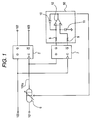
- Fig. 1 is a configuration block diagram showing an embodiment of a phase control circuit according to the present invention.
- reference numerals 2, 100, 101, 101a, 102, and 103 are the same as those shown in Fig. 6.
- Reference numeral 6 designates a variable delay circuit;
- reference numeral 7 designates a flip-flop circuit;
- reference numerals 8 and 9 designate resistors;
- reference numerals 10 and 11 designate capacitors;
- reference numeral 12 designates an amplifier.
- An integration circuit 50 includes the resistors 8 and 9, the capacitors 10 and 11, and the amplifier 12.
- the data signal 100 is transmitted to a data input terminal of the flip-flop circuit 2 and a clock input terminal of the flip-flop circuit 7.
- the clock signal 101 is transmitted to an input terminal of the variable delay circuit 6, and an output terminal of the variable-delay circuit 6 is connected to a clock input terminal of the flip-flop circuit 2 and a data input terminal of the flip-flop circuit 7.
- a noninverted output terminal of the flip-flop circuit 7 is connected to one end of the resistor 8, and the other end of the resistor 8 is connected to one end of the capacitor 10 and an inverted input terminal of the amplifier 12.
- An inverted output terminal of the flip-flop circuit 7 is connected to one end of the resistor 9, and the other end of the resistor 9 is connected to one end of the capacitor 11 and a noninverted input terminal of the amplifier 12.
- the other end of the capacitor 11 is connected to ground, and an output terminal of the amplifier 12 is connected to a control terminal of the variable delay circuit 6 and the other end of the capacitor 10.
- the noninverted output signal 102 is output from the noninverted output terminal of the flip-flop circuit 2, and the inverted output signal 103 is output from an inverted output terminal of the flip-flop circuit 2.
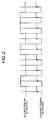
- Fig. 2 is a timing chart showing an operation timing of the flip-flop circuit 2
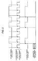
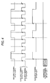
- Figs. 3 and 4 are timing charts showing the operation timing of the flip-flop circuit 2 and that of the flip-flop circuit 7.
- Fig. 2 shows a timing chart achieved when the timing of data input and the timing of a clock signal input to the flip-flop circuit 2 are optimal. Specifically, the timing of a rising edge of the clock signal 101a does not coincide with the timing of change in the data signal 100 but the timing comes when the data signal is stable.
- Fig. 3 shows a timing chart achieved when the timing of data input to the flip-flop circuit 2 is ahead of the optimal timing.
- the noninverted output signal of the flip-flop circuit 7 becomes constantly at a low level except an initial unstable period, whereas the inverted output signal becomes constantly at a high level except the initial unstable period.
- variable delay circuit 6 the delay amount changes in accordance with the magnitude of a control signal that is input to a control terminal of the variable delay circuit. Specifically, when the control signal is large, the delay amount becomes larger. In contrast, when the control signal is small, the delay amount becomes smaller.
- the delay amount of the variable delay circuit 6 gradually becomes larger correspondingly. Then, the clock signal 101a having been input ahead of the optimal timing approaches the optimal timing.
- Fig. 4 shows a timing chart achieved when the timing of data input to the flip-flop circuit 2 is behind the optimal timing. As shown in Fig. 4, the noninverted output signal from the flip-flop circuit 7 becomes constantly at a high level except the initial unstable period, and the inverted output signal becomes constantly at a low level except the initial unstable period.
- the delay amount of the variable delay circuit 6 gradually becomes smaller correspondingly. Then, the clock signal 101a having been input behind the optimal timing approaches the optimal timing.
- the integration circuit 50 integrates outputs from the flip-flop circuit 7 having the clock input terminal to which the data signal 100 is input and the data input terminal to which the clock signal 101a is input. Then, the variable delay circuit 6 is controlled based on the integrated output, whereby the timing of the clock signal 101 is optimized. Accordingly, the adjustment to obtain the optimal timing is available at all times regardless to changes over time or temperature changes.
- the integration circuit 50 is provided with a differential input configuration.
- providing the integration circuit with a differential input configuration is not always needed, and the integration circuit may also be provided with a single input configuration.
- the integration circuit 50 is formed with electrical components.
- forming the integration circuit with the electrical components is not always necessary, and integration may also be performed by use of a mechanical component such as a motor.
- Fig. 5 is a configuration block diagram showing another embodiment of the phase control circuit of the present invention.
- reference numerals 2, 7, 100, 101, 101a, 102, and 103 are the same as those shown in Fig. 1.
- Reference numeral 6a designates a variable delay circuit;
- reference numeral 13 designates a motor driving circuit;
- reference numeral 14 designates a motor.
- An integration circuit 51 includes the motor driving circuit 13 and the motor 14.
- a noninverted output terminal of the flip-flop circuit 7 is connected to one input terminal of the motor driving circuit 13, and an inverted output terminal of the flip-flop circuit 7 is connected to the other input terminal of the motor driving circuit 13.
- One output terminal of the motor driving circuit 13 is connected to one input terminal of the motor 14, and the other output terminal of the motor driving circuit 13 is connected to the other input terminal of the motor 14.
- a rotary portion of the motor 14 is connected to a delay control rotary switch of the variable delay circuit 6a.
- the other connections are the same as those shown in Fig. 1, and hence their explanations are omitted.
- phase control circuit The basic operation of the phase control circuit is essentially identical with that of the phase control circuit according to the embodiment shown in Fig. 1. A difference between the basic operations of the phase control circuits lies in that the integration circuit 51 is formed with the motor driving circuit 13 and the motor 14, and that the variable delay circuit 6a is controlled by mechanical driving force.
- the noninverted output signal of the flip-flop circuit 7 remains at a low level at all times except the initial unstable period, whereas the inverted output signal remains at a high level at all times except the initial unstable period.
- the motor driving circuit 13 rotates the motor 14 at a given speed in one direction.
- the delay control rotary switch of the variable delay circuit 6a is rotated, and the delay amount gradually becomes large.
- the clock signal 101a having been input ahead of the optimal timing approaches the optimal timing.
- the noninverted output signal of the flip-flop circuit 7 remains at a high level at all times except the initial unstable period, whereas the inverted output signal of the same remains at a low level at all times except the initial unstable period.
- the motor driving circuit 13 rotates the motor 14 at a given speed in reverse direction.
- the delay control rotary switch of the variable delay circuit 6a is rotated, and the delay amount gradually becomes small.
- the clock signal 101a having been input behind the optimal timing approaches the optimal timing.
- the data signal 100 is input to the clock input terminal, the integration circuit 51 converts, into mechanical rotation, outputs from the flip-flop circuit 7 having the data input terminal to which the clock signal 101a is input. Then, the variable delay circuit 6a is controlled based on the mechanical rotation.
- the timing of the clock signal 101 is optimized. Accordingly, the adjustment to obtain the optimal timing is available at all times regardless to changes over time or temperature changes.
- variable delay circuit 6a is controlled by the rotation generated by the integration circuit 51.
- rotation is not always needed, and the variable delay circuit 6a may be controlled by any mechanical driving force.
- the rotation generated by the integration circuit 51 may be converted into horizontal sliding motion, and the delay amount of the variable delay circuit 6a may also be switched by a slide switch.
Landscapes
- Engineering & Computer Science (AREA)
- Computer Networks & Wireless Communication (AREA)
- Signal Processing (AREA)
- Pulse Circuits (AREA)
- Manipulation Of Pulses (AREA)
- Stabilization Of Oscillater, Synchronisation, Frequency Synthesizers (AREA)
Applications Claiming Priority (1)
| Application Number | Priority Date | Filing Date | Title |
|---|---|---|---|
| JP2006026667A JP2007208774A (ja) | 2006-02-03 | 2006-02-03 | 位相制御回路 |
Publications (1)
| Publication Number | Publication Date |
|---|---|
| EP1816748A1 true EP1816748A1 (de) | 2007-08-08 |
Family
ID=38006843
Family Applications (1)
| Application Number | Title | Priority Date | Filing Date |
|---|---|---|---|
| EP07001984A Withdrawn EP1816748A1 (de) | 2006-02-03 | 2007-01-30 | Phasenregelschaltung |
Country Status (3)
| Country | Link |
|---|---|
| US (1) | US20080001641A1 (de) |
| EP (1) | EP1816748A1 (de) |
| JP (1) | JP2007208774A (de) |
Cited By (1)
| Publication number | Priority date | Publication date | Assignee | Title |
|---|---|---|---|---|
| EP3041136A1 (de) * | 2014-12-31 | 2016-07-06 | Semtech Corporation | Halbleiterbauelement und verfahren zur genauen taktdomänensynchronisation über einen grossen frequenzbereich |
Families Citing this family (2)
| Publication number | Priority date | Publication date | Assignee | Title |
|---|---|---|---|---|
| US9337817B2 (en) | 2014-06-17 | 2016-05-10 | Via Alliance Semiconductor Co., Ltd. | Hold-time optimization circuit and receiver with the same |
| US10642923B2 (en) * | 2015-04-01 | 2020-05-05 | Micro Focus Llc | Graphs with normalized actual value measurements and baseline bands representative of normalized measurement ranges |
Citations (2)
| Publication number | Priority date | Publication date | Assignee | Title |
|---|---|---|---|---|
| WO2001090864A2 (en) * | 2000-05-22 | 2001-11-29 | Igor Anatolievich Abrosimov | Timing control means for automatic compensation of timing uncertainties |
| US6389090B2 (en) * | 1998-02-06 | 2002-05-14 | 3Com Corporation | Digital clock/data signal recovery method and apparatus |
Family Cites Families (3)
| Publication number | Priority date | Publication date | Assignee | Title |
|---|---|---|---|---|
| US6674387B1 (en) * | 2002-10-02 | 2004-01-06 | Honeywell International Inc. | Pulse width modulation analog to digital conversion |
| US7009456B2 (en) * | 2003-08-04 | 2006-03-07 | Agere Systems Inc. | PLL employing a sample-based capacitance multiplier |
| US7274231B1 (en) * | 2005-09-15 | 2007-09-25 | Integrated Device Technology, Inc. | Low jitter frequency synthesizer |
-
2006
- 2006-02-03 JP JP2006026667A patent/JP2007208774A/ja active Pending
-
2007
- 2007-01-30 EP EP07001984A patent/EP1816748A1/de not_active Withdrawn
- 2007-02-02 US US11/701,398 patent/US20080001641A1/en not_active Abandoned
Patent Citations (2)
| Publication number | Priority date | Publication date | Assignee | Title |
|---|---|---|---|---|
| US6389090B2 (en) * | 1998-02-06 | 2002-05-14 | 3Com Corporation | Digital clock/data signal recovery method and apparatus |
| WO2001090864A2 (en) * | 2000-05-22 | 2001-11-29 | Igor Anatolievich Abrosimov | Timing control means for automatic compensation of timing uncertainties |
Cited By (2)
| Publication number | Priority date | Publication date | Assignee | Title |
|---|---|---|---|---|
| EP3041136A1 (de) * | 2014-12-31 | 2016-07-06 | Semtech Corporation | Halbleiterbauelement und verfahren zur genauen taktdomänensynchronisation über einen grossen frequenzbereich |
| US9577648B2 (en) | 2014-12-31 | 2017-02-21 | Semtech Corporation | Semiconductor device and method for accurate clock domain synchronization over a wide frequency range |
Also Published As
| Publication number | Publication date |
|---|---|
| US20080001641A1 (en) | 2008-01-03 |
| JP2007208774A (ja) | 2007-08-16 |
Similar Documents
| Publication | Publication Date | Title |
|---|---|---|
| EP1146644B1 (de) | Verfahren und Schaltung zum Korrigieren des Tastverhältnisses eines Signals | |
| KR100319890B1 (ko) | 지연동기루프 및 이에 대한 제어방법 | |
| EP1748562B1 (de) | Schaltung und Verfahren zur Erzeugung eines Taktsignals | |
| EP1816748A1 (de) | Phasenregelschaltung | |
| JP4484629B2 (ja) | クロックデータリカバリ回路及び電圧制御発振回路 | |
| TWI681634B (zh) | 時脈資料回復電路 | |
| US5365130A (en) | Self-compensating output pad for an integrated circuit and method therefor | |
| EP3687070B1 (de) | Takt- und datenwiederherstellung und zugehöriges signalverarbeitungsverfahren | |
| US12512841B2 (en) | Data reception device based on low-power digital delay-locked loop having skew correction function | |
| US4713690A (en) | Sampling clock phase correction circuit of video signal | |
| US5608343A (en) | Circuit for varying read timing | |
| US6937953B2 (en) | Circuit configuration for receiving at least two digital signals | |
| US7872515B1 (en) | Phase interpolation device and slew rate control device thereof | |
| US7760839B2 (en) | Offset controllable spread spectrum clock generator apparatus | |
| US7092471B2 (en) | Digital phase synchronization circuit | |
| US6249556B1 (en) | Dynamic thresholding for input receivers | |
| CN115085894B (zh) | 信号同步系统 | |
| TWI746295B (zh) | 時鐘和資料恢復電路及其信號處理方法 | |
| US12456982B2 (en) | Clock and data recovery device | |
| US12206420B2 (en) | Duty cycle monitoring method and apparatus for memory interface | |
| JP2002314518A (ja) | 位相比較回路及び光受信装置 | |
| JP2001186017A (ja) | Pll回路 | |
| JP3209211B2 (ja) | 位相同期回路 | |
| US8019033B2 (en) | Data transmission system, controller, and its method | |
| KR100885486B1 (ko) | 반도체 메모리 장치 |
Legal Events
| Date | Code | Title | Description |
|---|---|---|---|
| PUAI | Public reference made under article 153(3) epc to a published international application that has entered the european phase |
Free format text: ORIGINAL CODE: 0009012 |
|
| AK | Designated contracting states |
Kind code of ref document: A1 Designated state(s): AT BE BG CH CY CZ DE DK EE ES FI FR GB GR HU IE IS IT LI LT LU LV MC NL PL PT RO SE SI SK TR |
|
| AX | Request for extension of the european patent |
Extension state: AL BA HR MK YU |
|
| AKX | Designation fees paid | ||
| STAA | Information on the status of an ep patent application or granted ep patent |
Free format text: STATUS: THE APPLICATION IS DEEMED TO BE WITHDRAWN |
|
| 18D | Application deemed to be withdrawn |
Effective date: 20080209 |
|
| REG | Reference to a national code |
Ref country code: DE Ref legal event code: 8566 |