EP1818430A1 - Simple cristal de nitrure du groupe iii et procédé de préparation dudit cristal, et dispositif à semi-conducteur - Google Patents
Simple cristal de nitrure du groupe iii et procédé de préparation dudit cristal, et dispositif à semi-conducteur Download PDFInfo
- Publication number
- EP1818430A1 EP1818430A1 EP05759959A EP05759959A EP1818430A1 EP 1818430 A1 EP1818430 A1 EP 1818430A1 EP 05759959 A EP05759959 A EP 05759959A EP 05759959 A EP05759959 A EP 05759959A EP 1818430 A1 EP1818430 A1 EP 1818430A1
- Authority
- EP
- European Patent Office
- Prior art keywords
- iii nitride
- crystal
- layer
- substrate
- liquid
- Prior art date
- Legal status (The legal status is an assumption and is not a legal conclusion. Google has not performed a legal analysis and makes no representation as to the accuracy of the status listed.)
- Granted
Links
Images

Classifications
-
- C—CHEMISTRY; METALLURGY
- C30—CRYSTAL GROWTH
- C30B—SINGLE-CRYSTAL GROWTH; UNIDIRECTIONAL SOLIDIFICATION OF EUTECTIC MATERIAL OR UNIDIRECTIONAL DEMIXING OF EUTECTOID MATERIAL; REFINING BY ZONE-MELTING OF MATERIAL; PRODUCTION OF A HOMOGENEOUS POLYCRYSTALLINE MATERIAL WITH DEFINED STRUCTURE; SINGLE CRYSTALS OR HOMOGENEOUS POLYCRYSTALLINE MATERIAL WITH DEFINED STRUCTURE; AFTER-TREATMENT OF SINGLE CRYSTALS OR A HOMOGENEOUS POLYCRYSTALLINE MATERIAL WITH DEFINED STRUCTURE; APPARATUS THEREFOR
- C30B19/00—Liquid-phase epitaxial-layer growth
- C30B19/02—Liquid-phase epitaxial-layer growth using molten solvents, e.g. flux
- C30B19/04—Liquid-phase epitaxial-layer growth using molten solvents, e.g. flux the solvent being a component of the crystal composition
-
- C—CHEMISTRY; METALLURGY
- C30—CRYSTAL GROWTH
- C30B—SINGLE-CRYSTAL GROWTH; UNIDIRECTIONAL SOLIDIFICATION OF EUTECTIC MATERIAL OR UNIDIRECTIONAL DEMIXING OF EUTECTOID MATERIAL; REFINING BY ZONE-MELTING OF MATERIAL; PRODUCTION OF A HOMOGENEOUS POLYCRYSTALLINE MATERIAL WITH DEFINED STRUCTURE; SINGLE CRYSTALS OR HOMOGENEOUS POLYCRYSTALLINE MATERIAL WITH DEFINED STRUCTURE; AFTER-TREATMENT OF SINGLE CRYSTALS OR A HOMOGENEOUS POLYCRYSTALLINE MATERIAL WITH DEFINED STRUCTURE; APPARATUS THEREFOR
- C30B13/00—Single-crystal growth by zone-melting; Refining by zone-melting
- C30B13/02—Zone-melting with a solvent, e.g. travelling solvent process
-
- C—CHEMISTRY; METALLURGY
- C30—CRYSTAL GROWTH
- C30B—SINGLE-CRYSTAL GROWTH; UNIDIRECTIONAL SOLIDIFICATION OF EUTECTIC MATERIAL OR UNIDIRECTIONAL DEMIXING OF EUTECTOID MATERIAL; REFINING BY ZONE-MELTING OF MATERIAL; PRODUCTION OF A HOMOGENEOUS POLYCRYSTALLINE MATERIAL WITH DEFINED STRUCTURE; SINGLE CRYSTALS OR HOMOGENEOUS POLYCRYSTALLINE MATERIAL WITH DEFINED STRUCTURE; AFTER-TREATMENT OF SINGLE CRYSTALS OR A HOMOGENEOUS POLYCRYSTALLINE MATERIAL WITH DEFINED STRUCTURE; APPARATUS THEREFOR
- C30B29/00—Single crystals or homogeneous polycrystalline material with defined structure characterised by the material or by their shape
- C30B29/10—Inorganic compounds or compositions
- C30B29/40—AIIIBV compounds wherein A is B, Al, Ga, In or Tl and B is N, P, As, Sb or Bi
- C30B29/403—AIII-nitrides
-
- C—CHEMISTRY; METALLURGY
- C30—CRYSTAL GROWTH
- C30B—SINGLE-CRYSTAL GROWTH; UNIDIRECTIONAL SOLIDIFICATION OF EUTECTIC MATERIAL OR UNIDIRECTIONAL DEMIXING OF EUTECTOID MATERIAL; REFINING BY ZONE-MELTING OF MATERIAL; PRODUCTION OF A HOMOGENEOUS POLYCRYSTALLINE MATERIAL WITH DEFINED STRUCTURE; SINGLE CRYSTALS OR HOMOGENEOUS POLYCRYSTALLINE MATERIAL WITH DEFINED STRUCTURE; AFTER-TREATMENT OF SINGLE CRYSTALS OR A HOMOGENEOUS POLYCRYSTALLINE MATERIAL WITH DEFINED STRUCTURE; APPARATUS THEREFOR
- C30B7/00—Single-crystal growth from solutions using solvents which are liquid at normal temperature, e.g. aqueous solutions
-
- C—CHEMISTRY; METALLURGY
- C30—CRYSTAL GROWTH
- C30B—SINGLE-CRYSTAL GROWTH; UNIDIRECTIONAL SOLIDIFICATION OF EUTECTIC MATERIAL OR UNIDIRECTIONAL DEMIXING OF EUTECTOID MATERIAL; REFINING BY ZONE-MELTING OF MATERIAL; PRODUCTION OF A HOMOGENEOUS POLYCRYSTALLINE MATERIAL WITH DEFINED STRUCTURE; SINGLE CRYSTALS OR HOMOGENEOUS POLYCRYSTALLINE MATERIAL WITH DEFINED STRUCTURE; AFTER-TREATMENT OF SINGLE CRYSTALS OR A HOMOGENEOUS POLYCRYSTALLINE MATERIAL WITH DEFINED STRUCTURE; APPARATUS THEREFOR
- C30B7/00—Single-crystal growth from solutions using solvents which are liquid at normal temperature, e.g. aqueous solutions
- C30B7/005—Epitaxial layer growth
-
- C—CHEMISTRY; METALLURGY
- C30—CRYSTAL GROWTH
- C30B—SINGLE-CRYSTAL GROWTH; UNIDIRECTIONAL SOLIDIFICATION OF EUTECTIC MATERIAL OR UNIDIRECTIONAL DEMIXING OF EUTECTOID MATERIAL; REFINING BY ZONE-MELTING OF MATERIAL; PRODUCTION OF A HOMOGENEOUS POLYCRYSTALLINE MATERIAL WITH DEFINED STRUCTURE; SINGLE CRYSTALS OR HOMOGENEOUS POLYCRYSTALLINE MATERIAL WITH DEFINED STRUCTURE; AFTER-TREATMENT OF SINGLE CRYSTALS OR A HOMOGENEOUS POLYCRYSTALLINE MATERIAL WITH DEFINED STRUCTURE; APPARATUS THEREFOR
- C30B9/00—Single-crystal growth from melt solutions using molten solvents
- C30B9/04—Single-crystal growth from melt solutions using molten solvents by cooling of the solution
- C30B9/06—Single-crystal growth from melt solutions using molten solvents by cooling of the solution using as solvent a component of the crystal composition
Definitions
- the present invention relates to methods of manufacturing Group III nitride single crystals utilized in semiconductor devices such as light-emitting diodes, electronic circuit elements, and semiconductor sensors.
- the invention relates to a method of manufacturing III nitride single crystals efficiently and at favorable yields.
- III nitride single crystals have extraordinary utility as materials to create substrates for light-emitting diodes, electronic circuit elements, and semiconductor sensors.
- Non-Patent Document 1 As well as by liquid-phase techniques such as high nitrogen pressure growth or the flux method-for example, reference is made to Patent Document 1 and Non-Patent Document 2.
- HVPE hydride vapor-phase epitaxy
- MOCVD metalorganic chemical vapor deposition
- the source material yield is on the order of an extremely low 1%.
- Patent Document 1 Japanese Unexamined Pat. App. Pub. No. 2001-58900 .
- Patent Document 2 Japanese Unexamined Pat. App. Pub. No. 2002-47100 .
- Non-Patent Document 1 H.
- Non-Patent Document 2 H. Yamane et al., "GaN Single Crystal Growth by the Flux Method,” Applied Physics, The Japan Society of Applied Physics, 2002, Vol. 71, No. 5, pp. 548-552 .
- An object of the present invention is to make available a III nitride single-crystal manufacturing method whereby yields from the source materials are high and the crystal growth rate is advanced. This means that in order to manufacture III nitride single crystal at high yield and an advanced crystal growth rate, the problem becomes how to transport the Group-III element atoms and the nitrogen atoms efficiently.
- the present invention is a method of manufacturing III nitride single crystal, in which a liquid layer 200 ⁇ m or less in thickness is formed in between a substrate and a III nitride source-material baseplate, and III nitride single crystal is grown onto the face of the substrate on its liquid-layer side.
- the substrate in at least a superficial layer along the liquid layer can be formed of a III nitride single crystal, while the III nitride source-material baseplate can be formed of a III nitride polycrystal.
- the substrate in at least a superficial layer along the liquid layer, and the III nitride source-material baseplate can be formed of a III nitride single crystal, while the face of the substrate on its liquid-layer side can be made a Group-III-atom surface, and the face of the III nitride source-material baseplate on its liquid-layer side can be made a nitrogen-atom surface.
- an element of at least one kind selected from the group consisting of elements constituting the III nitride single crystal can be included in the liquid layer.
- the present invention is a III nitride single crystal obtained according to the foregoing III nitride single-crystal manufacturing method.
- the present invention is a semiconductor device that incorporates an above-recited III nitride single crystal.
- the present invention affords a III nitride single-crystal manufacturing method by which yields from the source materials are high and the crystal growth rate is advanced.
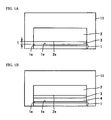
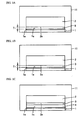
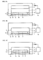
- 1 substrate; 1a: superficial layer; 1s, 2s: faces; 2: III nitride source-material baseplate; 3: liquid layer; 4: III nitride single crystal; 5: solid layer; 11: crystal growth chamber; 12: spacer; 13: interspace; 14: vacuum pump; 20: III nitride layer; 21: III nitride single-crystal substrate; 22: n - type GaN layer; 23: In 0.2 Ga 0.8 N layer; 24: Al 0.2 Ga 0.8 N layer; 25: p -type GaN layer; 31: n - side electrode; 32: p - side electrode; 40: semiconductor device; 45: emitted light.
- a liquid layer 3 of 200 ⁇ m or less thickness is formed in between the substrate 1 and the III nitride source-material baseplate 2, and as indicated in Fig. 1B, III nitride single crystal 4 is grown onto the face 1s of the substrate 1 on its liquid-layer side.
- III elements and nitrogen elements within the III nitride source-material baseplate 2 dissolve out of the face 2s of the III nitride source-material baseplate 2 on its liquid-layer side and into the liquid layer 3, and are transported by the liquid layer 3 to the face 1s of the substrate 1 on its liquid-layer side, causing III nitride single crystal 4 to grow onto the substrate 1.
- the source-material yield is enhanced. What is more, because the thickness of the liquid layer is an extremely thin 200 ⁇ m or less, the nitrogen transport is not the rate-determining step; rather, the growth speed is determined by the dissolving out of nitrogen from the III nitride source-material baseplate 2, on account of which the crystal-growth rate of the III nitride single crystal is heightened.
- the substrate 1 in at least a superficial layer 1a along the liquid layer be formed of a III nitride single crystal, and that the III nitride source-material baseplate 2 be formed of a III nitride polycrystal.
- III nitride single crystal Forming the substrate 1 of a III nitride single crystal in at least a superficial layer 1a on the substrate's liquid-layer side, and growing the same type of a III nitride single crystal onto the face 1s of the substrate 1 on its liquid-layer side, yields large III nitride single crystal of favorable crystallinity.
- III nitride single crystal at least a liquid-layer-side, superficial layer 1a of the substrate 1, and forming of a III nitride polycrystal the III nitride source-material baseplate 2 makes the face 1s of the substrate 1 on its liquid layer side a III nitride single-crystal surface, and the face 2s of the III nitride source-material baseplate 2 on its liquid layer side a III nitride polycrystal.
- the surface energy of the III nitride polycrystal surface is higher than that of the III nitride single-crystal surface, the transport of III nitride source material from the liquid-layer-ward face 2s of the III nitride source-material baseplate 2 to the liquid-layer-ward face 1s of the substrate 1 is promoted.
- the superficial layer 1a of the substrate 1 along its liquid-layer side, and the III nitride source-material baseplate 2 be formed of a III nitride single crystal, and that the liquid-layer-ward face 1s of the substrate 1 be made a Group-III-atom surface, and the liquid-layer-ward face 2s of the III nitride source-material baseplate 2 be made a nitrogen-atom surface.
- III-atom surface means the planar surface wherein the atoms of the Group-III element that forms the III nitride single crystal are arrayed in a single plane, which is equivalent to the (0001) crystallographic plane in a hexagonal III nitride single-crystal system, and to the (111) plane in a cubic III nitride single-crystal system.
- a "nitrogen atom surface” means the planar surface wherein the nitrogen atoms that form the III nitride single crystal are arrayed in a single plane, which is equivalent to the (000 1 ⁇ ) crystallographic plane in a hexagonal III nitride single-crystal system, and to the 1 ⁇ 1 ⁇ 1 ⁇ plane in a cubic III nitride single-crystal system.
- the liquid layer 3 is not particularly limited as long as it promotes transport of III nitride source material, but preferably contains at least an element of a single kind selected from the group consisting of elements that form III nitride single crystal. Including at least an element of a single kind among elements that form III nitride single crystal makes for promoting the transport of the III nitride source material.
- the liquid layer preferably contains Al, alumina (Al 2 O 3 ), a composite compound of a rare-earth oxide and alumina ( R 2 O 3 -Al 2 O 3 , wherein R indicates a rare-earth element), or the like.
- the liquid layer preferably contains Ga or the like.
- the liquid layer preferably contains Al and/or Ga, or the like.
- the layer, 200 ⁇ m or less in thickness, in between the substrate 1 and the III nitride source-material baseplate 2 is formed from the perspective of ease of forming the liquid layer 3, the two methods below are preferably utilized.
- the first method is as follows. First, with reference to Fig. 2A, a solid layer 5 of thickness T 1 that liquefies to become the liquid layer 3 is formed onto the face 2s of the III nitride source-material baseplate 2, and the III nitride source-material baseplate 2 on which the solid layer 5 has been formed is set onto the substrate 1, which has been placed within a crystal-growth chamber 11, such that the solid layer 5 contacts the face 1s of the substrate 1. Alternatively, a solid layer 5 of thickness T 1 that liquefies on the face 1s of the substrate 1 to become the liquid layer 3 is formed onto that face 1s, and the III nitride source-material baseplate 2 is set onto the solid layer 5.
- the solid layer 5 of thickness T 1 is formed onto the III nitride source-material baseplate 2 or the substrate 1, from the perspective of ease of forming the solid layer 5, sputtering, vapor deposition, or a similar technique is preferably utilized.
- the crystal-growth chamber 11 is heated to liquefy the above-described solid layer 5, whereby a liquid layer 3 of thickness T 1 is formed in between the substrate 1 and the III nitride source-material baseplate 2. Then, with reference to Fig. 2C, the crystal-growth chamber 11 is maintained at a predetermined temperature (crystal-growth temperature) for a predetermined time period (crystal-growth time period), to enable III nitride single crystal 4 to be grown onto the liquid-layer-ward face 1s of the substrate 1.
- a predetermined temperature crystal-growth temperature
- time period predetermined time period
- This method is one that preferably is utilized with the thickness of the liquid layer being not greater than 50 ⁇ m, more preferably 30 ⁇ m or less. If the liquid-layer thickness exceeds 50 ⁇ m, the liquid layer 3 escapes from between the substrate 1 and the III nitride source-material baseplate 2, making it difficult to keep the thickness of the liquid layer 3 constant and making it difficult to control the growth speed of the III nitride single crystal.
- the second method is as follows. First, referring to Fig. 3A, with spacers 12 of thickness T 2 interposing in, for example, four sites that evenly divide the peripheral top on a substrate 1 placed in the crystal-growth chamber 11, a III nitride source-material baseplate 2 is set atop the spacers 12, and a solid layer 5 that liquefies to become a liquid layer 3 is set atop the III nitride source-material baseplate 2. Accordingly, in this situation, an interspace 13 is formed in between the substrate 1 and the III nitride source-material baseplate 2, separating the two by T 2 .
- a vacuum pump 14 is arranged on the crystal-growth chamber 11.
- the crystal-growth chamber 11 is heated and at the same time pumped down to a vacuum with the vacuum pump 14, whereby the solid layer 5 liquefies to form the liquid layer 3, and the liquid layer 3 spreads into every nook and cranny of the interspace 13, forming a liquid layer 3 of thickness T 2 in between the substrate 1 and the III nitride source-material baseplate 2.
- the crystal-growth chamber 11 is maintained at a predetermined temperature (crystal-growth temperature) for a predetermined time period (crystal-growth time period), to enable III nitride single crystal 4 to be grown onto the liquid-layer-ward face 1s of the substrate 1.
- the level in the crystal-growth chamber 11 interior although not particularly limited as long as it is sufficient for the liquid layer 3 to spread throughout the interspace 13, the level can be put at for example 1 kPa (0.01 atm) or less.
- Advantages to this method are that it enables a liquid layer whose thickness is 50 ⁇ m or more to be readily formed, and that it allows the thickness of the liquid layer to be freely determined according to the thickness of the spacers.
- III nitride single crystal involving the present invention is obtained by means of an above-described method of manufacturing III nitride single crystal.
- a semiconductor device involving the present invention is a device that incorporates an above-described III nitride single crystal.
- a III nitride single crystal described above is incorporated into a semiconductor device as, for example, a III nitride single-crystal substrate.
- one semiconductor device involving the present invention is, referring to Fig. 4, a semiconductor device in which an n - type GaN layer 22, an In 0.2 Ga 0.8 N layer 23, an Al 0.2 Ga 0.8 N layer 24, and a p -type GaN layer 25 are formed in that order onto a III nitride single-crystal substrate 21, and an n-side electrode 31 is formed on the undersurface of the III nitride single-crystal substrate 21, and a p - side electrode 32 is formed on the top surface of the p -type GaN layer 25.
- an Al metal layer 10 ⁇ m in thickness was formed onto one of the sides of the III nitride source-material baseplate 2 by sputtering.
- the III nitride source-material baseplate 2 on which the solid layer 5 had been formed was set onto the substrate 1, which had been placed in a crucible or similar crystal-growth chamber 11, so as to bring the solid layer 5 into contact with the AIN single-crystal layer on the substrate 1.
- the crystal-growth chamber 11 was heated to liquefy the Al metal layer, i.e., the solid layer 5, whereby a molten Al layer, i.e., the liquid layer 3, of 10 ⁇ m thickness was formed in between the substrate 1 and the III nitride source-material baseplate 2.
- the crystal-growth chamber 11 was heated to 1800°C (crystal-growth temperature) and maintained there for 3 hours (crystal-growth time period), whereby AlN single crystal, i.e., III nitride single crystal 4, of 90 ⁇ m thickness was grown onto the liquid-layer-ward face 1s of the substrate 1.
- the crystal growth rate was 30 ⁇ m/h. It should be noted that single crystal from the embodiments in the present application was confirmed to be monocrystalline by X-ray diffraction analysis (XRD). The results are tabulated in the table.
- spacers 12 of 35 nm thickness were set in, for example, 4 sites that evenly divide the peripheral top on the substrate 1, which had been placed in the crystal-growth chamber 11, the III nitride source-material baseplate 2 was set atop the spacers 12, and Al metal as a solid layer 5 that liquefies into a liquid layer 3 was set atop the III nitride source - material baseplate 2.
- an interspace 13 was formed in between the substrate 1 and the III nitride source-material baseplate 2, separating the two by 35 nm.
- the crystal-growth chamber 11 was heated to 1000°C and at the same time pumped down to 1 kPa (0.01 atm) with the vacuum pump 14, whereby the Al metal, i.e., the solid layer 5, liquefied to form a liquid layer 3 of molten Al, and the liquid layer 3 spread into every nook and cranny of the interspace 13, forming a molten Al layer (liquid layer 3) of 35 nm thickness in between the substrate 1 and the III nitride source-material baseplate 2.
- the Al metal i.e., the solid layer 5
- the crystal-growth chamber 11 was heated to 1800°C and maintained there for 3 hours, whereby AlN single crystal, i.e., III nitride single crystal 4, of 27 ⁇ m thickness was grown onto the liquid-layer-ward face 1s of the substrate 1.
- the crystal growth rate was 9 ⁇ m/h. The results are tabulated in the table.
- AlN single crystal 16 ⁇ m in thickness was grown in a manner similar to that of Embodiment 2, except that the separation (equal to the thickness of the liquid layer-ditto in the following) between the substrate and III nitride source-material baseplate was made 150 ⁇ m, the crystal-growth temperature 2100°C, and the crystal-growth time period 4 hours. The crystal growth rate was 4 ⁇ m/h. The results are tabulated in the table.
- AIN crystal 36 ⁇ m in thickness was grown in a manner similar to that of Embodiment 1, except that the separation between the substrate and III nitride source-material baseplate was made 22 ⁇ m, and the crystal-growth time period 2 hours.
- the crystal growth rate was 18 ⁇ m/h. The results are tabulated in the table.
- a substrate 1 and, as a III nitride source-material baseplate 2, a hexagonal GaN single-crystal plate of 15 mm diameter x 350 ⁇ m thickness were prepared, and an Na metal layer 10 ⁇ m in thickness was formed as a solid layer 5 onto the nitrogen-atom surface ((000 1 ⁇ ) face) of the III nitride source-material baseplate 2 by sputtering.
- the III nitride source-material baseplate 2 on which the solid layer 5 had been formed was set onto the III-element surface ((0001) face) of the substrate 1, which had been placed in a crucible or similar crystal-growth chamber 11, so as to bring the solid layer 5 into contact with the III-element surface ((0001) face) of the substrate 1.
- the crystal-growth chamber 11 was heated to liquefy the Na metal layer, i.e., the solid layer 5, whereby a molten Na layer, i.e., the liquid layer 3, of 10 ⁇ m thickness was formed in between the substrate 1 and the III nitride source-material baseplate 2.
- the crystal-growth chamber 11 was heated to 800°C and maintained there for 2 hours, whereby GaN single crystal, i.e., III nitride single crystal 4, of 30 ⁇ m thickness was grown onto the liquid-layer-ward face 1s (III-atom face, (0001) face) of the substrate 1.
- the crystal growth rate was 15 ⁇ m/h.
- a substrate 1 and, as a III nitride source-material baseplate 2, a hexagonal GaN single-crystal plate of 15 mm diameter x 350 ⁇ m thickness were prepared.
- spacers 12 of 20 nm thickness were set in, for example, 4 sites that evenly divide the peripheral top of the Group III element atom surface (Ga face, (0001) face) of the substrate 1, which had been placed in the crystal-growth chamber 11, the III nitride source-material baseplate 2 was set atop the spacers 12 such that the nitrogen-atom surface (N face, (0001) face) of the III nitride source-material baseplate 2 opposed the substrate 1 surface of Group III element atoms (Ga face, (0001) face), and Ga metal as a solid layer 5 that liquefies into a liquid layer 3 was set atop the III nitride source-material baseplate 2.
- an interspace 13 was formed in between the substrate 1 and the III
- the crystal-growth chamber 11 was heated to 300°C and at the same time pumped down to 1 kPa (0.01 atm) with the vacuum pump 14, whereby the Ga metal, i.e., the solid layer 5, liquefied to form a liquid layer 3 of molten Ga, and the liquid layer 3 spread into every nook and cranny of the interspace 13, forming a molten Ga layer (liquid layer 3) of 20 nm thickness in between the substrate 1 and the III nitride source-material baseplate 2.
- the Ga metal i.e., the solid layer 5
- the crystal-growth chamber 11 was heated to 800°C and maintained there for 6 hours, whereby GaN single crystal, i.e., III nitride single crystal 4, of 48 ⁇ m thickness was grown onto the liquid-layer-ward face 1s of the substrate 1.
- the crystal growth rate was 8 ⁇ m/h. The results are tabulated in the table.
- a layer 20 ⁇ m in thickness of a Na-Al-Ga metal alloy (at 5 : 2 : 3 mass ratios) was formed onto one of the sides of the substrate 1 by sputtering.
- the crystal-growth chamber 11 was heated to liquefy the Na-Al-Ga metal alloy layer, i.e., the solid layer 5, whereby a molten Na-Al-Ga layer, i.e., a liquid layer 3, of 20 ⁇ m thickness was formed in between the substrate 1 and the III nitride source-material baseplate 2.
- the crystal-growth chamber 11 was heated to 800°C (crystal-growth temperature) and maintained there for 6 hours (crystal-growth time period), whereby AlN single crystal, i.e., III nitride single crystal 4, of 54 ⁇ m thickness was grown onto the liquid-layer-ward face 1s of the substrate 1.
- the crystal growth rate was 90 ⁇ m/h. The results are tabulated in the table.
- A1N crystal was grown in a manner similar to that of Embodiment 1, except that the separation between the substrate and the III nitride source-material baseplate was made 300 ⁇ m, yet AlN crystal of 0.6 ⁇ m thickness was all that could be obtained, and the crystal-growth rate was a low 0.2 ⁇ m/h. The results are tabulated in the table.
- III nitride single crystal As is clear from the table, forming a liquid layer of 200 ⁇ m or less thickness in between the substrate and the III nitride source-material baseplate, and growing III nitride single crystal onto the surface of the substrate on its liquid-layer side enabled III nitride single crystal to be obtained at favorable yields and advanced crystal-growth rates.
- n - type GaN layer 22 of 5 ⁇ m thickness, an In 0.2 Ga 0.8 N layer 23 of 3 nm thickness, an Al 0.2 Ga 0.8 N layer 24 of 60 nm thickness, and a p -type GaN layer 25 of 150 nm thickness were deposited in that order by MOCVD onto a GaN single-crystal substrate (III nitride single-crystal substrate 21) obtained by polishing to a mirror-smooth finish the front surface of the 15-mm diameter x 30- ⁇ m thickness GaN single crystal produced in Embodiment 8.
- n-side electrodes 31 were formed in positions that would become the middle of the undersurface of the GaN substrate when it was divided into chips, and a p - side electrode 32 of 100 nm thickness was formed on the top surface of the p -type GaN layer 25.
- the foregoing III nitride single-crystal lamina 20 was segmented into 400 ⁇ mx 400 ⁇ m chips to form LEDs, i.e., semiconductor devices 40.
- the emission spectrum of the LEDs was measured with a spectroscope, wherein they had an emission spectrum whose peak wavelength was 450 nm.
Landscapes
- Chemical & Material Sciences (AREA)
- Engineering & Computer Science (AREA)
- Crystallography & Structural Chemistry (AREA)
- Materials Engineering (AREA)
- Metallurgy (AREA)
- Organic Chemistry (AREA)
- Inorganic Chemistry (AREA)
- Crystals, And After-Treatments Of Crystals (AREA)
- Led Devices (AREA)
- Liquid Deposition Of Substances Of Which Semiconductor Devices Are Composed (AREA)
Applications Claiming Priority (2)
| Application Number | Priority Date | Filing Date | Title |
|---|---|---|---|
| JP2004218663A JP4259414B2 (ja) | 2004-07-27 | 2004-07-27 | Iii族窒化物単結晶の製造方法 |
| PCT/JP2005/012886 WO2006011361A1 (fr) | 2004-07-27 | 2005-07-13 | Simple cristal de nitrure du groupe iii et procédé de préparation dudit cristal, et dispositif à semi-conducteur |
Publications (3)
| Publication Number | Publication Date |
|---|---|
| EP1818430A1 true EP1818430A1 (fr) | 2007-08-15 |
| EP1818430A4 EP1818430A4 (fr) | 2010-03-17 |
| EP1818430B1 EP1818430B1 (fr) | 2013-04-10 |
Family
ID=35786112
Family Applications (1)
| Application Number | Title | Priority Date | Filing Date |
|---|---|---|---|
| EP05759959.9A Expired - Lifetime EP1818430B1 (fr) | 2004-07-27 | 2005-07-13 | Procédé de préparation d'un monocristal de nitrure du groupe iii |
Country Status (5)
| Country | Link |
|---|---|
| US (2) | US7534295B2 (fr) |
| EP (1) | EP1818430B1 (fr) |
| JP (1) | JP4259414B2 (fr) |
| CN (2) | CN1969067B (fr) |
| WO (1) | WO2006011361A1 (fr) |
Families Citing this family (5)
| Publication number | Priority date | Publication date | Assignee | Title |
|---|---|---|---|---|
| US20070241351A1 (en) * | 2006-04-14 | 2007-10-18 | Applied Materials, Inc. | Double-sided nitride structures |
| US7575982B2 (en) * | 2006-04-14 | 2009-08-18 | Applied Materials, Inc. | Stacked-substrate processes for production of nitride semiconductor structures |
| JP4899911B2 (ja) * | 2007-02-16 | 2012-03-21 | 日立電線株式会社 | Iii族窒化物半導体基板 |
| US7982409B2 (en) | 2009-02-26 | 2011-07-19 | Bridgelux, Inc. | Light sources utilizing segmented LEDs to compensate for manufacturing variations in the light output of individual segmented LEDs |
| CN102443842A (zh) * | 2011-05-05 | 2012-05-09 | 中国科学院福建物质结构研究所 | 一种AlGaN单晶制备方法 |
Family Cites Families (9)
| Publication number | Priority date | Publication date | Assignee | Title |
|---|---|---|---|---|
| CN100485984C (zh) * | 1997-01-09 | 2009-05-06 | 日亚化学工业株式会社 | 氮化物半导体元器件 |
| US6328796B1 (en) * | 1999-02-01 | 2001-12-11 | The United States Of America As Represented By The Secretary Of The Navy | Single-crystal material on non-single-crystalline substrate |
| JP4011828B2 (ja) | 1999-06-09 | 2007-11-21 | 株式会社リコー | Iii族窒化物結晶の結晶成長方法及びiii族窒化物結晶の製造方法 |
| CN1113988C (zh) * | 1999-09-29 | 2003-07-09 | 中国科学院物理研究所 | 一种氮化镓单晶的热液生长方法 |
| JP3541789B2 (ja) | 2000-07-31 | 2004-07-14 | 日新電機株式会社 | 単結晶SiCの育成方法 |
| WO2002099169A1 (fr) | 2001-06-04 | 2002-12-12 | The New Industry Research Organization | Carbure de silicium monocristal et son procede de production |
| JP2004189549A (ja) * | 2002-12-12 | 2004-07-08 | Sumitomo Metal Mining Co Ltd | 窒化アルミニウム単結晶の製造方法 |
| JP4248276B2 (ja) * | 2003-03-17 | 2009-04-02 | 株式会社リコー | Iii族窒化物の結晶製造方法 |
| JP5015417B2 (ja) * | 2004-06-09 | 2012-08-29 | 住友電気工業株式会社 | GaN結晶の製造方法 |
-
2004
- 2004-07-27 JP JP2004218663A patent/JP4259414B2/ja not_active Expired - Fee Related
-
2005
- 2005-07-13 WO PCT/JP2005/012886 patent/WO2006011361A1/fr not_active Ceased
- 2005-07-13 US US10/569,813 patent/US7534295B2/en not_active Expired - Fee Related
- 2005-07-13 CN CN200580019599.2A patent/CN1969067B/zh not_active Expired - Fee Related
- 2005-07-13 CN CN200910007530.8A patent/CN101503825B/zh not_active Expired - Fee Related
- 2005-07-13 EP EP05759959.9A patent/EP1818430B1/fr not_active Expired - Lifetime
-
2009
- 2009-04-07 US US12/419,310 patent/US8008173B2/en not_active Expired - Fee Related
Also Published As
| Publication number | Publication date |
|---|---|
| EP1818430B1 (fr) | 2013-04-10 |
| US20090197398A1 (en) | 2009-08-06 |
| CN101503825A (zh) | 2009-08-12 |
| CN101503825B (zh) | 2013-01-23 |
| US7534295B2 (en) | 2009-05-19 |
| JP2006036587A (ja) | 2006-02-09 |
| JP4259414B2 (ja) | 2009-04-30 |
| WO2006011361A1 (fr) | 2006-02-02 |
| CN1969067B (zh) | 2012-07-11 |
| CN1969067A (zh) | 2007-05-23 |
| US20080169532A1 (en) | 2008-07-17 |
| EP1818430A4 (fr) | 2010-03-17 |
| US8008173B2 (en) | 2011-08-30 |
Similar Documents
| Publication | Publication Date | Title |
|---|---|---|
| US5530267A (en) | Article comprising heteroepitaxial III-V nitride semiconductor material on a substrate | |
| Avrutin et al. | Growth of bulk GaN and AlN: Progress and challenges | |
| EP2103721A1 (fr) | Procédé de production de cristaux de gan, cristaux de gan, substrat cristalin de gan, dispositifs semiconducteurs et appareil pour la production de cristaux de gan | |
| EP2000567A2 (fr) | Procede de croissance d'un monocristal de iii nitrure | |
| EP1518009A1 (fr) | Procede de production de nitrure monocristallin massif contenant du gallium | |
| US20110030611A1 (en) | METHOD FOR PREPARING POLYCRYSTALS AND SINGLE CRYSTALS OF ZINC OXIDE (ZnO) ON A SEED BY CHEMICALLY ACTIVATED SUBLIMATION AT HIGH TEMPERATURE AND DEVICE FOR CARRYING OUT SAID METHOD | |
| JP2000327495A (ja) | 窒化ガリウム単結晶の育成方法 | |
| WO1999034037A1 (fr) | Procede de preparation de monocristaux de composes semi-conducteurs, equipement pour ce procede et monocristaux de composes semi-conducteurs | |
| US20070144427A1 (en) | METHOD FOR PRODUCING AlN SINGLE CRYSTAL AND AlN SINGLE CRYSTAL | |
| US8008173B2 (en) | III nitride single crystal and method of manufacturing semiconductor device incorporating the III nitride single crystal | |
| US9090988B2 (en) | Method of producing crystals of nitrides of group 13 elements and melt compositions | |
| US7294199B2 (en) | Nitride single crystal and producing method thereof | |
| Boćkowski et al. | Recent progress in crystal growth of bulk GaN | |
| JP4340866B2 (ja) | 窒化物半導体基板及びその製造方法 | |
| Bockowski | Growth and doping of GaN and AlN single crystals under high nitrogen pressure | |
| Grzegory et al. | Recent results in the crystal growth of GaN at high N2 pressure | |
| Porowski | High pressure crystallization of III-V nitrides | |
| JP6307818B2 (ja) | 13族窒化物結晶の製造方法 | |
| US10156022B2 (en) | Method for producing nitride of group-13 element, and melt composition | |
| JP2010111556A (ja) | GaN結晶の成長方法 | |
| RU2209861C2 (ru) | Подложка для выращивания эпитаксиальных пленок и слоев нитрида галлия | |
| HK1132769A (en) | Iii nitride single crystal and method of manufacturing semiconductor device incorporating the iii nitride single crystal | |
| EP1612300B1 (fr) | Procédé pour la production d'un monocristal de AlN | |
| Grzegory | High pressure solution growth and physical properties of GaN crystals | |
| JPWO1999034037A1 (ja) | 化合物半導体単結晶の製造方法及び製造装置並びに化合物半導体単結晶 |
Legal Events
| Date | Code | Title | Description |
|---|---|---|---|
| PUAI | Public reference made under article 153(3) epc to a published international application that has entered the european phase |
Free format text: ORIGINAL CODE: 0009012 |
|
| 17P | Request for examination filed |
Effective date: 20070324 |
|
| AK | Designated contracting states |
Kind code of ref document: A1 Designated state(s): DE FR GB |
|
| R17P | Request for examination filed (corrected) |
Effective date: 20060324 |
|
| DAX | Request for extension of the european patent (deleted) | ||
| RBV | Designated contracting states (corrected) |
Designated state(s): DE FR GB |
|
| A4 | Supplementary search report drawn up and despatched |
Effective date: 20100212 |
|
| RIC1 | Information provided on ipc code assigned before grant |
Ipc: C30B 9/06 20060101ALI20100208BHEP Ipc: C30B 19/04 20060101ALI20100208BHEP Ipc: C30B 13/02 20060101ALI20100208BHEP Ipc: C30B 19/02 20060101ALI20100208BHEP Ipc: C30B 29/38 20060101AFI20060217BHEP Ipc: C30B 29/40 20060101ALI20100208BHEP |
|
| RIC1 | Information provided on ipc code assigned before grant |
Ipc: C30B 29/40 20060101ALI20120906BHEP Ipc: C30B 19/02 20060101ALI20120906BHEP Ipc: C30B 13/02 20060101ALI20120906BHEP Ipc: C30B 29/38 20060101AFI20120906BHEP Ipc: C30B 9/06 20060101ALI20120906BHEP Ipc: C30B 19/04 20060101ALI20120906BHEP |
|
| GRAP | Despatch of communication of intention to grant a patent |
Free format text: ORIGINAL CODE: EPIDOSNIGR1 |
|
| GRAS | Grant fee paid |
Free format text: ORIGINAL CODE: EPIDOSNIGR3 |
|
| GRAA | (expected) grant |
Free format text: ORIGINAL CODE: 0009210 |
|
| AK | Designated contracting states |
Kind code of ref document: B1 Designated state(s): DE FR GB |
|
| REG | Reference to a national code |
Ref country code: GB Ref legal event code: FG4D |
|
| REG | Reference to a national code |
Ref country code: DE Ref legal event code: R096 Ref document number: 602005039037 Country of ref document: DE Effective date: 20130606 |
|
| PLBE | No opposition filed within time limit |
Free format text: ORIGINAL CODE: 0009261 |
|
| STAA | Information on the status of an ep patent application or granted ep patent |
Free format text: STATUS: NO OPPOSITION FILED WITHIN TIME LIMIT |
|
| 26N | No opposition filed |
Effective date: 20140113 |
|
| GBPC | Gb: european patent ceased through non-payment of renewal fee |
Effective date: 20130713 |
|
| REG | Reference to a national code |
Ref country code: DE Ref legal event code: R097 Ref document number: 602005039037 Country of ref document: DE Effective date: 20140113 |
|
| PG25 | Lapsed in a contracting state [announced via postgrant information from national office to epo] |
Ref country code: GB Free format text: LAPSE BECAUSE OF NON-PAYMENT OF DUE FEES Effective date: 20130713 |
|
| REG | Reference to a national code |
Ref country code: FR Ref legal event code: PLFP Year of fee payment: 12 |
|
| REG | Reference to a national code |
Ref country code: FR Ref legal event code: PLFP Year of fee payment: 13 |
|
| PGFP | Annual fee paid to national office [announced via postgrant information from national office to epo] |
Ref country code: FR Payment date: 20170613 Year of fee payment: 13 |
|
| PG25 | Lapsed in a contracting state [announced via postgrant information from national office to epo] |
Ref country code: FR Free format text: LAPSE BECAUSE OF NON-PAYMENT OF DUE FEES Effective date: 20180731 |
|
| PGFP | Annual fee paid to national office [announced via postgrant information from national office to epo] |
Ref country code: DE Payment date: 20190702 Year of fee payment: 15 |
|
| REG | Reference to a national code |
Ref country code: DE Ref legal event code: R119 Ref document number: 602005039037 Country of ref document: DE |
|
| PG25 | Lapsed in a contracting state [announced via postgrant information from national office to epo] |
Ref country code: DE Free format text: LAPSE BECAUSE OF NON-PAYMENT OF DUE FEES Effective date: 20210202 |