EP1818858A2 - Transpondeur et procédé destiné à la transmission de données sans fil - Google Patents
Transpondeur et procédé destiné à la transmission de données sans fil Download PDFInfo
- Publication number
- EP1818858A2 EP1818858A2 EP07002809A EP07002809A EP1818858A2 EP 1818858 A2 EP1818858 A2 EP 1818858A2 EP 07002809 A EP07002809 A EP 07002809A EP 07002809 A EP07002809 A EP 07002809A EP 1818858 A2 EP1818858 A2 EP 1818858A2
- Authority
- EP
- European Patent Office
- Prior art keywords
- transponder
- voltage
- base station
- input terminals
- adjustable
- Prior art date
- Legal status (The legal status is an assumption and is not a legal conclusion. Google has not performed a legal analysis and makes no representation as to the accuracy of the status listed.)
- Granted
Links
Images

Classifications
-
- G—PHYSICS
- G06—COMPUTING OR CALCULATING; COUNTING
- G06K—GRAPHICAL DATA READING; PRESENTATION OF DATA; RECORD CARRIERS; HANDLING RECORD CARRIERS
- G06K19/00—Record carriers for use with machines and with at least a part designed to carry digital markings
- G06K19/06—Record carriers for use with machines and with at least a part designed to carry digital markings characterised by the kind of the digital marking, e.g. shape, nature, code
- G06K19/067—Record carriers with conductive marks, printed circuits or semiconductor circuit elements, e.g. credit or identity cards also with resonating or responding marks without active components
- G06K19/07—Record carriers with conductive marks, printed circuits or semiconductor circuit elements, e.g. credit or identity cards also with resonating or responding marks without active components with integrated circuit chips
- G06K19/0723—Record carriers with conductive marks, printed circuits or semiconductor circuit elements, e.g. credit or identity cards also with resonating or responding marks without active components with integrated circuit chips the record carrier comprising an arrangement for non-contact communication, e.g. wireless communication circuits on transponder cards, non-contact smart cards or RFIDs
Definitions
- the invention relates to a transponder according to the preamble of claim 1 and to a method for wireless data transmission according to the preamble of claim 6.
- RFID Radio Frequency Identification
- the transponders or their transmitting and receiving devices usually do not have an active transmitter for the data transmission to the base station.
- Such inactive systems are referred to as passive systems if they do not have their own power supply, and are referred to as semi-passive systems if they have their own power supply.
- Passive transponders extract the energy needed for their supply from the electromagnetic field emitted by the base station.
- the transponder For data transmission between the transponder and the base station, for example for a programming operation of the transponder, the transponder has an interface of a certain type of interface which is compatible with the corresponding interface type of the base station.
- the interface types can be classified in a first rough outline into contact and contactless types.
- the interface types in which the data transmission takes place contactless or contactless differ, inter alia, by the working or carrier frequency used for data transmission, i. the frequency sent by the base station.
- Commonly used frequencies are for example 125 kHz (LF range), 13.56 MHz (RF range), a frequency range between 860 MHz to 960 MHz (UHF range) and a frequency range greater than 3GHz (microwave range).
- Load modulation For data transmission from a transponder to the base station in the inductive coupling usually the so-called load modulation see, for example, Finkenzeller, chapter 3.2.1.2.1 “Load modulation”.
- the base station For data transmission from the base station to the transponder, the base station in the case of inductive coupling usually transmits a carrier signal with a frequency in a frequency range from 50 kHz to 250 kHz. To initiate the data transmission, the base station first generates a short field gap or so-called "gap" by amplitude modulation of the carrier signal. the amplitude of the carrier signal is briefly attenuated or attenuated or completely suppressed, for example for about 50us to 400us.
- Characters sent by the base station following the initiation of the data transmission are coded by associated time durations between respective temporally successive field gaps.
- a first time value is assigned to a first character value and a second time duration is assigned to at least one second character value.
- the transponder determines the respective time periods between the field gaps and determines the value of the transmitted character from the determined time duration.
- the signal curves generated by the base station and received in the transponder by inductive coupling have specified maximum tolerances, for example with respect to their time profile and / or the level used.
- the quality of a parallel resonant circuit which is formed from the antenna coil and a capacitor connected in parallel thereto, is increased in order to supply the passive ones To enable transponders from the field transmitted by the base station even at greater distances. Due to the reduced damping of the resonant circuit, this causes the coil voltage or the voltage at the parallel resonant circuit of the transponder to decrease more slowly in the case of a field gap than in a resonant circuit with a lower quality and thus higher attenuation.
- the field gap can only be detected in the transponder when the coil voltage or a voltage recovered from the coil voltage by rectification voltage has dropped below an adjustable potential, field gaps are detected delayed compared to a resonant circuit with low quality. As a result, the duration of the field gaps detected in the transponder is shortened and the time intervals between the field gaps are lengthened. This change in the timing of the waveforms detected in the transponder is directly influenced by the quality of the resonant circuit. However, since the timing must be within predetermined limits, the signal transmitted by the base station should have a timing which depends on the quality of the resonant circuit of the transponder, otherwise transmission errors may occur.
- the invention has for its object to provide a transponder and a method for wireless data transmission available that allow a high transmission range between base station and transponder and a substantially Q-independent timing of the signals generated by the base station.
- the invention solves this problem by a transponder according to claim 1 and a method according to claim 6.
- the transponder comprises an input circuit with input terminals for connecting an antenna coil and / or an LC resonant circuit for data transmission with a base station by means of inductive coupling, a first controllable switching means, at least one resistor, which is looped in series with the first controllable switching means between the input terminals of the input circuit, and a control unit which is designed such that it switches through the first switching means, as soon as a voltage present at the input terminals falls below a first adjustable threshold and interrupts again as soon as the voltage at the input terminals is above the first adjustable threshold and / or above a second adjustable threshold for an adjustable period of time.
- the second adjustable threshold is preferably greater than the first adjustable threshold.
- the voltage present at the input terminals can also be rectified to evaluate the signal levels.
- the closed switching means in conjunction with the resistor causes the damping of the resonant circuit in response to a selected resistance increases as soon as a first field gap is detected. After the detection of the first field gap, this leads to a rapid, substantially quality-independent decay of the coil voltage in subsequently generated field gaps.
- the switching means is interrupted, whereby the effective quality of the resonant circuit increases sharply again , whereby a high range is achievable.
- transponder this is passive. Especially with passive transponders can be with the inventive Method to achieve significant range improvements while maintaining the data transmission quality.
- the switching means is a transistor, in particular a MOS transistor.
- the input circuit for the processing of frequencies in a frequency range from 50 kHz to 250 kHz, in particular 125 kHz, is formed.
- the input circuit for the data transmission to the base station comprises a modulation unit with a controllable voltage limiting unit, which is designed such that it limits the voltage applied to the input terminals to a first adjustable maximum value or to a second adjustable maximum value.
- the modulation unit is used in particular for load modulation.
- the voltage limiting unit contains circuit parts which limit or clamp the voltage applied to the input terminals as a function of the control state to the first adjustable maximum value or to the second adjustable maximum value.
- the second maximum value is smaller than the first maximum value and the voltage limiting unit is controlled so that it sets the second, ie smaller, maximum value when the first switching means is turned on, and the first, ie larger, maximum value sets when the first switching means interrupted is. Due to the concomitant simultaneous voltage reduction, when the resistor for damping increase is switched on, the time duration required for the coil voltage to drop again below the first threshold value for detection of the field gap at a field gap is reduced again.
- an ohmic load is connected between the input terminals as soon as a voltage present at the input terminals falls below a first adjustable threshold and turns off again as soon as the voltage at the input terminals is above the first adjustable threshold and / or above a second adjustable threshold for an adjustable period of time.
- Fig. 1 shows a passive transponder TR in the form of an integrated circuit with an input circuit EK with input terminals A1 and A2 for connection of an antenna coil L1 for inductive coupling with a conventional base station, not shown.
- the antenna coil L1 is a capacitor C1 connected in parallel, wherein the antenna coil L1 and the capacitor C1 form a parallel resonant circuit whose resonance frequency is tuned to a transmission frequency of the base station of 125kHz.
- the antenna coil L1 forms a transformer coupling with an antenna coil of the base station, not shown.
- the input circuit EK of the transponder TR comprises a controllable voltage limiting unit BE as part of a modulation unit, not shown further, which serves for data transmission from the transponder TR to the base station by means of load modulation.
- a switching element in the form of a MOS transistor T1 and a resistor R1 are connected in series.
- An AC voltage U1 applied to the input terminals A1 and A2 feeds a rectifier GL of the input circuit EK, which generates a supply voltage for the transponder TR.
- the rectified input voltage is supplied to a signal processing unit SV of the input circuit EK for field-gap detection.
- the transponder TR further comprises a control unit SE for controlling the transponder functions, which can be implemented as a microprocessor or as a state machine.
- the control unit SE generates a drive signal WD for the transistor T1, a drive signal MOD for the voltage limiting unit BE and receives a field gap detection signal GAP from the signal processing unit SV.
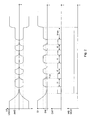
- Fig. 2 shows timing diagrams in a data transmission from a base station to the transponder of Fig. 1.
- the rectified voltage U1 is again shown as an envelope S1 as an envelope.
- the lower two diagrams show the field gap detection signal GAP and the transistor drive signals WD and MOD, respectively.
- the signals WD and MOD may have identical time courses.
- the base station Before the data transmission, the base station generates by its antenna coil, an alternating magnetic field with a frequency of 125kHz, which induces the AC voltage U1 between the input terminals A1 and A2 due to the inductive coupling.
- An amplitude of the alternating voltage U1 is limited or clamped by the voltage limiting unit BE to a maximum voltage UMAX.
- the base station To initiate the data transmission in the context of a write access to the transponder TR, the base station generates a field gap or a gap by suppression of the carrier signal.
- the voltage U1 of the parallel resonant circuit drops only slowly along the envelope, depending on its quality.
- the course of the rectified voltage U1 is evaluated in the signal processing unit SV.
- the signal processing unit SV When the voltage U1 falls below a threshold value SW for the first time, the signal processing unit SV generates an active signal GAP, i. the control unit SE indicates the detected field gap.
- the control unit SE then activates the signals MOD and WD, i. the transistor T1 is turned on or turned on.
- the through-connected transistor T1 causes an ohmic load in the form of the resistor R1 is connected between the input terminals A1 and A2, whereby the quality of the resonant circuit is reduced or increases its attenuation. This causes the envelope of the voltage U1 to decay significantly faster in the case of a field gap, i. subsequent field gaps can be detected with a much lower delay.
- the signal curve is shown in dashed lines with a lower attenuation, ie without a connected resistor R1.
- a time difference ⁇ t results between the conventional, undamped signal waveform and the more damped waveform of the invention.
- the signal curve according to the invention therefore corresponds much better to an ideal signal curve, in which the voltage U1 or the signal S1 suddenly decreases in the case of a field gap, as a result of which the field gap can be detected without delay.
- the resonant circuit damping is in this case essentially determined by the value of the resistor R1, i. the components caused by the antenna coil L1 and the capacitor C1 are negligible.
- the timing of the signal received by the transponder is therefore independent of the quality of the antenna coil L1 and the capacitor C1 after detection of the first field gap.
- the base station can generate its transmit signal timing independently of which antenna coil type is used in the transponder.
- the voltage limiting unit BE controlled by the active modulation signal MOD causes the voltage U1 to be limited or clamped to a value UWD.
- the voltage reduction of the voltage U1 to the maximum voltage value UWD also causes a faster detectability of a field gap, since the voltage U1 decreases from a lower initial value to the threshold value SW.
- the base station After the initiation of the data transmission by generating the first field gap, the base station switches on its carrier signal again. Due to the activated modulation signal MOD, the voltage limiting unit BE limits the voltage U1 to the value UWD.
- Characters sent by the base station following the initiation of the data transmission are coded by associated time durations t0 and t1, respectively, between time-consecutive field gaps. A first character value "0" is assigned the time duration t0 and a second character value "1" is assigned the time duration t1.
- the transmitted characters of the transponder TR determines the respective Time periods t0 and t1 between the field gaps and determined from the determined time duration, the value of the transmitted character. In the case shown, the exemplary binary string "1010" is transmitted to the transponder.
- the transponder TR recognizes the end of the data transmission. He then deactivates the signals WD and MOD. On the one hand, this causes an increase in the quality of the input resonant circuit and, on the other hand, an increase in the maximum value of the voltage U1 to the value UMAX, since the voltage limiting unit BE limits the voltage U1 to the maximum value UMAX due to the deactivated signal MOD.
- the threshold value SW instead of the threshold value SW, it is also possible to use a further, not shown, for example larger threshold value, in which case it is checked accordingly whether the voltage U1 for the maximum time period tmax is above this threshold value.
- the embodiments shown allow a high transmission range between base station and transponder due to the high usable quality of the input resonant circuits of antenna coil L1 and capacitor C1 and at the same time a substantially Q-independent timing of the signals generated by the base station.
Landscapes
- Engineering & Computer Science (AREA)
- Computer Networks & Wireless Communication (AREA)
- Computer Hardware Design (AREA)
- Microelectronics & Electronic Packaging (AREA)
- Physics & Mathematics (AREA)
- General Physics & Mathematics (AREA)
- Theoretical Computer Science (AREA)
- Near-Field Transmission Systems (AREA)
Applications Claiming Priority (1)
| Application Number | Priority Date | Filing Date | Title |
|---|---|---|---|
| DE200610007261 DE102006007261A1 (de) | 2006-02-10 | 2006-02-10 | Transponder und Verfahren zur drahtlosen Datenübertragung |
Publications (3)
| Publication Number | Publication Date |
|---|---|
| EP1818858A2 true EP1818858A2 (fr) | 2007-08-15 |
| EP1818858A3 EP1818858A3 (fr) | 2008-06-25 |
| EP1818858B1 EP1818858B1 (fr) | 2012-12-26 |
Family
ID=38057523
Family Applications (1)
| Application Number | Title | Priority Date | Filing Date |
|---|---|---|---|
| EP20070002809 Active EP1818858B1 (fr) | 2006-02-10 | 2007-02-09 | Transpondeur et procédé destiné à la transmission de données sans fil |
Country Status (3)
| Country | Link |
|---|---|
| US (2) | US20070194937A1 (fr) |
| EP (1) | EP1818858B1 (fr) |
| DE (1) | DE102006007261A1 (fr) |
Families Citing this family (8)
| Publication number | Priority date | Publication date | Assignee | Title |
|---|---|---|---|---|
| US7504935B2 (en) * | 2004-04-19 | 2009-03-17 | Siemens Aktiengesellschaft | Transponder |
| DE102007004814B4 (de) * | 2007-01-31 | 2013-06-06 | Continental Automotive Gmbh | Güteanpassung eines Empfangsschaltkreises |
| DE102007049560B4 (de) * | 2007-10-16 | 2013-07-11 | Texas Instruments Deutschland Gmbh | RFID-Transponder mit hoher Abwärtsdatengeschwindigkeit |
| DE102007049486B4 (de) | 2007-10-16 | 2018-08-09 | Texas Instruments Deutschland Gmbh | Hochleistungs-RFID-Transponder mit schneller Abwärtsverbindung |
| DE102010056031B4 (de) | 2010-12-27 | 2019-10-24 | Atmel Corp. | Passiver Transponder mit einer Ladeschaltung und Verfahren zur Erzeugung einer Versorgungsspannung für einen passiven Transponder |
| CN103842932A (zh) * | 2011-09-30 | 2014-06-04 | 英特尔公司 | 保持芯片上系统上的操作稳定性 |
| US9484629B2 (en) | 2011-11-22 | 2016-11-01 | Microsoft Technology Licensing, Llc | Multi-use antenna |
| CN110086508B (zh) * | 2019-03-28 | 2021-08-03 | 惠州Tcl移动通信有限公司 | 电压调整方法、系统、存储介质及移动终端 |
Citations (4)
| Publication number | Priority date | Publication date | Assignee | Title |
|---|---|---|---|---|
| EP0732663A2 (fr) | 1995-03-15 | 1996-09-18 | Omron Corporation | Support de données à taux de transmission de données élevé |
| EP0829940A2 (fr) | 1996-09-13 | 1998-03-18 | Hitachi, Ltd. | Système de transmission d'énergie, carte à puce et système de communication d'informations utilisant une carte à puce |
| DE19744782A1 (de) | 1997-10-10 | 1999-04-15 | Anatoli Stobbe | Verfahren und Vorrichtung zur Datenübertragung zwischen einem Schreib-Lesegerät und einem Transponder |
| WO2002009028A1 (fr) | 2000-07-21 | 2002-01-31 | Microcid Sa | Transpondeur passif a faible consommation |
Family Cites Families (15)
| Publication number | Priority date | Publication date | Assignee | Title |
|---|---|---|---|---|
| US5287112A (en) * | 1993-04-14 | 1994-02-15 | Texas Instruments Incorporated | High speed read/write AVI system |
| US5541604A (en) * | 1993-09-03 | 1996-07-30 | Texas Instruments Deutschland Gmbh | Transponders, Interrogators, systems and methods for elimination of interrogator synchronization requirement |
| GB9408588D0 (en) * | 1994-04-29 | 1994-06-22 | Disys Corp | Passive transponder |
| US6351215B2 (en) * | 1998-06-02 | 2002-02-26 | Rf Code, Inc. | Monitoring antenna system |
| US7180402B2 (en) * | 2000-06-06 | 2007-02-20 | Battelle Memorial Institute K1-53 | Phase modulation in RF tag |
| DE10245747B4 (de) * | 2002-10-01 | 2005-12-01 | Infineon Technologies Ag | Kontaktloser Datenträger |
| US7014112B2 (en) * | 2003-04-29 | 2006-03-21 | Hewlett-Packard Development Company, L.P. | Electronic identification label and interrogator for use therewith |
| JP3871667B2 (ja) * | 2003-08-18 | 2007-01-24 | 松下電器産業株式会社 | 非接触icカード |
| US7151455B2 (en) * | 2004-04-30 | 2006-12-19 | Kimberly-Clark Worldwide, Inc. | Activating a data tag by load or orientation or user control |
| DE102004031671B4 (de) * | 2004-06-30 | 2016-01-07 | Infineon Technologies Ag | Modulator-Schaltkreis, Sende-/Empfangs-Einrichtung,Lese-Vorrichtung und Verfahren zum Bilden eines modulierten Signals |
| DE102005032590A1 (de) * | 2004-07-12 | 2006-02-09 | Atmel Germany Gmbh | Modulator und Modulationsverfahren für eine Einrichtung zur drahtlosen Datenübertragung |
| JP4059874B2 (ja) * | 2004-09-30 | 2008-03-12 | 富士通株式会社 | 整流回路 |
| BRPI0617580B1 (pt) * | 2005-09-23 | 2022-09-27 | Ipico Innovation Inc | Transponder passivo, método de operar um transponder passivo |
| JP4766437B2 (ja) * | 2006-10-11 | 2011-09-07 | コヴィオ インコーポレイテッド | マルチモードタグとマルチモードタグの作製方法および使用方法 |
| DE102007049486B4 (de) * | 2007-10-16 | 2018-08-09 | Texas Instruments Deutschland Gmbh | Hochleistungs-RFID-Transponder mit schneller Abwärtsverbindung |
-
2006
- 2006-02-10 DE DE200610007261 patent/DE102006007261A1/de not_active Withdrawn
-
2007
- 2007-02-09 EP EP20070002809 patent/EP1818858B1/fr active Active
- 2007-02-12 US US11/705,009 patent/US20070194937A1/en not_active Abandoned
-
2011
- 2011-03-01 US US13/037,509 patent/US8847737B2/en active Active
Patent Citations (4)
| Publication number | Priority date | Publication date | Assignee | Title |
|---|---|---|---|---|
| EP0732663A2 (fr) | 1995-03-15 | 1996-09-18 | Omron Corporation | Support de données à taux de transmission de données élevé |
| EP0829940A2 (fr) | 1996-09-13 | 1998-03-18 | Hitachi, Ltd. | Système de transmission d'énergie, carte à puce et système de communication d'informations utilisant une carte à puce |
| DE19744782A1 (de) | 1997-10-10 | 1999-04-15 | Anatoli Stobbe | Verfahren und Vorrichtung zur Datenübertragung zwischen einem Schreib-Lesegerät und einem Transponder |
| WO2002009028A1 (fr) | 2000-07-21 | 2002-01-31 | Microcid Sa | Transpondeur passif a faible consommation |
Also Published As
| Publication number | Publication date |
|---|---|
| EP1818858B1 (fr) | 2012-12-26 |
| US8847737B2 (en) | 2014-09-30 |
| DE102006007261A1 (de) | 2007-08-23 |
| US20070194937A1 (en) | 2007-08-23 |
| EP1818858A3 (fr) | 2008-06-25 |
| US20110177781A1 (en) | 2011-07-21 |
Similar Documents
| Publication | Publication Date | Title |
|---|---|---|
| EP1818858B1 (fr) | Transpondeur et procédé destiné à la transmission de données sans fil | |
| EP0590122B1 (fr) | Procede et systeme de transmission de structures serielles de donnees pour systemes d'identification de supports d'information, ainsi que support d'information | |
| DE69532339T2 (de) | Kartenleser /-schreiber | |
| DE69831514T2 (de) | Identifizierungssystem | |
| EP2256662B1 (fr) | Procédé de détection de supports d'identification | |
| EP1508870A1 (fr) | Procédé pour le transfert des données sans fil entre une station de base et un transpondeur | |
| DE10301451A1 (de) | Verfahren sowie Sende- und Empfangseinrichtung zur drahtlosen Datenübertragung und Modulationseinrichtung | |
| DE102007034009B4 (de) | Datenübertragungsvorrichtung und -verfahren, die eine Kommunikation ohne eine Interferenz durch Umgebungsrauschen zulassen | |
| EP1675033B1 (fr) | Méthode de transmission de données sans fil | |
| EP3599573B1 (fr) | Procédé de transmission de données entre un appareil de lecture transpondeur radio et un transpondeur radio et transpondeur radio | |
| EP1587023A1 (fr) | Procédé de communication de données entre une station de base et un transpondeur | |
| DE102008040453B4 (de) | Vorrichtung zur berührungslosen Kommunikation und Verfahren zur berührungslosen Kommunikation | |
| EP1818853A2 (fr) | Procédé destiné à la transmission de données sans fil entre un poste de base et un transpondeur à l'aide d'un couplage inductif | |
| WO2008064824A1 (fr) | Procédé de transmission sans fil de données entre une station de base et un transpondeur passif, ainsi que transpondeur passif | |
| EP1836654B1 (fr) | Procede de localisation d'un transpondeur a base de retrodiffusion | |
| EP1586917A2 (fr) | Méthode pour faire un choix entre un ou plusieurs répondeurs | |
| EP2141637B1 (fr) | Support de données portatif doté d'une interface sans contact active et procédé de fonctionnement | |
| EP2474940B1 (fr) | unité transpondeur | |
| DE102005009765B3 (de) | Selektionsverfahren für eine Datenkommunikation zwischen Basisstation und Transponder | |
| EP1147487B1 (fr) | Procede de transmission de donnees sans contact et transpondeur pour un systeme de transmission de donnees sans contact | |
| DE19827476C1 (de) | Verfahren zum bidirektionalen Übertragen digitaler Daten | |
| EP1587022B1 (fr) | Méthode de transmission de données sans fil | |
| DE102004018556A1 (de) | Verfahren zur Datenkommunikation zwischen einer Basisstation und einem Transponder | |
| EP1808968B1 (fr) | Procédé de fonctionnement d'un transpondeur et transpondeur | |
| DE69727034T2 (de) | Transpondersystem |
Legal Events
| Date | Code | Title | Description |
|---|---|---|---|
| PUAI | Public reference made under article 153(3) epc to a published international application that has entered the european phase |
Free format text: ORIGINAL CODE: 0009012 |
|
| AK | Designated contracting states |
Kind code of ref document: A2 Designated state(s): AT BE BG CH CY CZ DE DK EE ES FI FR GB GR HU IE IS IT LI LT LU LV MC NL PL PT RO SE SI SK TR |
|
| AX | Request for extension of the european patent |
Extension state: AL BA HR MK YU |
|
| RIN1 | Information on inventor provided before grant (corrected) |
Inventor name: KURZ, ALEXANDER Inventor name: BERHORST, MARTIN Inventor name: SCHNEIDER, PETER |
|
| PUAL | Search report despatched |
Free format text: ORIGINAL CODE: 0009013 |
|
| AK | Designated contracting states |
Kind code of ref document: A3 Designated state(s): AT BE BG CH CY CZ DE DK EE ES FI FR GB GR HU IE IS IT LI LT LU LV MC NL PL PT RO SE SI SK TR |
|
| AX | Request for extension of the european patent |
Extension state: AL BA HR MK RS |
|
| 17P | Request for examination filed |
Effective date: 20080715 |
|
| 17Q | First examination report despatched |
Effective date: 20080818 |
|
| AKX | Designation fees paid |
Designated state(s): DE FR |
|
| RAP1 | Party data changed (applicant data changed or rights of an application transferred) |
Owner name: ATMEL AUTOMOTIVE GMBH |
|
| GRAP | Despatch of communication of intention to grant a patent |
Free format text: ORIGINAL CODE: EPIDOSNIGR1 |
|
| GRAS | Grant fee paid |
Free format text: ORIGINAL CODE: EPIDOSNIGR3 |
|
| GRAA | (expected) grant |
Free format text: ORIGINAL CODE: 0009210 |
|
| AK | Designated contracting states |
Kind code of ref document: B1 Designated state(s): DE FR |
|
| REG | Reference to a national code |
Ref country code: DE Ref legal event code: R096 Ref document number: 502007011091 Country of ref document: DE Effective date: 20130307 |
|
| REG | Reference to a national code |
Ref country code: DE Ref legal event code: R082 Ref document number: 502007011091 Country of ref document: DE Representative=s name: GRUENECKER, KINKELDEY, STOCKMAIR & SCHWANHAEUS, DE |
|
| REG | Reference to a national code |
Ref country code: DE Ref legal event code: R081 Ref document number: 502007011091 Country of ref document: DE Owner name: ATMEL CORPORATION, US Free format text: FORMER OWNER: ATMEL GERMANY GMBH, 74072 HEILBRONN, DE Effective date: 20130103 Ref country code: DE Ref legal event code: R082 Ref document number: 502007011091 Country of ref document: DE Representative=s name: GRUENECKER, KINKELDEY, STOCKMAIR & SCHWANHAEUS, DE Effective date: 20130515 Ref country code: DE Ref legal event code: R081 Ref document number: 502007011091 Country of ref document: DE Owner name: ATMEL CORPORATION, US Free format text: FORMER OWNER: ATMEL AUTOMOTIVE GMBH, 74072 HEILBRONN, DE Effective date: 20130515 Ref country code: DE Ref legal event code: R081 Ref document number: 502007011091 Country of ref document: DE Owner name: ATMEL CORPORATION, SAN JOSE, US Free format text: FORMER OWNER: ATMEL GERMANY GMBH, 74072 HEILBRONN, DE Effective date: 20130103 Ref country code: DE Ref legal event code: R081 Ref document number: 502007011091 Country of ref document: DE Owner name: ATMEL CORPORATION, SAN JOSE, US Free format text: FORMER OWNER: ATMEL AUTOMOTIVE GMBH, 74072 HEILBRONN, DE Effective date: 20130515 Ref country code: DE Ref legal event code: R082 Ref document number: 502007011091 Country of ref document: DE Representative=s name: GRUENECKER PATENT- UND RECHTSANWAELTE PARTG MB, DE Effective date: 20130515 |
|
| PLBE | No opposition filed within time limit |
Free format text: ORIGINAL CODE: 0009261 |
|
| STAA | Information on the status of an ep patent application or granted ep patent |
Free format text: STATUS: NO OPPOSITION FILED WITHIN TIME LIMIT |
|
| REG | Reference to a national code |
Ref country code: FR Ref legal event code: ST Effective date: 20131031 |
|
| 26N | No opposition filed |
Effective date: 20130927 |
|
| REG | Reference to a national code |
Ref country code: DE Ref legal event code: R097 Ref document number: 502007011091 Country of ref document: DE Effective date: 20130927 |
|
| PG25 | Lapsed in a contracting state [announced via postgrant information from national office to epo] |
Ref country code: FR Free format text: LAPSE BECAUSE OF NON-PAYMENT OF DUE FEES Effective date: 20130228 |
|
| P01 | Opt-out of the competence of the unified patent court (upc) registered |
Effective date: 20230528 |
|
| PGFP | Annual fee paid to national office [announced via postgrant information from national office to epo] |
Ref country code: DE Payment date: 20260121 Year of fee payment: 20 |