EP1819042A2 - Verkapselung auf Waferebene für eine Oberflächenschallwellenvorrichtung und Herstellungsverfahren dafür - Google Patents
Verkapselung auf Waferebene für eine Oberflächenschallwellenvorrichtung und Herstellungsverfahren dafür Download PDFInfo
- Publication number
- EP1819042A2 EP1819042A2 EP07101051A EP07101051A EP1819042A2 EP 1819042 A2 EP1819042 A2 EP 1819042A2 EP 07101051 A EP07101051 A EP 07101051A EP 07101051 A EP07101051 A EP 07101051A EP 1819042 A2 EP1819042 A2 EP 1819042A2
- Authority
- EP
- European Patent Office
- Prior art keywords
- cap
- wafer
- via portion
- top surface
- cap wafer
- Prior art date
- Legal status (The legal status is an assumption and is not a legal conclusion. Google has not performed a legal analysis and makes no representation as to the accuracy of the status listed.)
- Withdrawn
Links
Images


Classifications
-
- H—ELECTRICITY
- H03—ELECTRONIC CIRCUITRY
- H03H—IMPEDANCE NETWORKS, e.g. RESONANT CIRCUITS; RESONATORS
- H03H9/00—Networks comprising electromechanical or electro-acoustic elements; Electromechanical resonators
- H03H9/02—Details
- H03H9/05—Holders or supports
- H03H9/10—Mounting in enclosures
- H03H9/1064—Mounting in enclosures for surface acoustic wave [SAW] devices
- H03H9/1092—Mounting in enclosures for surface acoustic wave [SAW] devices the enclosure being defined by a cover cap mounted on an element forming part of the surface acoustic wave [SAW] device on the side of the IDT's
-
- B—PERFORMING OPERATIONS; TRANSPORTING
- B43—WRITING OR DRAWING IMPLEMENTS; BUREAU ACCESSORIES
- B43K—IMPLEMENTS FOR WRITING OR DRAWING
- B43K23/00—Holders or connectors for writing implements; Means for protecting the writing-points
- B43K23/012—Holders for attachment to finger tips
-
- B—PERFORMING OPERATIONS; TRANSPORTING
- B43—WRITING OR DRAWING IMPLEMENTS; BUREAU ACCESSORIES
- B43K—IMPLEMENTS FOR WRITING OR DRAWING
- B43K23/00—Holders or connectors for writing implements; Means for protecting the writing-points
- B43K23/08—Protecting means, e.g. caps
- B43K23/12—Protecting means, e.g. caps for pens
-
- B—PERFORMING OPERATIONS; TRANSPORTING
- B43—WRITING OR DRAWING IMPLEMENTS; BUREAU ACCESSORIES
- B43K—IMPLEMENTS FOR WRITING OR DRAWING
- B43K24/00—Mechanisms for selecting, projecting, retracting or locking writing units
- B43K24/02—Mechanisms for selecting, projecting, retracting or locking writing units for locking a single writing unit in only fully projected or retracted positions
-
- H—ELECTRICITY
- H10—SEMICONDUCTOR DEVICES; ELECTRIC SOLID-STATE DEVICES NOT OTHERWISE PROVIDED FOR
- H10W—GENERIC PACKAGES, INTERCONNECTIONS, CONNECTORS OR OTHER CONSTRUCTIONAL DETAILS OF DEVICES COVERED BY CLASS H10
- H10W20/00—Interconnections in chips, wafers or substrates
- H10W20/01—Manufacture or treatment
- H10W20/021—Manufacture or treatment of interconnections within wafers or substrates
- H10W20/023—Manufacture or treatment of interconnections within wafers or substrates the interconnections being through-semiconductor vias
- H10W20/0242—Manufacture or treatment of interconnections within wafers or substrates the interconnections being through-semiconductor vias comprising etching via holes from the back sides of the chips, wafers or substrates
-
- H—ELECTRICITY
- H10—SEMICONDUCTOR DEVICES; ELECTRIC SOLID-STATE DEVICES NOT OTHERWISE PROVIDED FOR
- H10W—GENERIC PACKAGES, INTERCONNECTIONS, CONNECTORS OR OTHER CONSTRUCTIONAL DETAILS OF DEVICES COVERED BY CLASS H10
- H10W20/00—Interconnections in chips, wafers or substrates
- H10W20/01—Manufacture or treatment
- H10W20/021—Manufacture or treatment of interconnections within wafers or substrates
- H10W20/023—Manufacture or treatment of interconnections within wafers or substrates the interconnections being through-semiconductor vias
- H10W20/0245—Manufacture or treatment of interconnections within wafers or substrates the interconnections being through-semiconductor vias comprising use of blind vias during the manufacture
-
- H—ELECTRICITY
- H10—SEMICONDUCTOR DEVICES; ELECTRIC SOLID-STATE DEVICES NOT OTHERWISE PROVIDED FOR
- H10W—GENERIC PACKAGES, INTERCONNECTIONS, CONNECTORS OR OTHER CONSTRUCTIONAL DETAILS OF DEVICES COVERED BY CLASS H10
- H10W20/00—Interconnections in chips, wafers or substrates
- H10W20/20—Interconnections within wafers or substrates, e.g. through-silicon vias [TSV]
- H10W20/211—Through-semiconductor vias, e.g. TSVs
- H10W20/212—Top-view shapes or dispositions, e.g. top-view layouts of the vias
- H10W20/2125—Top-view shapes
-
- H—ELECTRICITY
- H10—SEMICONDUCTOR DEVICES; ELECTRIC SOLID-STATE DEVICES NOT OTHERWISE PROVIDED FOR
- H10W—GENERIC PACKAGES, INTERCONNECTIONS, CONNECTORS OR OTHER CONSTRUCTIONAL DETAILS OF DEVICES COVERED BY CLASS H10
- H10W90/00—Package configurations
- H10W90/701—Package configurations characterised by the relative positions of pads or connectors relative to package parts
- H10W90/751—Package configurations characterised by the relative positions of pads or connectors relative to package parts of bond wires
- H10W90/754—Package configurations characterised by the relative positions of pads or connectors relative to package parts of bond wires between a chip and a stacked insulating package substrate, interposer or RDL
Definitions
- the present invention relates to a surface acoustic wave device wafer level package that packages a surface acoustic wave device according to a wafer level packaging method, and a fabrication method thereof.
- a surface acoustic wave (SAW) device is generally used as an electronic part such as a filter, a delay line, or an oscillator of an electronic device transmitting and receiving waves, and is also employed as a radio frequency (RF) part in a mobile phone to suppress unnecessary signals.
- SAW surface acoustic wave
- RF radio frequency
- the SAW filter 10 comprises a ceramics package 11, a cavity 12 formed to be hollow in the package 11, a metal cap 13 to hermitically seal an opening of the cavity 12, and a SAW element 14 packed in the cavity 12.
- the package 11 forms a three layer structure in which three substrates 11a, 11b, and 11c are bonded.
- An electrode pad 15, a wire pattern 16, and a foot pattern 17 are formed over the substrates 11a, 11b, and 11c.
- the SAW element 14 is fixed on a bottom portion of the cavity 12 such that a surface with an interdigital transducer (IDT) faces up.
- the SAW device 14 is electrically connected with the wire pattern 15, which is exposed to an inside of the cavity 12, by a metal wire 18.
- the metal cap 13 is deposited onto a top surface of the package 11 by binding material 19 such as solder or resin.
- the SAW filter 10 with the above configuration has the SAW element 14 that is electrically connected with the package 11 through a wire so as to hermitically seal the SAW element, and the metal cap 13 is deposited onto the top surface of the package 11 so that there is a limit of how compact the SAW filter 10 can be made. As a size of the SAW element 14 gets smaller, manufacturing of the SAW filter 10 becomes more complicated so that the manufacturing cost can increase.
- a surface acoustic wave (SAW) device wafer level package including a SAW device in which a SAW element is formed on a top surface of a device wafer, a cap wafer which is bonded with a top surface of the SAW device and has a viahole penetrating the cap wafer, a conductive member to fill a part of the viahole, wherein the viahole has a first via portion and a second via portion, the first via portion has a gradually smaller diameter from a bottom surface of the cap wafer until a certain depth, and the second via portion has a gradually greater diameter from the first via portion until a top surface of the cap wafer.
- SAW surface acoustic wave
- the present invention has been conceived to solve the above-mentioned problems occurring in the prior art.
- the invention thus provides a SAW device wafer level package having an improved structure so as to be miniaturized.
- the SAW device may further include a device pad formed on the top surface of the device wafer to connect with the SAW element, and a device sealing line formed on the top surface of the device wafer.
- the SAW device wafer level package may further include a cap pad formed on the top surface of the cap wafer, and a connection pad formed on the bottom surface of the cap wafer to electrically connect with the cap pad through the conductive member.
- the conductive member may include a first metal layer, which is formed to cover insides of the first via portion and the second via portion, and a lower end of which is electrically connected with the connection pad, and a second metal layer, which is formed on the first metal layer to fill the second via portion, to be electrically connected with the cap pad.
- the second metal layer may be formed by electroplating an upper portion of the first metal layer.
- the cap pad may be formed to cover an upper portion of the viahole.
- connection pad may be connected with the conductive member at a boundary between the viahole and the bottom surface of the cap wafer.
- the SAW device wafer level package may further include a sealing line formed on a bottom surface of the cap wafer to be extended from a boundary between the viahole and the bottom surface of the cap wafer.
- the SAW device wafer level package may further include a cavity formed between the cap wafer and the SAW device to receive the SAW element.
- the cap wafer may be formed of LiTaO 3 or LiNbO 3 .
- the SAW device may be formed of the same material as the cap wafer.
- the first via portion may be formed to have a deeper depth than the second via portion.
- the invention also provides a SAW device wafer level packaging method, including operations of a) forming a SAW device in which a SAW element is formed on a top surface of a device wafer, b) forming a cap wafer in which a conductive member fills a part of the viahole that has a first via portion and a second via portion, the first via portion has a gradually smaller diameter from a bottom surface of the cap wafer until a certain depth, and the second via portion has a gradually greater diameter from the first via portion until a top surface of the cap wafer, c) bonding the packaging cap with a top surface of the SAW device.
- the operation b) may include operations of b1) etching the bottom surface of the cap wafer by a certain depth to form the first via portion, b2) etching the top surface of the cap wafer by a certain depth to the second via portion to connect with the first via portion, and b3) filling the first via portion and the second via portion with metal materials of each different amount ratio to form the conductive member.
- the operation b) may include operations of b4) forming the cap pad on the top surface of the cap wafer to electrically connect with the conductive member, and b5) forming a connection pad, which electrically connects with the conductive member, and a cap sealing line, which is short-circuited with the conductive member, on the bottom surface of the cap wafer.
- the operations b1) and b2) may form the first via portion and the second via portion to have each different depth.
- the forming of the first via portion may include operations of patterning a dry film resist on the bottom surface of the cap wafer, and sandblasting the bottom surface of the cap wafer, which is exposed by the dry film resist.
- the forming of the second via portion may include operations of patterning a dry film resist on the top surface of the cap wafer, and sandblasting the top surface of the cap wafer, which is exposed by the dry film resist.
- the operation b3) may include operations of depositing a first metal layer to cover a surface of the cap wafer including the viahole, electroplating a metal material on the first metal layer to fill the second via portion, and grinding the top surface and the bottom surface of the cap wafer to be exposed and removing the first metal layer from the top surface and the bottom surface of the cap wafer.
- the operation b4) may pattern and form the cap pad so as to be disposed above the viahole and cover the conductive member.
- the operation b5) may include a first operation forming a metal material by a certain depth to cover the bottom surface of the cap wafer, and a second operation etching the metal material according to a certain pattern using a photo resist to simultaneously form the connection pad and the cap sealing line.
- the second operation may include operations of partially removing the conductive member in the viahole so that a part of the viahole is exposed and the conductive member can be short-circuited with the cap sealing line.
- the operation b5) may include a first operation forming a metal material by a certain thickness to cover the bottom surface of the cap wafer, and a second operation etching the metal material according to a certain pattern using a photo resist to simultaneously form the connection pad and the cap sealing line, and partially removing the first metal layer in the viahole for the cap sealing line to be short-circuited with the first metal layer.
- the operation a) may include an operation of forming a device pad and a device sealing line on the top surface of the device wafer.
- the operation c) may be performed by bonding a cap sealing line, which is formed on a bottom surface of the cap wafer, with a device sealing line, which is formed on a top surface of the device wafer.
- the cap wafer may be formed of LiTaO 3 or LiNbO 3 .
- the device wafer may be formed of the same material as the cap wafer.
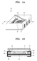
- a surface acoustic wafer (SAW) device wafer level package 100 comprises a SAW device 110 in which a SAW element 112 is formed on a top surface of a device wafer 111, and a packaging cap 120 bonded with a top surface of the SAW device 110.
- the packaging cap 120 is bonded with the SAW device 110 so that a cavity 130, which is formed between the packaging cap 120 and the SAW device 110, receives the SAW element 112.
- the SAW device 110 comprises the device wafer 111 formed of piezoelectric material such as LiTaO 3 or LiNbO 3 , the SAW element 112 formed on a top surface of the device wafer 111, a device pad 113 formed on a top surface of the device wafer 111 according to a predetermined pattern, and a device sealing line 114.
- the SAW element 112 may be formed on a bottom portion of the cavity 130, that is, on a top surface of the device wafer 111 for a surface with an InterDigital transducer to face up.
- the SAW element 112 may be formed by depositing metal material on the device wafer 111 according to a predetermined pattern.
- the device pad 113 and the device sealing line 114 are formed to have the same height as each other.
- the device pad 113 and the device sealing line 114 may be formed of the same metal material.
- the SAW element 112, the device pad 113, and the device sealing line 114 may be mainly formed of Au, Al, Cu, Ti, Cr, Ta, and Ni.
- the device pad 113 is provided in a plurality.
- the device sealing line 114 is to bond the SAW device 110 with the packaging cap 120 for packaging.
- the packaging cap 120 comprises a cap wafer 121 with a viahole H, a cap pad 122 formed on a top surface of the cap wafer 121, a connection pad 123 formed on a bottom surface of the cap wafer 121, and a cap sealing line 124.
- the cap wafer 121 may be formed of the same material as the device wafer 111.
- the viahole H upwardly and downwardly penetrates the cap wafer 121.
- the viahole H comprises a first via portion H1 formed to a certain depth from a bottom surface of the cap wafer 121, and a second via portion H2 formed to a certain depth from a top surface of the cap wafer 121.
- the first via portion H1 and the second via portion H2 are each formed to have a gradually smaller diameter from the outside surface of the cap wafer 121 towards the center of the cap wafer 121, and are connected to each other.
- the top surface and the bottom surface of the cap wafer 121 are etched according to separate processes so that the viahole H is divided into the first via portion H1 and the second via portion H2.
- first via portion H1 and the second via portion H2 are formed to have different depths.
- the second via portion H2 which will be fully filled with a conductive member 125, is formed to have a smaller depth than the first via portion H2.
- the viahole H is filled with the conductive member 125.
- the conductive member 125 which will be in detail explained below, is formed by depositing a metal material to form a seed layer and electroplating a metal material on the seed layer, which is a metal layer, to fill the viahole H.
- the conductive member 125 entirely fills the second via portion H2 to connect with the cap pad 122, and is sprayed by a predetermined thickness over a part of an inside of the first via portion H1. Accordingly, an upper portion of the conductive member 125 is connected with the cap pad 122, and a lower portion of the conductive member 125 is connected with the connection pad 123 so as to electrically connect the cap pad 122 and the connection pad 123.
- the conductive member 125 is not electrically connected with the cap sealing line 124.
- Cap pads 122 are formed on a direct top surface of the cap wafer 121 to correspond to each viahole H, and preferably, but not necessarily, they are formed according to a certain pattern to cover the conductive member 125 formed in the viahole H.
- the cap pads 122 are formed by patterning a metal material on the top surface of the cap wafer 121.
- connection pads 123 there are a plurality of connection pads 123 to correspond to the number of the device pads 113.
- the connection pads 123 are bonded with the device pads 113 to be electrically connected.
- the cap sealing line 124 is formed of the same material as the connection pad 123, and may be formed simultaneously with the connection pad 123.
- the cap sealing line 124 is formed to correspond to the device sealing line 114. Accordingly, while bonding the connection pads 123 with the device pads 113, bonding the device sealing line 114 with the cap sealing line 124 makes the cavity 130 airtight.
- connection pad 123 is extended according to a certain pattern from a boundary between the viahole H and a bottom surface of the cap wafer 121 so as to be connected with the conductive member 125.
- the cap sealing line 124 is extended according to a certain pattern from a boundary between the viahole H and a bottom surface of the cap wafer 121 so as to come into contact with an exposed surface S1 of the viahole H. Accordingly, the cap sealing line 124 can be short-circuited with the conductive member 125.
- the cap pads 122 are formed on each top portion of the viahole H so that intervals between the cap pads 122 can be narrow and a size of the packaging cap 120 can be reduced.
- connection pads 123 and the cap sealing lines 124 are formed to come into contact with the viahole H. Accordingly, a distance between the cap sealing lines 124 formed at opposite side of the packaging cap 120 can be shortened so that the left and right size of the packaging cap 120 in the drawing can be reduced.
- the viahole H is divided into up and down, that is, the first via portion H1 and the second via portion H2 so that the diameter of the viahole H can be minimally formed.
- the diameter of the viahole H is minimized, and accordingly, a high degree of freedom in designing various patterns can be provided so that the interval between the cap sealing lines 124 can be reduced.
- reference numeral 140 denotes a solder ball formed on the cap pads 122.
- the solder ball 140 is for mounting the completed SAW device wafer level package onto a printed circuit board (PCB) substrate.
- PCB printed circuit board
- a dry film resist (DFR) 210 is patterned on a bottom surface of the cap wafer 121 and the bottom surface of the cap wafer 121, which is exposed through the dry film resist 210, is etched by a certain depth to form the first via portion H1 as shown in FIG. 3A.
- the first via portion H1 may be formed according to a sand blasting so that it has a gradually narrower diameter as further from the bottom surface of the cap wafer 121.
- a dry film resist 220 is patterned on the top surface of the cap wafer 121 and the top surface of the cap wafer 121, which is exposed through the dry film resist 220, is etched to form the second via portion H2.
- the second via portion H2 may be formed also by sand blasting.
- the second via portion H2 is formed with such a depth so as to connect with the first via portion H1.
- the bottom surface and the top surface of the cap wafer 121 are etched according to two steps to form the viaholes H so that the diameter of the viahole H is prevented from unnecessarily enlarging and accordingly, the viahole H can be formed in a small size.
- the second via portion H2 is formed to have a lower depth than the first via portion H1.
- the first via portion H1 which is earlier formed, may be formed to have a sufficiently long depth.
- the second via portion H2 is formed also to have a gradually narrower diameter as it gets further from the top surface of the cap wafer 121.
- a seed layer 230 is formed to a certain thickness on an exposed surface of the cap wafer 121.
- the seed layer 230 may be formed by depositing a metal material.
- the seed layer 230 is formed to cover all the inside of the viahole H including the top surface and bottom surface of the cap wafer 121.
- the seed layer 230 may be formed of a metal mainly comprising Cr, Au, and Cu.
- the first via portion H2 is filled so that the conductive member 125 can be formed as explained with reference to FIG. 2.
- the viahole H is electroplated on the top surface of the cap wafer 121, the metal material fills only the second via portion H2, but passes the first via portion H1 as unfilled, because the diameter of the boundary between the second via portion H2 and the first via portion H1 becomes the narrowest. Accordingly, only the seed layer 230, which is previously deposited, is left on the first via portion H1.
- the viahole H is divided into the first via portion H1 and the second via portion H2 so that the viahole H can be partially electroplated and filled.
- the earlier-deposited seed layer 230 is referred to as a first metal layer and the later-deposited seed layer 230 is referred to as a second metal layer.
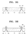
- the top surface and the bottom surface of the cap wafer 121 each are ground and planarized as shown in FIG. 3E.
- the planarizing for example, a grinding and a polishing, removes the seed layer 230 formed on the top surface and the bottom surface of the cap wafer 121.
- the cap pads 122 are formed on the top surface of the cap wafer 121.
- the cap pad 122 may be formed by spraying a metal material on the top surface of the cap wafer 121 and pattering a mask.
- the cap pad 122 is formed to cover a direct top portion, that is, the conductive member 125, of the viahole H.
- connection pad 123 and the cap sealing line 124 are formed on the bottom surface of the cap wafer 121.
- the connection pad 123 is extended from the boundary between the viahole H and the bottom surface of the cap wafer 121 so as to be electrically connected with the conductive member 125.
- the cap sealing line 124 comes into contact with the exposed surface S1, from which the conductive member 125 is removed, so as to be short-circuited with the conductive member 125.
- the connection pad 123 and the cap sealing line 124 may be simultaneously formed of the same metal material, and have the same height as each other.
- the exposed surface S1 is formed as following process: the metal material is formed on the bottom surface of the cap wafer 121, the metal material is patterned using a photo resist to form the connection pad 123 and the cap sealing line 124; at this time, a part of the conductive member 125 is together patterned so that the exposed surface S1 can be formed.
- connection pad 123 and the cap sealing line 124 may be formed according to a lift off.
- connection pad 123 and the cap sealing line 124 can be formed around the viahole H. Accordingly, the interval between the connection pads 123, which are disposed at the right and left sides in the drawings, can be reduced. In other words, if the connection pads are formed on a direct bottom portion of the viahole H, the interval between the connection pads is spaced apart so that the size of the cap wafer 121 becomes great. Additionally, since the cap sealing line 124 can also be formed adjacent to the viahole H, a high degree of freedom in the designing is provided so that the size of the cap wafer 121 can be reduced.
- the connection pad 123 and the cap sealing line 124 may be formed of Au, Cu, or Al.
- the solder ball 140 may be formed on the top portion of the cap pad 122.
- the solder ball 140 may be formed also after the cap wafer 121 is packaged with the SAW device 110.
- the packaging cap 120 is bonded with the SAW device 110, which is fabricated according to another separate process so that the SAW device wafer level package is completed.
- the SAW device 110 can be simply fabricated by patterning and forming the SAW element 112, the device pad 113, and the device sealing line 114 on the device wafer 111.
- connection pad 123 is bonded with the device pad 113 and the cap sealing line 124 is bonded with the device sealing line 114. Then, the cavity 130 receiving the SAW element 112 is hermitically sealed, and the SAW device 112 can be connected with exterior electronic devices through the device pad 113, the connection pad 123, the conductive member 125 and the cap pad 122.
- the SAW device wafer level package and fabrication method thereof according to exemplary embodiments of the present invention are applied, the SAW device wafer and the packaging cap are fabricated according to separate processes and then packaged. Accordingly, a simplified and miniaturized SAW device wafer level package can be provided.
- the viahole is formed according the first process and the second process on the cap wafer of the packaging cap so that the size of the viahole can be reduced.
- the viahole is formed to have each different depth on the top surface and the bottom surface of the cap wafer such that it can be divided into the first via portion and the second via portion. Accordingly, when filled by electroplating, the viahole can be partially filled. Therefore, the seed layer of the unfilled first via portion can be easily fabricated in the following processes. Furthermore, electrical characteristic of the conductive member by the electroplating can be improved.
- the size of the viahole is reduced so that the degree of freedom in designing the forming location of the cap pad and the connection pad, which are electrically connected through the viahole, can increase. Accordingly, the size of the package can be reduced.
Landscapes
- Physics & Mathematics (AREA)
- Acoustics & Sound (AREA)
- Surface Acoustic Wave Elements And Circuit Networks Thereof (AREA)
Applications Claiming Priority (1)
| Application Number | Priority Date | Filing Date | Title |
|---|---|---|---|
| KR1020060009779A KR100731351B1 (ko) | 2006-02-01 | 2006-02-01 | 탄성 표면파 디바이스 웨이퍼 레벨 패키지 및 그 패키징방법 |
Publications (2)
| Publication Number | Publication Date |
|---|---|
| EP1819042A2 true EP1819042A2 (de) | 2007-08-15 |
| EP1819042A3 EP1819042A3 (de) | 2008-01-23 |
Family
ID=37989046
Family Applications (1)
| Application Number | Title | Priority Date | Filing Date |
|---|---|---|---|
| EP07101051A Withdrawn EP1819042A3 (de) | 2006-02-01 | 2007-01-23 | Verkapselung auf Waferebene für eine Oberflächenschallwellenvorrichtung und Herstellungsverfahren dafür |
Country Status (4)
| Country | Link |
|---|---|
| US (1) | US7545017B2 (de) |
| EP (1) | EP1819042A3 (de) |
| JP (1) | JP2007208968A (de) |
| KR (1) | KR100731351B1 (de) |
Cited By (3)
| Publication number | Priority date | Publication date | Assignee | Title |
|---|---|---|---|---|
| CN107251661A (zh) * | 2015-02-23 | 2017-10-13 | 凸版印刷株式会社 | 印刷配线板及其制造方法 |
| CN108666410A (zh) * | 2017-03-28 | 2018-10-16 | 天津威盛电子有限公司 | 表面声波晶片级封装及其所用的pcb的制造方法 |
| CN109088613A (zh) * | 2018-06-28 | 2018-12-25 | 深圳华远微电科技有限公司 | 声表面波滤波器及其封装方法和电子设备 |
Families Citing this family (15)
| Publication number | Priority date | Publication date | Assignee | Title |
|---|---|---|---|---|
| KR100750741B1 (ko) * | 2006-09-15 | 2007-08-22 | 삼성전기주식회사 | 캡 웨이퍼, 이를 구비한 반도체 칩, 및 그 제조방법 |
| US7696064B2 (en) * | 2007-10-11 | 2010-04-13 | Skyworks Solutions, Inc. | Methods for forming a through via |
| WO2009048861A2 (en) * | 2007-10-11 | 2009-04-16 | Skyworks Solutions, Inc. | Methods for forming a through via |
| JP5056837B2 (ja) * | 2009-12-21 | 2012-10-24 | 株式会社村田製作所 | 圧電デバイスの製造方法 |
| US9048809B2 (en) * | 2012-01-03 | 2015-06-02 | International Business Machines Corporation | Method of manufacturing switchable filters |
| JP2015106655A (ja) * | 2013-11-29 | 2015-06-08 | 富士通株式会社 | 積層基板製造方法及び積層基板 |
| US20150279793A1 (en) * | 2014-03-27 | 2015-10-01 | Taiwan Semiconductor Manufacturing Company Ltd. | Semiconductor structure and manufacturing method thereof |
| CN104445046B (zh) * | 2014-06-24 | 2016-05-18 | 华天科技(昆山)电子有限公司 | 新型晶圆级mems芯片封装结构及其封装方法 |
| KR102588790B1 (ko) | 2016-02-04 | 2023-10-13 | 삼성전기주식회사 | 음향파 필터 장치, 음향파 필터 장치 제조용 패키지 |
| US10629468B2 (en) | 2016-02-11 | 2020-04-21 | Skyworks Solutions, Inc. | Device packaging using a recyclable carrier substrate |
| US10453763B2 (en) | 2016-08-10 | 2019-10-22 | Skyworks Solutions, Inc. | Packaging structures with improved adhesion and strength |
| CN108313974A (zh) * | 2018-02-07 | 2018-07-24 | 宜确半导体(苏州)有限公司 | 声学设备及其晶圆级封装方法 |
| US11581870B2 (en) | 2019-09-27 | 2023-02-14 | Skyworks Solutions, Inc. | Stacked acoustic wave resonator package with laser-drilled VIAS |
| US12562711B2 (en) * | 2021-07-15 | 2026-02-24 | Skyworks Solutions, Inc. | Wafer level package having enhanced thermal dissipation |
| US12581979B2 (en) * | 2022-03-31 | 2026-03-17 | Beijing Boe Optoelectronics Technology Co., Ltd. | Substrate and preparation method thereof, integrated passive device, and electronic apparatus |
Citations (5)
| Publication number | Priority date | Publication date | Assignee | Title |
|---|---|---|---|---|
| JPH08213874A (ja) | 1995-02-03 | 1996-08-20 | Matsushita Electric Ind Co Ltd | 表面弾性波装置及びその製造方法 |
| US6400172B1 (en) | 1997-12-18 | 2002-06-04 | Micron Technology, Inc. | Semiconductor components having lasered machined conductive vias |
| US20040104791A1 (en) | 2002-08-13 | 2004-06-03 | Yoshio Satoh | Acoustic wave device and method of producing the same |
| EP1432123A2 (de) | 2002-12-19 | 2004-06-23 | Murata Manufacturing Co., Ltd. | Elektronisches Bauteil und dessen Herstellungsverfahren |
| US20040232802A1 (en) | 2002-07-31 | 2004-11-25 | Yoshihiro Koshido | Piezoelectric component and method for manufacturing the same |
Family Cites Families (6)
| Publication number | Priority date | Publication date | Assignee | Title |
|---|---|---|---|---|
| US3648131A (en) * | 1969-11-07 | 1972-03-07 | Ibm | Hourglass-shaped conductive connection through semiconductor structures |
| US20020004320A1 (en) * | 1995-05-26 | 2002-01-10 | David V. Pedersen | Attaratus for socketably receiving interconnection elements of an electronic component |
| US6867493B2 (en) * | 2000-11-15 | 2005-03-15 | Skyworks Solutions, Inc. | Structure and method for fabrication of a leadless multi-die carrier |
| AU2003233704A1 (en) * | 2002-05-31 | 2003-12-19 | Spectalis Corp. | Electro-optic modulators |
| KR100541087B1 (ko) * | 2003-10-01 | 2006-01-10 | 삼성전기주식회사 | 마이크로 디바이스를 위한 웨이퍼 레벨 패키지 및 제조방법 |
| JP4210958B2 (ja) * | 2004-07-14 | 2009-01-21 | 株式会社村田製作所 | 圧電デバイス |
-
2006
- 2006-02-01 KR KR1020060009779A patent/KR100731351B1/ko not_active Expired - Lifetime
- 2006-06-07 US US11/447,969 patent/US7545017B2/en active Active
-
2007
- 2007-01-05 JP JP2007000825A patent/JP2007208968A/ja not_active Withdrawn
- 2007-01-23 EP EP07101051A patent/EP1819042A3/de not_active Withdrawn
Patent Citations (5)
| Publication number | Priority date | Publication date | Assignee | Title |
|---|---|---|---|---|
| JPH08213874A (ja) | 1995-02-03 | 1996-08-20 | Matsushita Electric Ind Co Ltd | 表面弾性波装置及びその製造方法 |
| US6400172B1 (en) | 1997-12-18 | 2002-06-04 | Micron Technology, Inc. | Semiconductor components having lasered machined conductive vias |
| US20040232802A1 (en) | 2002-07-31 | 2004-11-25 | Yoshihiro Koshido | Piezoelectric component and method for manufacturing the same |
| US20040104791A1 (en) | 2002-08-13 | 2004-06-03 | Yoshio Satoh | Acoustic wave device and method of producing the same |
| EP1432123A2 (de) | 2002-12-19 | 2004-06-23 | Murata Manufacturing Co., Ltd. | Elektronisches Bauteil und dessen Herstellungsverfahren |
Cited By (3)
| Publication number | Priority date | Publication date | Assignee | Title |
|---|---|---|---|---|
| CN107251661A (zh) * | 2015-02-23 | 2017-10-13 | 凸版印刷株式会社 | 印刷配线板及其制造方法 |
| CN108666410A (zh) * | 2017-03-28 | 2018-10-16 | 天津威盛电子有限公司 | 表面声波晶片级封装及其所用的pcb的制造方法 |
| CN109088613A (zh) * | 2018-06-28 | 2018-12-25 | 深圳华远微电科技有限公司 | 声表面波滤波器及其封装方法和电子设备 |
Also Published As
| Publication number | Publication date |
|---|---|
| JP2007208968A (ja) | 2007-08-16 |
| EP1819042A3 (de) | 2008-01-23 |
| US7545017B2 (en) | 2009-06-09 |
| KR100731351B1 (ko) | 2007-06-21 |
| US20070176250A1 (en) | 2007-08-02 |
Similar Documents
| Publication | Publication Date | Title |
|---|---|---|
| EP1819042A2 (de) | Verkapselung auf Waferebene für eine Oberflächenschallwellenvorrichtung und Herstellungsverfahren dafür | |
| KR100866433B1 (ko) | 탄성파 디바이스 및 그 제조 방법 | |
| US7336017B2 (en) | Stack type surface acoustic wave package, and method for manufacturing the same | |
| US8461940B2 (en) | Elastic wave device and method for manufacturing the same | |
| CN101232276B (zh) | 声波器件 | |
| KR100695255B1 (ko) | 전자 부품 및 그 제조 방법 | |
| KR100653089B1 (ko) | 탄성 표면파 디바이스 웨이퍼 레벨 패키지 및 그 패키징방법 | |
| KR100625717B1 (ko) | 전자 디바이스의 패키지, 베이스 기판, 전자 부품 및 그제조 방법 | |
| KR100902685B1 (ko) | 전자 부품 패키지 | |
| JP2006246112A (ja) | 弾性表面波デバイスおよびその製造方法 | |
| KR100714566B1 (ko) | Fbar 소자의 제조 방법 | |
| US20060286718A1 (en) | Manufacturing method capable of simultaneously sealing a plurality of electronic parts | |
| CN117833857B (zh) | 滤波器封装结构及其制作方法 | |
| JP2013251743A (ja) | 弾性表面波デバイスとその製造方法 | |
| KR100843419B1 (ko) | 반도체 칩 패키지 및 제조방법 | |
| JP2011097247A (ja) | 高周波モジュールおよびその製造方法 | |
| JP2005072418A (ja) | 電子部品封止用基板およびそれを用いた電子装置の製造方法 | |
| EP1630955A2 (de) | Akustische Oberflächenwellenvorrichtung und Verfahren zur Herstellung derselben | |
| JP2006279483A (ja) | 表面実装型弾性表面波デバイス | |
| JP2026060038A (ja) | 弾性波デバイスを備えたモジュール、及びその製造方法 | |
| KR100964719B1 (ko) | 웨이퍼 레벨 실링부를 갖는 쏘 패키지 및 이의 제조 방법 | |
| JP2003031769A (ja) | 電子部品及び多数個取り電子部品用基板 | |
| JP2001251161A (ja) | 弾性表面波装置およびその製造方法 |
Legal Events
| Date | Code | Title | Description |
|---|---|---|---|
| PUAI | Public reference made under article 153(3) epc to a published international application that has entered the european phase |
Free format text: ORIGINAL CODE: 0009012 |
|
| AK | Designated contracting states |
Kind code of ref document: A2 Designated state(s): AT BE BG CH CY CZ DE DK EE ES FI FR GB GR HU IE IS IT LI LT LU LV MC NL PL PT RO SE SI SK TR |
|
| AX | Request for extension of the european patent |
Extension state: AL BA HR MK YU |
|
| PUAL | Search report despatched |
Free format text: ORIGINAL CODE: 0009013 |
|
| AK | Designated contracting states |
Kind code of ref document: A3 Designated state(s): AT BE BG CH CY CZ DE DK EE ES FI FR GB GR HU IE IS IT LI LT LU LV MC NL PL PT RO SE SI SK TR |
|
| AX | Request for extension of the european patent |
Extension state: AL BA HR MK YU |
|
| 17P | Request for examination filed |
Effective date: 20080716 |
|
| AKX | Designation fees paid |
Designated state(s): DE FI FR GB |
|
| STAA | Information on the status of an ep patent application or granted ep patent |
Free format text: STATUS: THE APPLICATION HAS BEEN WITHDRAWN |
|
| 18W | Application withdrawn |
Effective date: 20090526 |