EP1819047A1 - Schaltung und Verfahren zur Reduzierung von Jitter- und/oder Phasensprung-Problemen in einem Taktsignalverstärkergerät - Google Patents
Schaltung und Verfahren zur Reduzierung von Jitter- und/oder Phasensprung-Problemen in einem Taktsignalverstärkergerät Download PDFInfo
- Publication number
- EP1819047A1 EP1819047A1 EP06002881A EP06002881A EP1819047A1 EP 1819047 A1 EP1819047 A1 EP 1819047A1 EP 06002881 A EP06002881 A EP 06002881A EP 06002881 A EP06002881 A EP 06002881A EP 1819047 A1 EP1819047 A1 EP 1819047A1
- Authority
- EP
- European Patent Office
- Prior art keywords
- circuit
- amplifier device
- clock amplifier
- supply voltage
- clock
- Prior art date
- Legal status (The legal status is an assumption and is not a legal conclusion. Google has not performed a legal analysis and makes no representation as to the accuracy of the status listed.)
- Granted
Links
- 238000000034 method Methods 0.000 title claims description 11
- 239000003990 capacitor Substances 0.000 description 3
- 230000001419 dependent effect Effects 0.000 description 2
- 238000010586 diagram Methods 0.000 description 2
- 230000005540 biological transmission Effects 0.000 description 1
- 230000000116 mitigating effect Effects 0.000 description 1
- 238000012986 modification Methods 0.000 description 1
- 230000004048 modification Effects 0.000 description 1
- 238000004088 simulation Methods 0.000 description 1
Images


Classifications
-
- H—ELECTRICITY
- H03—ELECTRONIC CIRCUITRY
- H03K—PULSE TECHNIQUE
- H03K5/00—Manipulating of pulses not covered by one of the other main groups of this subclass
- H03K5/13—Arrangements having a single output and transforming input signals into pulses delivered at desired time intervals
- H03K5/133—Arrangements having a single output and transforming input signals into pulses delivered at desired time intervals using a chain of active delay devices
-
- H—ELECTRICITY
- H03—ELECTRONIC CIRCUITRY
- H03K—PULSE TECHNIQUE
- H03K19/00—Logic circuits, i.e. having at least two inputs acting on one output; Inverting circuits
- H03K19/003—Modifications for increasing the reliability for protection
- H03K19/00323—Delay compensation
-
- H—ELECTRICITY
- H03—ELECTRONIC CIRCUITRY
- H03K—PULSE TECHNIQUE
- H03K19/00—Logic circuits, i.e. having at least two inputs acting on one output; Inverting circuits
- H03K19/003—Modifications for increasing the reliability for protection
- H03K19/00369—Modifications for compensating variations of temperature, supply voltage or other physical parameters
- H03K19/00384—Modifications for compensating variations of temperature, supply voltage or other physical parameters in field effect transistor circuits
-
- H—ELECTRICITY
- H03—ELECTRONIC CIRCUITRY
- H03K—PULSE TECHNIQUE
- H03K5/00—Manipulating of pulses not covered by one of the other main groups of this subclass
- H03K2005/00013—Delay, i.e. output pulse is delayed after input pulse and pulse length of output pulse is dependent on pulse length of input pulse
- H03K2005/00078—Fixed delay
- H03K2005/0013—Avoiding variations of delay due to power supply
Definitions
- the present invention generally relates to clock amplifiers, and more specifically the invention refers to a circuit and a method, respectively, for reducing jitter and/or phase jump problems in a clock amplifier device due to variations in the voltage supplied to the clock amplifier device.
- the standard clock amplifier used in CMOS circuits is an inverter chain.
- the first stage in the inverter chain sets a lot of the jitter performance, especially if the clock signal has slow flanks, i.e. is sinusoidal.
- a problem is that the first inverter switching point is dependent on the supply voltage so any ripple on the supply voltage will lead to a modulation of the amplified clock signal. In a simple example the switching point is moving about half the supply voltage variation. This not only causes jitter, but also phase jumps, which can be disastrous for ongoing transmissions/receptions.
- Solutions currently used comprise to decouple the clock amplifier with capacitors and/or to use separate supplies.
- the disadvantage with capacitors is that they have to be large if the voltage that varies over long periods of time is to be inhibited, thereby occupying valuable chip area.
- Separate supplies increase complexity and are costly.
- a circuit comprising an input terminal connected to the supply voltage to allow the circuit to sense the actual supply voltage, and an output terminal connected to an output of the clock amplifier.
- the circuit is provided to draw a current from, or feed a current to, the output of the clock amplifier device via the output terminal in response to a difference between the sensed actual supply voltage and a desired supply voltage.
- the current is proportional to the above voltage difference and is determined so that the switching point of the clock amplifier device is adjusted to the position it would have had provided that the sensed actual supply voltage would have been identical with the desired voltage.
- the circuit is preferably implemented in a first stage of a CMOS inverter chain in a GPS navigator device, although it may be used in other amplifiers and devices, such as in radio frequency receivers and transmitters and AD and DA circuits, as well as for other applications.
- a method comprising the steps of sensing the actual voltage supplied to a clock amplifier, calculating a difference between the sensed actual voltage supplied to the clock amplifier and a desired supply voltage, and drawing a current from, or feeding a current to, an output of the clock amplifier in response to the calculated difference between the sensed voltage supplied to the clock amplifier device and the desired supply voltage.
- a clock amplifier device including a circuit for mitigating jitter and/or phase jump problems in accordance with the present invention is shown in Fig. 1.
- the clock amplifier device is a monolithically integrated single-chip device.
- the clock amplifier device comprises a clock amplifier circuit 11 connected to, and supplied by, a supply voltage 12.
- the clock amplifier circuit 11 has an input for receiving a clock input signal 13 and an output for outputting a clock output signal 14, and comprises preferably a conventional CMOS-based inverter including a PMOS transistor 15 and an NMOS transistor 16.
- the CMOS-based inverter is a first of a number of inverters or inverter stages together forming an inverter chain. Inverters and inverter chains of this kind are e.g. disclosed in U.S. Patent Nos. 4,734,597 and 5,767,728 , and in U.S. Patent Pub. Nos. 2002/0075090 and 2001/0054926 , the contents of which being hereby incorporated by reference.
- a circuit 17 for reducing this jitter and phase jumps is provided.
- the circuit comprises an input terminal 17a connected to the supply voltage 12 to allow the circuit 17 to sense the actual instantaneous voltage supplied to the clock amplifier device, i.e. all variations that occur.
- An output terminal 17b of the circuit 17 is connected to the output of the clock amplifier circuit 11, wherein the circuit is configured to draw a current I c from, or feed a current to, the clock amplifier circuit 11 via its output terminal 17b in response to a difference between the sensed actual voltage supplied to the clock amplifier circuit 11 and a desired supply voltage.
- the circuit 17 is effective to move or adjust the switching point of the clock amplifier circuit 11 towards the switching point obtained when the clock amplifier circuit 17 is supplied with the desired or ideal supply voltage. If the sensed actual supply voltage is higher than the desired supply voltage, i.e. V S > V D , a current is drawn from the clock amplifier circuit 11, and if the sensed actual supply voltage is lower than the desired supply voltage, i.e. V S ⁇ V D , a current is fed to the clock amplifier circuit 11.
- Figs. 2-3 are diagrams of output voltage versus input voltage for a clock amplifier without the circuit 17, and for the clock amplifier device of Fig. 1, i.e. with the circuit 17, respectively, for different supply voltages.
- the solid line corresponds to a supply voltage of 1.5 V, which is chosen as the desired or ideal supply voltage
- the x-marked curve corresponds to a supply voltage of 1.3 V
- the curve with triangles corresponds to a supply voltage of 1.4 V
- the curve with squares corresponds to a supply voltage of 1.6 V
- the curve with circles corresponds to a supply voltage of 1.7 V.
- Fig. 2 it can be seen that the switching point is quite different for the different supply voltages.
- the switching point is at an input voltage of about 0.78 V, whereas for the most extreme supply voltages, 1.3 V and 1.7 V, the switching points are at input voltages of about 0.67 V and 0.89 V.
- Fig. 3 it can be seen that the switching points are very similar (i.e. varies from 0.78 V to 0.81 V) almost independent of the supply voltage.
- the value of the constant c may be calculated analytically or may be retrieved by means of simulations.
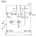
- the circuit 17, having a transfer function according to Eq. 1, may be designed in a plurality of manners readily known to a person skilled in the art. Nevertheless, two exemplary implementations are shown in Figs. 4 and 5. The connections to the supply voltage 12 and to the clock output 14 are indicated.
- R1, R2, R3, and R4 denote resistors
- NMOS and PMOS denote transistors of NMOS and PMOS type, respectively
- U denotes a voltage source
- I 1 and I 2 denote current sources.
- the invention is preferably implemented in a clock amplifier of a GPS navigator device since the jitter and phase jumps seem to be particularly troublesome there.
- the invention is not limited to such implementation, but may be implemented in any kind of device or application using a clock amplifier circuit having similar problems with jitter and phase jumps.
Landscapes
- Physics & Mathematics (AREA)
- Engineering & Computer Science (AREA)
- Computer Hardware Design (AREA)
- Computing Systems (AREA)
- General Engineering & Computer Science (AREA)
- Mathematical Physics (AREA)
- Nonlinear Science (AREA)
- Amplifiers (AREA)
Priority Applications (2)
| Application Number | Priority Date | Filing Date | Title |
|---|---|---|---|
| EP06002881A EP1819047B1 (de) | 2006-02-13 | 2006-02-13 | Schaltung und Verfahren zur Reduzierung von Jitter- und/oder Phasensprung-Problemen in einem Taktsignalverstärkergerät |
| US11/706,076 US20070205813A1 (en) | 2006-02-13 | 2007-02-13 | Circuit and method for reducing jitter and/or phase jump problems in a clock amplifier device |
Applications Claiming Priority (1)
| Application Number | Priority Date | Filing Date | Title |
|---|---|---|---|
| EP06002881A EP1819047B1 (de) | 2006-02-13 | 2006-02-13 | Schaltung und Verfahren zur Reduzierung von Jitter- und/oder Phasensprung-Problemen in einem Taktsignalverstärkergerät |
Publications (2)
| Publication Number | Publication Date |
|---|---|
| EP1819047A1 true EP1819047A1 (de) | 2007-08-15 |
| EP1819047B1 EP1819047B1 (de) | 2012-07-25 |
Family
ID=36659909
Family Applications (1)
| Application Number | Title | Priority Date | Filing Date |
|---|---|---|---|
| EP06002881A Expired - Lifetime EP1819047B1 (de) | 2006-02-13 | 2006-02-13 | Schaltung und Verfahren zur Reduzierung von Jitter- und/oder Phasensprung-Problemen in einem Taktsignalverstärkergerät |
Country Status (2)
| Country | Link |
|---|---|
| US (1) | US20070205813A1 (de) |
| EP (1) | EP1819047B1 (de) |
Cited By (1)
| Publication number | Priority date | Publication date | Assignee | Title |
|---|---|---|---|---|
| CN101499809B (zh) * | 2009-02-16 | 2013-03-13 | 北京星网锐捷网络技术有限公司 | 接收芯片电路与通信系统 |
Families Citing this family (1)
| Publication number | Priority date | Publication date | Assignee | Title |
|---|---|---|---|---|
| CN105897243B (zh) | 2016-03-31 | 2017-06-06 | 中国人民解放军国防科学技术大学 | 一种抗单粒子瞬态的时钟驱动电路 |
Citations (10)
| Publication number | Priority date | Publication date | Assignee | Title |
|---|---|---|---|---|
| US4734597A (en) | 1985-12-07 | 1988-03-29 | Intermetall, Division Of Ditti | CMOS inverter chain |
| EP0601466A2 (de) * | 1992-12-01 | 1994-06-15 | Nec Corporation | Eingangsschaltung zum Empfang von TTL Pegeln |
| US5767728A (en) | 1996-09-05 | 1998-06-16 | International Business Machines Corporation | Noise tolerant CMOS inverter circuit having a resistive bias |
| US6144223A (en) * | 1998-04-03 | 2000-11-07 | Adaptec, Inc. | Integrated circuit SCSI input receiver having precision high speed input buffer with hysteresis |
| US20010054926A1 (en) | 1998-08-14 | 2001-12-27 | Koichiro Minami | Synchronous delay circuit |
| US6335633B1 (en) * | 1997-07-11 | 2002-01-01 | Vanguard International Semiconductor Corporation | Adjustable, full CMOS input buffer for TTL, CMOS, or low swing input protocols |
| US20020075090A1 (en) | 2000-12-20 | 2002-06-20 | Eiichi Hasegawa | Oscillation control circuit |
| US6426661B1 (en) * | 2001-08-20 | 2002-07-30 | International Business Machines Corporation | Clock distribution with constant delay clock buffer circuit |
| US20020190798A1 (en) * | 2001-05-22 | 2002-12-19 | Minoru Kozaki | Ring oscillator circuit and a delay circuit |
| US20050077929A1 (en) * | 2003-08-25 | 2005-04-14 | Infineon Technologies Ag | Driver device, in particular for a semiconductor device, and method for operating a driver device |
Family Cites Families (3)
| Publication number | Priority date | Publication date | Assignee | Title |
|---|---|---|---|---|
| US5163168A (en) * | 1990-03-30 | 1992-11-10 | Matsushita Electric Industrial Co., Ltd. | Pulse signal generator and redundancy selection signal generator |
| SE514936C2 (sv) * | 1999-09-03 | 2001-05-21 | Ericsson Telefon Ab L M | Förfarande och anordning för att förkorta en linjedrivares återhämtningstid |
| US20050113948A1 (en) * | 2003-11-22 | 2005-05-26 | Own Christopher S. | Digital-to-analog audio conversion |
-
2006
- 2006-02-13 EP EP06002881A patent/EP1819047B1/de not_active Expired - Lifetime
-
2007
- 2007-02-13 US US11/706,076 patent/US20070205813A1/en not_active Abandoned
Patent Citations (10)
| Publication number | Priority date | Publication date | Assignee | Title |
|---|---|---|---|---|
| US4734597A (en) | 1985-12-07 | 1988-03-29 | Intermetall, Division Of Ditti | CMOS inverter chain |
| EP0601466A2 (de) * | 1992-12-01 | 1994-06-15 | Nec Corporation | Eingangsschaltung zum Empfang von TTL Pegeln |
| US5767728A (en) | 1996-09-05 | 1998-06-16 | International Business Machines Corporation | Noise tolerant CMOS inverter circuit having a resistive bias |
| US6335633B1 (en) * | 1997-07-11 | 2002-01-01 | Vanguard International Semiconductor Corporation | Adjustable, full CMOS input buffer for TTL, CMOS, or low swing input protocols |
| US6144223A (en) * | 1998-04-03 | 2000-11-07 | Adaptec, Inc. | Integrated circuit SCSI input receiver having precision high speed input buffer with hysteresis |
| US20010054926A1 (en) | 1998-08-14 | 2001-12-27 | Koichiro Minami | Synchronous delay circuit |
| US20020075090A1 (en) | 2000-12-20 | 2002-06-20 | Eiichi Hasegawa | Oscillation control circuit |
| US20020190798A1 (en) * | 2001-05-22 | 2002-12-19 | Minoru Kozaki | Ring oscillator circuit and a delay circuit |
| US6426661B1 (en) * | 2001-08-20 | 2002-07-30 | International Business Machines Corporation | Clock distribution with constant delay clock buffer circuit |
| US20050077929A1 (en) * | 2003-08-25 | 2005-04-14 | Infineon Technologies Ag | Driver device, in particular for a semiconductor device, and method for operating a driver device |
Cited By (1)
| Publication number | Priority date | Publication date | Assignee | Title |
|---|---|---|---|---|
| CN101499809B (zh) * | 2009-02-16 | 2013-03-13 | 北京星网锐捷网络技术有限公司 | 接收芯片电路与通信系统 |
Also Published As
| Publication number | Publication date |
|---|---|
| EP1819047B1 (de) | 2012-07-25 |
| US20070205813A1 (en) | 2007-09-06 |
Similar Documents
| Publication | Publication Date | Title |
|---|---|---|
| EP2346161A1 (de) | Empfangsschaltung | |
| US7701291B2 (en) | Gain improved operational transconductance amplifier and control method thereof | |
| US9148052B2 (en) | Switching regulator with reduced EMI | |
| US20120162189A1 (en) | Driver circuit and video system | |
| US6556039B2 (en) | Impedance adjustment circuit | |
| JP2012123686A (ja) | ボルテージレギュレータ | |
| US10558232B2 (en) | Regulator circuit and control method | |
| US20130027017A1 (en) | Voltage to current converting circuit | |
| US8970275B1 (en) | Process compensated delay line | |
| EP1819047A1 (de) | Schaltung und Verfahren zur Reduzierung von Jitter- und/oder Phasensprung-Problemen in einem Taktsignalverstärkergerät | |
| US20040150434A1 (en) | Low voltage differential signaling driving apparatus | |
| EP1630952B1 (de) | Vorrichtung zur Signalbestimmung welche eine Verstärkerschaltung mit variabler Ansprechgeschwindigkeit enthält | |
| US7843236B2 (en) | Low voltage differential signal receiver | |
| CN113741610B (zh) | 一种基准电压电路及芯片 | |
| US20050089106A1 (en) | Data transmission system and method | |
| US20140129851A1 (en) | Voltage identification definition reference voltage generation circuit and boot voltage generating method thereof | |
| EP3291444A1 (de) | Kompensationsschaltung eines leistungsverstärkers und zugehöriges kompensationsverfahren | |
| US9362873B2 (en) | Instrumentation amplifier | |
| US9564857B2 (en) | Low noise amplifier and chip | |
| US7049876B2 (en) | Level shift circuits and related methods | |
| US20180048266A1 (en) | Amplifier circuit with overshoot suppression | |
| EP3334039B1 (de) | Quellenverfolger | |
| US7692455B2 (en) | Semiconductor devices for receiving a current mode signal and methods of operating the same | |
| US7215173B2 (en) | Low-swing level shifter | |
| US20090128259A1 (en) | Automatic regulator of filter |
Legal Events
| Date | Code | Title | Description |
|---|---|---|---|
| PUAI | Public reference made under article 153(3) epc to a published international application that has entered the european phase |
Free format text: ORIGINAL CODE: 0009012 |
|
| 17P | Request for examination filed |
Effective date: 20070214 |
|
| AK | Designated contracting states |
Kind code of ref document: A1 Designated state(s): AT BE BG CH CY CZ DE DK EE ES FI FR GB GR HU IE IS IT LI LT LU LV MC NL PL PT RO SE SI SK TR |
|
| AX | Request for extension of the european patent |
Extension state: AL BA HR MK YU |
|
| AKX | Designation fees paid |
Designated state(s): DE FR GB |
|
| RAP1 | Party data changed (applicant data changed or rights of an application transferred) |
Owner name: INFINEON TECHNOLOGIES AG |
|
| GRAP | Despatch of communication of intention to grant a patent |
Free format text: ORIGINAL CODE: EPIDOSNIGR1 |
|
| RIC1 | Information provided on ipc code assigned before grant |
Ipc: H03K 19/003 20060101AFI20111212BHEP Ipc: H03K 19/00 20060101ALI20111212BHEP Ipc: G06F 1/10 20060101ALI20111212BHEP |
|
| GRAS | Grant fee paid |
Free format text: ORIGINAL CODE: EPIDOSNIGR3 |
|
| GRAA | (expected) grant |
Free format text: ORIGINAL CODE: 0009210 |
|
| AK | Designated contracting states |
Kind code of ref document: B1 Designated state(s): DE FR GB |
|
| REG | Reference to a national code |
Ref country code: GB Ref legal event code: FG4D |
|
| REG | Reference to a national code |
Ref country code: DE Ref legal event code: R096 Ref document number: 602006030912 Country of ref document: DE Effective date: 20120920 |
|
| PLBE | No opposition filed within time limit |
Free format text: ORIGINAL CODE: 0009261 |
|
| STAA | Information on the status of an ep patent application or granted ep patent |
Free format text: STATUS: NO OPPOSITION FILED WITHIN TIME LIMIT |
|
| 26N | No opposition filed |
Effective date: 20130426 |
|
| REG | Reference to a national code |
Ref country code: DE Ref legal event code: R097 Ref document number: 602006030912 Country of ref document: DE Effective date: 20130426 |
|
| GBPC | Gb: european patent ceased through non-payment of renewal fee |
Effective date: 20130213 |
|
| REG | Reference to a national code |
Ref country code: FR Ref legal event code: ST Effective date: 20131031 |
|
| PG25 | Lapsed in a contracting state [announced via postgrant information from national office to epo] |
Ref country code: FR Free format text: LAPSE BECAUSE OF NON-PAYMENT OF DUE FEES Effective date: 20130228 Ref country code: GB Free format text: LAPSE BECAUSE OF NON-PAYMENT OF DUE FEES Effective date: 20130213 |
|
| PGFP | Annual fee paid to national office [announced via postgrant information from national office to epo] |
Ref country code: DE Payment date: 20190426 Year of fee payment: 14 |
|
| REG | Reference to a national code |
Ref country code: DE Ref legal event code: R119 Ref document number: 602006030912 Country of ref document: DE |
|
| PG25 | Lapsed in a contracting state [announced via postgrant information from national office to epo] |
Ref country code: DE Free format text: LAPSE BECAUSE OF NON-PAYMENT OF DUE FEES Effective date: 20200901 |