EP1819145A2 - Dispositif CCD - Google Patents
Dispositif CCD Download PDFInfo
- Publication number
- EP1819145A2 EP1819145A2 EP07250602A EP07250602A EP1819145A2 EP 1819145 A2 EP1819145 A2 EP 1819145A2 EP 07250602 A EP07250602 A EP 07250602A EP 07250602 A EP07250602 A EP 07250602A EP 1819145 A2 EP1819145 A2 EP 1819145A2
- Authority
- EP
- European Patent Office
- Prior art keywords
- charge
- register
- gain
- elements
- multiplication
- Prior art date
- Legal status (The legal status is an assumption and is not a legal conclusion. Google has not performed a legal analysis and makes no representation as to the accuracy of the status listed.)
- Withdrawn
Links
Images


Classifications
-
- H—ELECTRICITY
- H10—SEMICONDUCTOR DEVICES; ELECTRIC SOLID-STATE DEVICES NOT OTHERWISE PROVIDED FOR
- H10F—INORGANIC SEMICONDUCTOR DEVICES SENSITIVE TO INFRARED RADIATION, LIGHT, ELECTROMAGNETIC RADIATION OF SHORTER WAVELENGTH OR CORPUSCULAR RADIATION
- H10F39/00—Integrated devices, or assemblies of multiple devices, comprising at least one element covered by group H10F30/00, e.g. radiation detectors comprising photodiode arrays
- H10F39/10—Integrated devices
- H10F39/12—Image sensors
- H10F39/15—Charge-coupled device [CCD] image sensors
- H10F39/153—Two-dimensional or three-dimensional array CCD image sensors
-
- H—ELECTRICITY
- H04—ELECTRIC COMMUNICATION TECHNIQUE
- H04N—PICTORIAL COMMUNICATION, e.g. TELEVISION
- H04N25/00—Circuitry of solid-state image sensors [SSIS]; Control thereof
-
- H—ELECTRICITY
- H04—ELECTRIC COMMUNICATION TECHNIQUE
- H04N—PICTORIAL COMMUNICATION, e.g. TELEVISION
- H04N25/00—Circuitry of solid-state image sensors [SSIS]; Control thereof
- H04N25/70—SSIS architectures; Circuits associated therewith
- H04N25/71—Charge-coupled device [CCD] sensors; Charge-transfer registers specially adapted for CCD sensors
- H04N25/713—Transfer or readout registers; Split readout registers or multiple readout registers
-
- H—ELECTRICITY
- H04—ELECTRIC COMMUNICATION TECHNIQUE
- H04N—PICTORIAL COMMUNICATION, e.g. TELEVISION
- H04N25/00—Circuitry of solid-state image sensors [SSIS]; Control thereof
- H04N25/70—SSIS architectures; Circuits associated therewith
- H04N25/71—Charge-coupled device [CCD] sensors; Charge-transfer registers specially adapted for CCD sensors
- H04N25/72—Charge-coupled device [CCD] sensors; Charge-transfer registers specially adapted for CCD sensors using frame transfer [FT]
-
- H—ELECTRICITY
- H10—SEMICONDUCTOR DEVICES; ELECTRIC SOLID-STATE DEVICES NOT OTHERWISE PROVIDED FOR
- H10F—INORGANIC SEMICONDUCTOR DEVICES SENSITIVE TO INFRARED RADIATION, LIGHT, ELECTROMAGNETIC RADIATION OF SHORTER WAVELENGTH OR CORPUSCULAR RADIATION
- H10F39/00—Integrated devices, or assemblies of multiple devices, comprising at least one element covered by group H10F30/00, e.g. radiation detectors comprising photodiode arrays
- H10F39/10—Integrated devices
- H10F39/12—Image sensors
- H10F39/15—Charge-coupled device [CCD] image sensors
- H10F39/153—Two-dimensional or three-dimensional array CCD image sensors
- H10F39/1536—Frame transfer
-
- H—ELECTRICITY
- H04—ELECTRIC COMMUNICATION TECHNIQUE
- H04N—PICTORIAL COMMUNICATION, e.g. TELEVISION
- H04N23/00—Cameras or camera modules comprising electronic image sensors; Control thereof
- H04N23/50—Constructional details
- H04N23/555—Constructional details for picking-up images in sites, inaccessible due to their dimensions or hazardous conditions, e.g. endoscopes or borescopes
Definitions
- the present invention relates to a CCD device, and in particular to a CCD which provides gain within the charge domain.
- signal charge representative of incident radiation is accumulated in an array of pixels in an image area. Following an integration period, signal charge is transferred to a store section and then to an output register by applying appropriate clocking or drive pulses to control electrodes. The signal charge is then read out from the output register and applied to a charge detection circuit to produce a voltage that is representative of the amount of signal charge.
- the sensitivity of such a device is limited by the noise of the charge to voltage conversion process and that introduced by the subsequent video chain electronics.
- a CCD imager 1 comprises an image area 2, a store section 3 and an output or read-out register 4, each of these components being found in a conventional CCD imager.
- the output register 4 is extended serially to give a multiplication register 5, the output of which is connected to a charge detection circuit 6.
- incident radiation is converted at the image area 2 into signal charge which is representative of the intensity of the radiation impinging on the array of pixels making up the image array.
- drive pulses are applied to control electrodes 7 to transfer the charge accumulated at the pixels of the image area 2 to the store section 3.
- drive signals are also applied to control electrodes 8 at the store section 3 to cause charge to be transferred from row to row as indicated by the arrow, the last row of charge held in elements in row 3 being transferred in parallel to the output register 4.
- the multiplication register is of similar architecture to the output register in so far as doping is concerned with the addition of an electrode for multiplication.
- the output of the charge detection circuit 6 is also applied to an automatic gain control circuit 11 that adjusts the voltages applied to the multiplication register 5 to control the gain. In other embodiments, this feedback arrangement is omitted. Gain may then be controlled manually if desired.
- the gain control circuit can vary the gain provided by varying the voltages applied to the multiplication register, we have appreciated the need to determine the actual level of gain provided by such a CCD charge multiplication arrangement.
- One way to measure the gain is to arrange a structure in the multiplication register to allow direct injection of charge, which can then be measured at the output. The difficulty with this approach is that the amount of charge injected cannot be precisely defined.
- the approach usually taken to measure the gain is to illuminate the device and to measure the output with no multiplication gain.
- the light level is then reduced by a known fraction (by reducing the aperture of the optics or using neutral density filters for example).
- the reduction of light level will be of the same order as the gain to be measured.
- Multiplication gain is then applied and the output signal is measured.
- the multiplication gain can be calculated knowing the output signal and the reduction in light level. This method can give accurate results but is cumbersome and not particularly suitable for automatic measurements within a camera system.
- the invention determines the gain provided by a multiplication register by measuring an output signal derived from a first input signal with gain applied to the multiplication register and measuring an output derived from a second input signal without gain applied.
- There are two approaches to generating the two output signals which may be used alone or in combination.
- a first approach is to vary the input signal to the multiplication register, such as by summing charge at the input.
- a second approach is to vary the output signal from the multiplication register, such as by summing charge at the output. In either approach, the second output signal is effectively larger than the first output signal by a known amount.
- the gain provided can then be determined as a function of the ratios of the output signals.
- the preferred embodiment of the invention provides various techniques for creating the first and second input signals such that the second signal is known to be effectively larger than the first by a known amount.
- a first technique embodying the invention is to sum charge accumulated in a plurality of elements to provide the second input signal (though the summing may be at an output, rather than an input as noted above) and to derive the first signal from one such element or by averaging (rather than summing) the charge in the plurality of elements. This creates a second input signal that is effectively a multiple of the first signal; the multiple being equal to the number of elements.
- a second technique in a camera embodying the invention, is to provide first and second input signals to the multiplication register by illuminating light sensitive elements before the multiplication register using a light source within the camera of first and second different illumination strengths to produce the first and second respective input signals.
- the second input signal may typically be effectively 3 orders of magnitude greater than the first input signal.
- the multiplication register provides gain of around 1,000, so the output signals will be similar with and without gain. The actual gain provided can then be determined from the ratio of the input signals. When using lower gains such as x10, it is preferable to sum charge at the input to the multiplication register to ensure an adequate output signal.
- a benefit of the arrangements embodying the invention is that the gain can be measured real-time during operation of a camera embodying the invention.
- Existing electron multiplier CCD based cameras have no provision for determination of actual gain value. This can lead to various compromises in the camera performance since gain has to be estimated from knowledge of the applied voltage on the CCD Gain phase.
- the Voltage / Gain transfer function is extremely non-linear, and the voltage required to produce a particular Gain value will vary as a function of both time and temperature. In order to maintain optimal camera performance it becomes necessary to age the cameras for 100 hours prior to shipment, and to re-calibrate after approximately 1000 hours. This can be very inconvenient, particularly where the camera has been installed in an in-accessible location.
- the existing designs only allow the user to observe a 16bit digital number, which is broadly indicative of gain, but which only has limited value for short-term comparison between related measurements. Embodiments of the invention overcome these problems.
- the adjustment of gain is preferably provided by adjusting the phase relationship between electrodes in the multiplication register. This has the advantage that gain can be adjusted rapidly for calibration, whilst allowing the gain to be restored precisely to the original operational level. Alternatively, the gain could be varied by adjusting the voltage between electrodes.
- the embodiments provide automatic measurement of gain in real-time; the main embodiment using thermally generated charge as a signal source.
- a camera embodying the invention is designed to allow this calibration to take place during field blanking intervals.
- a known device is shown and has been described in relation to Figure 1.
- the invention may be embodied in such a device, and in an imager or camera including such a device.
- the arrangement of a multiplication register and elements within that register to which the invention may be applied will first be described with reference to figures 1 to 3.
- an image area 2 accumulates charge in CCD elements and transfers charge under control of clocked drive pulses on electrodes 7, 8 to a store area 3 and from the store area to an output register 4 and subsequently to a multiplication register 5. It is in the multiplication register that the invention is embodied, though it will be appreciated that other arrangements of multiplication elements could be used. Although shown as a straight-line extension of the output register 4, in reality it may be bent around the imager for packaging reasons.
- a multiplication element of known type is shown in Figure 2.
- the element comprises a base 20 of p-type silicon, an n-type layer 22 and a gate dielectric layer 24 which may, as an example, comprise a layer of Si3N4 over SiO2 or SiO2 only.
- a gate dielectric layer 24 which may, as an example, comprise a layer of Si3N4 over SiO2 or SiO2 only.
- each element has four electrodes shown as normal clocked electrodes ⁇ 1 26 and ⁇ 3 28, a DC electrode ⁇ DC 30 and a high voltage electrode ⁇ 2HV 32.
- the element provides gain by clocking voltages at the electrodes such that a relatively high voltage at electrode ⁇ HV 32 causes impact ionisation of charge.
- FIG. 3 A schematic cross section of a single multiplication element is given in Figure 3.
- the multiplication element of the multiplication register is made up of four phases although other configurations could be possible.
- ⁇ 1 and ⁇ 3 are clocked as normal readout register phases.
- ⁇ DC is a DC phase that separates ⁇ 1 from ⁇ 2.
- the high voltage electrode ⁇ 2, the multiplication phase is a clocked phase but using a much greater amplitude than ⁇ 1 and ⁇ 3.
- the signal originally under ⁇ 1 will drift to ⁇ 2.
- the potential on ⁇ 2 is set high enough so that the fields experienced by the electron signal will cause impact ionisation to take place.
- the total amplified signal can then be transferred to ⁇ by switching ⁇ 2 low and ⁇ high.
- the process is repeated through all the gain (multiplication) elements in the multiplication register.
- the embodiment of Figure 5 makes use of thermal charge accumulated as a mechanism of providing a known ratio of signals.
- an image area 2 accumulates charge in CCD elements and transfers charge under control of clocked drive pulses on electrodes 7, 8 to a store area 3 and from the store area to an output register 4 and subsequently to a multiplication register 5.
- the camera operates as follows. When the last line of a previous field has been transferred from the store area 3 to the output register 4, the adjacent line in the store section will contain thermal charge accumulated over the field readout interval - typically 20ms for CCIR cameras. The thermal charge accumulated in this period is then transferred into the readout register 4. The gain provided by the multiplication register is maintained at a given value, and the pixels are readout normally.
- the camera processor 40 has a function to average all the pixels to obtain a single value (S gain). The data from all pixels may be assessed further to gain confidence that the observed standard deviation is consistent with the calculated mean value.
- the following line which will contain a similar amount of dark current, is then transferred to the readout register 4, the gain of the multiplication register 5 is adjusted to apply unity gain, all pixels in the line are then summed in an output node of the CCD shown as the processor 40, and readout as a single value (S unity).
- the processor 40 now has two output values: S gain derived from the mean value of a charge due to thermal electrons in a single element with gain applied; and S unity derived from the sum of charge in all the elements of the readout register without gain applied. S unity is thus the average charge in each element of the readout register x the number of pixels in the line of the readout register. Summing ensures that the very small thermally generated signal will exceed the output node readout noise. It is noted that the summing could be done before or after the multiplication register and has the effect of creating an output signal which is, in effect, derived from the sum of the charge input to the multiplication register.
- This figure may then be used to make automatic adjustment of gain limits, to determine when filters should be applied to the image, and for presentation to the user as an absolute gain value.
- the technique described allows acquisition of an updated gain value at each field period. Since the gain control voltage is arranged to be very stable over a few hundred milliseconds it may be advantageous to measure gain value for several fields and then compute the average.
- the CCD will typically be operating at temperatures of -5°C, or lower. In the embodiment, this would produce of the order 1 electron/pixel/field. With roughly 600 pixels in each line, this will result in 600 electrons at the output node, which is just about adequate to overcome the node readout noise.
- a further enhancement where the electron levels are low is to produce the S unity signal by "binning" a few lines into the readout register.
- the process of "binning” means summing a few lines from the store area 3 into the readout/ output register 4 thereby producing more electrons. If this is done, the equation above is modified to include the number of lines binned as a multiplier.
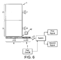
- a second embodiment is shown in Figure 6 and is based on the principles of the first, namely providing two respective input signals to the multiplication register that are orders of magnitude apart (by a known amount) and measuring the ratio of the output signals with and without gain respectively.
- a light source such as an LED 42 is located so as to illuminate a light sensitive region prior to the input end of the multiplication register.
- the operation is then as follows. First, the LED illuminates the light sensitive region with a low level (or for a short time) to produce a low charge. This low charge is clocked through the multiplication register with normal gain applied to produce a signal S gain. Then, the LED illuminates the sensitive region with a high level (or for a longer time) to produce a high charge. This high charge is clocked through the multiplication register without gain applied to produce a signal S unity.
- a minimum of two line periods will typically be required for readout of the charge.
- the use of the illuminating LED allows the ratio of charge for the two signals to be precisely controlled. This assumes that it is possible to adjust gain rapidly in the inter-line interval.
- the embodying circuit generating the control voltage has been designed to be very stable, and it is therefore preferable not to change the amplitude rapidly of any of the clocking signals (this approach would require the amplitude to be restored very precisely to within a few millivolts).
- gain is also dependent upon the phase relationship between ⁇ 1 and ⁇ 2HV phases, and the clock sequencer can control phase, virtually instantaneously. Accordingly, this is the preferred mechanism to reduce gain of the multiplication register to unity in either the first or second embodiment.
- a camera embodying the invention comprises a lens arrangement for imaging light onto a CCD device of the type previously described and output electronics for processing signals from the CCD device.
Landscapes
- Engineering & Computer Science (AREA)
- Multimedia (AREA)
- Signal Processing (AREA)
- Transforming Light Signals Into Electric Signals (AREA)
- Solid State Image Pick-Up Elements (AREA)
Applications Claiming Priority (1)
| Application Number | Priority Date | Filing Date | Title |
|---|---|---|---|
| GB0602965A GB2435126A (en) | 2006-02-14 | 2006-02-14 | EMCCD device with multiplication register gain measurement allowing realtime calibration of a camera in use. |
Publications (2)
| Publication Number | Publication Date |
|---|---|
| EP1819145A2 true EP1819145A2 (fr) | 2007-08-15 |
| EP1819145A3 EP1819145A3 (fr) | 2008-05-28 |
Family
ID=36141821
Family Applications (1)
| Application Number | Title | Priority Date | Filing Date |
|---|---|---|---|
| EP07250602A Withdrawn EP1819145A3 (fr) | 2006-02-14 | 2007-02-14 | Dispositif CCD |
Country Status (3)
| Country | Link |
|---|---|
| US (1) | US7807952B2 (fr) |
| EP (1) | EP1819145A3 (fr) |
| GB (1) | GB2435126A (fr) |
Cited By (2)
| Publication number | Priority date | Publication date | Assignee | Title |
|---|---|---|---|---|
| EP2034716A3 (fr) * | 2007-09-07 | 2012-10-24 | E2V Technologies (UK) Limited | Procédé pour déterminer le gain à l'aide de signaux de sortie |
| EP2571254A4 (fr) * | 2010-05-14 | 2014-06-25 | Hamamatsu Photonics Kk | Procédé destiné à mesurer un facteur de multiplication électronique |
Families Citing this family (12)
| Publication number | Priority date | Publication date | Assignee | Title |
|---|---|---|---|---|
| JP2008271049A (ja) * | 2007-04-18 | 2008-11-06 | Hamamatsu Photonics Kk | 撮像装置及びそのゲイン調整方法 |
| FR2924862B1 (fr) * | 2007-12-10 | 2010-08-13 | Commissariat Energie Atomique | Dispositif microelectronique photosensible avec multiplicateurs par avalanche |
| US8773564B2 (en) | 2010-12-14 | 2014-07-08 | Truesense Imaging, Inc. | Image sensor with charge multiplication |
| US8479374B2 (en) | 2010-12-14 | 2013-07-09 | Truesense Imaging, Inc. | Method of producing an image sensor having multiple output channels |
| US8493492B2 (en) | 2010-12-14 | 2013-07-23 | Truesense Imaging, Inc. | Method of producing an image with pixel signals produced by an image sensor that includes multiple output channels |
| US8493491B2 (en) | 2010-12-14 | 2013-07-23 | Truesense Imaging, Inc. | Methods for processing an image captured by an image sensor having multiple output channels |
| US8553126B2 (en) | 2010-12-14 | 2013-10-08 | Truesense Imaging, Inc. | Image sensor with charge multiplication |
| CN102158661B (zh) * | 2011-01-26 | 2012-09-19 | 中国科学院长春光学精密机械与物理研究所 | 一种emccd特有信号的驱动系统 |
| GB201516701D0 (en) * | 2015-09-21 | 2015-11-04 | Innovation & Business Dev Solutions Ltd | Time of flight distance sensor |
| US9930276B2 (en) | 2016-01-14 | 2018-03-27 | Semiconductor Components Industries, Llc | Methods for clocking an image sensor |
| GB201704452D0 (en) | 2017-03-21 | 2017-05-03 | Photonic Vision Ltd | Time of flight sensor |
| CN111988546B (zh) * | 2020-09-15 | 2023-03-31 | 哈尔滨工程大学 | 一种倍增ccd倍增增益及读出噪声测量方法 |
Family Cites Families (14)
| Publication number | Priority date | Publication date | Assignee | Title |
|---|---|---|---|---|
| US4585934A (en) * | 1979-03-05 | 1986-04-29 | Hughes Aircraft Company | Self-calibration technique for charge-coupled device imagers |
| KR100298039B1 (ko) | 1991-07-11 | 2001-10-24 | 윌리엄 비. 켐플러 | 전하증배장치및그제조방법 |
| GB2323471B (en) | 1997-03-22 | 2002-04-17 | Eev Ltd | CCd imagers |
| GB9828166D0 (en) | 1998-12-22 | 1999-02-17 | Eev Ltd | Imaging apparatus |
| US7420605B2 (en) * | 2001-01-18 | 2008-09-02 | E2V Technologies (Uk) Limited | Solid state imager arrangements |
| GB2371403B (en) | 2001-01-18 | 2005-07-27 | Marconi Applied Techn Ltd | Solid state imager arrangements |
| JP2003009000A (ja) * | 2001-06-21 | 2003-01-10 | Fuji Photo Film Co Ltd | 撮像装置 |
| US7184085B2 (en) | 2001-08-20 | 2007-02-27 | Fuji Photo Film Co., Ltd. | Charge multiplying solid-state electronic image sensing device and method of controlling same |
| JP3689866B2 (ja) | 2002-05-30 | 2005-08-31 | 日本テキサス・インスツルメンツ株式会社 | Cmd及びcmd搭載ccd装置 |
| GB0316994D0 (en) | 2003-07-21 | 2003-08-27 | E2V Tech Uk Ltd | Smear reduction in CCD images |
| GB2413007A (en) * | 2004-04-07 | 2005-10-12 | E2V Tech Uk Ltd | Multiplication register for amplifying signal charge |
| GB0501149D0 (en) | 2005-01-20 | 2005-02-23 | Andor Technology Plc | Automatic calibration of electron multiplying CCds |
| GB2424758A (en) | 2005-03-31 | 2006-10-04 | E2V Tech | CCD device |
| DE102006000976A1 (de) | 2006-01-07 | 2007-07-12 | Leica Microsystems Cms Gmbh | Vorrichtung, Mikroskop mit Vorrichtung und Verfahren zum Kalibrieren eines Photosensor-Chips |
-
2006
- 2006-02-14 GB GB0602965A patent/GB2435126A/en not_active Withdrawn
-
2007
- 2007-02-14 EP EP07250602A patent/EP1819145A3/fr not_active Withdrawn
- 2007-02-14 US US11/705,821 patent/US7807952B2/en not_active Expired - Fee Related
Cited By (3)
| Publication number | Priority date | Publication date | Assignee | Title |
|---|---|---|---|---|
| EP2034716A3 (fr) * | 2007-09-07 | 2012-10-24 | E2V Technologies (UK) Limited | Procédé pour déterminer le gain à l'aide de signaux de sortie |
| EP2571254A4 (fr) * | 2010-05-14 | 2014-06-25 | Hamamatsu Photonics Kk | Procédé destiné à mesurer un facteur de multiplication électronique |
| US9142591B2 (en) | 2010-05-14 | 2015-09-22 | Hamamatsu Photonics K.K. | Method for measuring electronic multiplication factor |
Also Published As
| Publication number | Publication date |
|---|---|
| US20070214200A1 (en) | 2007-09-13 |
| EP1819145A3 (fr) | 2008-05-28 |
| GB0602965D0 (en) | 2006-03-29 |
| GB2435126A (en) | 2007-08-15 |
| US7807952B2 (en) | 2010-10-05 |
Similar Documents
| Publication | Publication Date | Title |
|---|---|---|
| EP1819145A2 (fr) | Dispositif CCD | |
| US8054363B2 (en) | Determining the multiplication of EMCCD sensor | |
| JP4536901B2 (ja) | 拡大されたダイナミックレンジを有するcmosイメージセンサ | |
| US9609243B2 (en) | Systems and methods for providing low-noise readout of an optical sensor | |
| KR100659443B1 (ko) | X-y 어드레스가능 mos 화상 형성 장치 사용 방법, 화상 감지용 제품 및 x-y 어드레스가능 mos 화상 형성 장치 시스템 | |
| JP5319872B2 (ja) | 電子増倍ccdの自動較正 | |
| JP5291287B2 (ja) | 利得計測構造体 | |
| CN109155827B (zh) | 高动态范围成像传感器阵列 | |
| US20030117386A1 (en) | Solid state imaging apparatus and method for driving the same | |
| GB2328338A (en) | Temperature dependent dark current correction in imaging apparatus | |
| Goebel et al. | Overview of the SAPHIRA detector for adaptive optics applications | |
| EP3447461A1 (fr) | Élément d'imagerie infrarouge et caméra infrarouge | |
| EP1943831B1 (fr) | Capteur d'image | |
| CA2451463C (fr) | Procede et dispositif de lecture de matrices microbolometriques composees | |
| EP2359588B1 (fr) | Capteurs d'images dotés d'écrans non uniformes | |
| US6992713B2 (en) | Fully integrated solid state imager and camera display | |
| US5642162A (en) | Charge transfer device having a signal processing circuit for correcting output voltage | |
| US4562473A (en) | Dark current sensing with a solid-state imager having a CCD line register output | |
| US20040135913A1 (en) | Output-compensating device and method of an image sensor | |
| JP2016220037A (ja) | 高ダイナミックレンジ撮像装置及び撮像方法 | |
| JPS61144174A (ja) | 固体撮像装置 | |
| Mooney | 1/f noise measurements on PtSi focal plane arrays | |
| JP2555247Y2 (ja) | 画像読み取り装置 | |
| JPH06113191A (ja) | ビデオ・カメラおよびその測光方法 | |
| JP2004333132A (ja) | 熱型赤外線固体撮像装置 |
Legal Events
| Date | Code | Title | Description |
|---|---|---|---|
| PUAI | Public reference made under article 153(3) epc to a published international application that has entered the european phase |
Free format text: ORIGINAL CODE: 0009012 |
|
| AK | Designated contracting states |
Kind code of ref document: A2 Designated state(s): AT BE BG CH CY CZ DE DK EE ES FI FR GB GR HU IE IS IT LI LT LU LV MC NL PL PT RO SE SI SK TR |
|
| AX | Request for extension of the european patent |
Extension state: AL BA HR MK YU |
|
| PUAL | Search report despatched |
Free format text: ORIGINAL CODE: 0009013 |
|
| AK | Designated contracting states |
Kind code of ref document: A3 Designated state(s): AT BE BG CH CY CZ DE DK EE ES FI FR GB GR HU IE IS IT LI LT LU LV MC NL PL PT RO SE SI SK TR |
|
| AX | Request for extension of the european patent |
Extension state: AL BA HR MK RS |
|
| 17P | Request for examination filed |
Effective date: 20081125 |
|
| AKX | Designation fees paid |
Designated state(s): AT BE BG CH CY CZ DE DK EE ES FI FR GB GR HU IE IS IT LI LT LU LV MC NL PL PT RO SE SI SK TR |
|
| 17Q | First examination report despatched |
Effective date: 20090126 |
|
| STAA | Information on the status of an ep patent application or granted ep patent |
Free format text: STATUS: THE APPLICATION IS DEEMED TO BE WITHDRAWN |
|
| 18D | Application deemed to be withdrawn |
Effective date: 20090806 |