EP1820268B1 - Spannungsklemme zur verbesserten einschwingleistung eines kollektorspannungsgesteuerten leistungsverstärkers - Google Patents
Spannungsklemme zur verbesserten einschwingleistung eines kollektorspannungsgesteuerten leistungsverstärkers Download PDFInfo
- Publication number
- EP1820268B1 EP1820268B1 EP05852811.8A EP05852811A EP1820268B1 EP 1820268 B1 EP1820268 B1 EP 1820268B1 EP 05852811 A EP05852811 A EP 05852811A EP 1820268 B1 EP1820268 B1 EP 1820268B1
- Authority
- EP
- European Patent Office
- Prior art keywords
- voltage
- signal
- transistor
- power amplifier
- responsive
- Prior art date
- Legal status (The legal status is an assumption and is not a legal conclusion. Google has not performed a legal analysis and makes no representation as to the accuracy of the status listed.)
- Expired - Lifetime
Links
Images



Classifications
-
- H—ELECTRICITY
- H03—ELECTRONIC CIRCUITRY
- H03G—CONTROL OF AMPLIFICATION
- H03G3/00—Gain control in amplifiers or frequency changers
- H03G3/20—Automatic control
-
- H—ELECTRICITY
- H03—ELECTRONIC CIRCUITRY
- H03F—AMPLIFIERS
- H03F1/00—Details of amplifiers with only discharge tubes, only semiconductor devices or only unspecified devices as amplifying elements
- H03F1/02—Modifications of amplifiers to raise the efficiency, e.g. gliding Class A stages, use of an auxiliary oscillation
- H03F1/0205—Modifications of amplifiers to raise the efficiency, e.g. gliding Class A stages, use of an auxiliary oscillation in transistor amplifiers
- H03F1/0211—Modifications of amplifiers to raise the efficiency, e.g. gliding Class A stages, use of an auxiliary oscillation in transistor amplifiers with control of the supply voltage or current
- H03F1/0216—Continuous control
- H03F1/0222—Continuous control by using a signal derived from the input signal
- H03F1/0227—Continuous control by using a signal derived from the input signal using supply converters
-
- H—ELECTRICITY
- H03—ELECTRONIC CIRCUITRY
- H03F—AMPLIFIERS
- H03F1/00—Details of amplifiers with only discharge tubes, only semiconductor devices or only unspecified devices as amplifying elements
- H03F1/02—Modifications of amplifiers to raise the efficiency, e.g. gliding Class A stages, use of an auxiliary oscillation
- H03F1/0205—Modifications of amplifiers to raise the efficiency, e.g. gliding Class A stages, use of an auxiliary oscillation in transistor amplifiers
- H03F1/0211—Modifications of amplifiers to raise the efficiency, e.g. gliding Class A stages, use of an auxiliary oscillation in transistor amplifiers with control of the supply voltage or current
- H03F1/0244—Stepped control
-
- H—ELECTRICITY
- H03—ELECTRONIC CIRCUITRY
- H03F—AMPLIFIERS
- H03F1/00—Details of amplifiers with only discharge tubes, only semiconductor devices or only unspecified devices as amplifying elements
- H03F1/34—Negative-feedback-circuit arrangements with or without positive feedback
-
- H—ELECTRICITY
- H03—ELECTRONIC CIRCUITRY
- H03G—CONTROL OF AMPLIFICATION
- H03G3/00—Gain control in amplifiers or frequency changers
- H03G3/004—Control by varying the supply voltage
-
- H—ELECTRICITY
- H03—ELECTRONIC CIRCUITRY
- H03G—CONTROL OF AMPLIFICATION
- H03G3/00—Gain control in amplifiers or frequency changers
- H03G3/20—Automatic control
- H03G3/30—Automatic control in amplifiers having semiconductor devices
- H03G3/3036—Automatic control in amplifiers having semiconductor devices in high-frequency amplifiers or in frequency-changers
- H03G3/3042—Automatic control in amplifiers having semiconductor devices in high-frequency amplifiers or in frequency-changers in modulators, frequency-changers, transmitters or power amplifiers
- H03G3/3047—Automatic control in amplifiers having semiconductor devices in high-frequency amplifiers or in frequency-changers in modulators, frequency-changers, transmitters or power amplifiers for intermittent signals, e.g. burst signals
-
- H—ELECTRICITY
- H03—ELECTRONIC CIRCUITRY
- H03F—AMPLIFIERS
- H03F2200/00—Indexing scheme relating to amplifiers
- H03F2200/504—Indexing scheme relating to amplifiers the supply voltage or current being continuously controlled by a controlling signal, e.g. the controlling signal of a transistor implemented as variable resistor in a supply path for, an IC-block showed amplifier
Definitions
- a portable communication device includes one or more power amplifiers for amplifying the power of the signal to be transmitted from the portable communication device.
- a collector voltage controlled power amplifier PA
- the output power is determined by a regulated voltage applied to the collector of a bipolar junction transistor (or drain, if implemented as a field effect transistor (FET)) of one or more stages of the power amplifier.
- the voltage V ENV controls the power amplifier as a function of the peak voltage of the power amplifier determined during calibration, and corresponds to power amplifier output power.
- An example of an amplifier where the supply voltage tracks the input envelope signal can be found in patent document US 2004/01857803 .
- a power amplifier requires a relatively large current source.
- a relatively large transistor typically a field effect transistor (FET)
- FET field effect transistor
- Embodiments of the invention include a method for dynamically controlling an envelope and power output of a power amplifier, comprising: providing a radio frequency signal to a power amplifier; generating an envelope control signal; generating a voltage clamp signal; generating a regulated voltage , the regulated voltage being related to the envelope control signal; supplying the regulated voltage to the power amplifier; controlling an output of the power amplifier according to the regulated voltage, the regulated voltage being responsive to the envelope control signal and the voltage clamp signal; preventing the regulated voltage from being responsive to a signal other than the voltage clamp signal when the envelope control signal exceeds a level of the voltage clamp signal; and controlling the transition of the regulated voltage from being responsive to the envelope control signal to being responsive to the voltage clamp signal by gradually transitioning the regulated voltage between being responsive to the envelope control signal to being responsive to the voltage clamp signal.
- Embodiments of the invention also include a power control circuit for a power amplifier comprising: means for providing a radio frequency signal to a power amplifier; means for generating an envelope control signal ; means for generating a voltage clamp signal ; means for generating a regulated voltage , the regulated voltage being related to the envelope control signal; means for supplying the regulated voltage to the power amplifier; means for controlling an output of the power amplifier according to the regulated voltage, the regulated voltage being responsive to the envelope control signal and the voltage clamp signal; means for preventing the regulated voltage from being responsive to a signal other than the voltage clamp signal when the envelope control signal exceeds a level of the voltage clamp signal; and means for controlling the transition of the regulated voltage from being responsive to the envelope control signal to being responsive to the voltage clamp signal by gradually transitioning the regulated voltage between being responsive to the envelope control signal to being responsive to the voltage clamp signal.
- Embodiments of the invention also include a portable transceiver comprising a transceiver capable of transmitting and receiving a radio frequency signal and a power control circuit as described above.
- the software for the power amplifier control element comprises an ordered listing of executable instructions for implementing logical functions, and can be embodied in any computer-readable medium for use by or in connection with an instruction execution system, apparatus, or device, such as a computer-based system, processor-containing system, or other system that can fetch the instructions from the instruction execution system, apparatus, or device and execute the instructions.
- a "computer-readable medium” can be any means that can contain, store, communicate, propagate, or transport the program for use by or in connection with the instruction execution system, apparatus, or device.
- the computer readable medium can be, for example but not limited to, an electronic, magnetic, optical, electromagnetic, infrared, or semiconductor system, apparatus, device, or propagation medium.
- FIG. 1 is a block diagram illustrating a simplified portable transceiver 100 including a power amplifier control element having a voltage regulator in accordance with an embodiment of the invention.
- the portable transceiver 100 includes speaker 102, display 104, keyboard 106, and microphone 108, all connected to baseband subsystem 110.
- a power source 142 which may be a direct current (DC) battery or other power source, is also connected to the baseband subsystem 110 via connection 144 to provide power to the portable transceiver 100.
- portable transceiver 100 can be, for example but not limited to, a portable telecommunication device such as a mobile cellular-type telephone.
- Speaker 102 and display 104 receive signals from baseband subsystem 110 via connections 112 and 114, respectively, as known to those skilled in the art. Similarly, keyboard 106 and microphone 108 supply signals to baseband subsystem 110 via connections 116 and 118, respectively.
- Baseband subsystem 110 includes microprocessor ( ⁇ P) 120, memory 122, analog circuitry 124, and digital signal processor (DSP) 126 in communication via bus 128.
- ⁇ P microprocessor
- DSP digital signal processor
- the baseband subsystem 110 may also include an application specific integrated circuit (ASIC) 135 and /or a field programmable gate array (FPGA) 133.
- ASIC application specific integrated circuit
- FPGA field programmable gate array
- Microprocessor 120 and memory 122 provide the signal timing, processing and storage functions for portable transceiver 100.
- Analog circuitry 124 provides the analog processing functions for the signals within baseband subsystem 110.
- Baseband subsystem 110 provides control signals to transmitter 150 and receiver 170 via connection 132 and provides an envelope control signal, referred to as V ENV , to a power amplifier control module 210 via connection 146.
- the signal V ENV is generated by the baseband subsystem 110 and is generally converted to an analog control signal by one of the digital-to-analog converters (DACs) 136 or 138 to be described below.
- the signal V ENV is illustrated as being supplied from the bus 128 to indicate that the signal may be generated in different ways as known to those skilled in the art.
- the voltage V ENV controls the power amplifier as a function of the peak voltage of the power amplifier determined during calibration, and corresponds to power amplifier output power.
- the control signals on connections 132 and 146 may originate from the DSP 126, the ASIC 135, the FPGA 133, or from microprocessor 120, and are supplied to a variety of connections within the transmitter 150, receiver 170 and the power amplifier control module 210. It should be noted that, for simplicity, only the basic components of portable transceiver 100 are illustrated herein.
- the control signals provided by the baseband subsystem 110 control the various components within the transmitter 150 and the receiver 170. Further, the function of the transmitter 150 and the receiver 170 may be integrated into a transceiver.
- the transmitter 150 includes modulator 152, which modulates the analog information on connection 140 and provides a modulated signal via connection 158 to upconverter 154.
- the upconverter 154 transforms the modulated signal on connection 158 to an appropriate transmit frequency and provides the upconverted signal to a power amplifier 180 via connection 184.
- the power amplifier 180 and the power amplifier control module 210 form a power amplifier module 200 ( FIG. 2 ).
- the power amplifier 180 amplifies the signal to an appropriate power level for the system in which the portable transceiver 100 is designed to operate.
- the cartesian in-phase (I) and quadrature (Q) components of the transmit signal are converted to their polar counterparts, amplitude and phase.
- the phase modulation is performed by the modulator 152, while the amplitude modulation is performed by the power control module 210, where the amplitude envelope is defined by the voltage V ENV , and the instantaneous power level of the power amplifier module 180 tracks V ENV , thus generating a transmit signal with both phase and amplitude components.
- This technique known as polar modulation, eliminates the need for linear amplification by the power amplifier module, allowing the use of a more efficient saturated mode of operation while providing both phase and amplitude modulation.
- the power amplifier control module 210 uses the envelope control signal, V ENV , received via connection 146, the power amplifier control module 210 determines the appropriate power level at which the power amplifier operates to amplify the transmit signal.
- the envelope control signal, V ENV is also used to provide envelope, or amplitude, modulation when required by the modulation standard.
- the power amplifier control module 210 includes a voltage regulator and a voltage clamp reference element, to be described below.
- the power amplifier control module 210 also provides a regulated collector voltage (referred to as V CC ) to the power amplifier 180 via connection 168, which determines the output of the power amplifier.
- V CC regulated collector voltage
- a signal received by antenna 160 will be directed from the duplexer 162 to the receiver 170.
- the receiver 170 includes a downconverter 172, a filter 182, and a demodulator 178. If implemented using a direct conversion receiver (DCR), the downconverter 172 converts the received signal from an RF level to a baseband level (DC). Alternatively, the received RF signal may be downconverted to an intermediate frequency (IF) signal, depending on the application.
- the downconverted signal is sent to the filter 182 via connection 174.
- the filter comprises a least one filter stage to filter the received downconverted signal as known in the art.
- the filtered signal is sent from the filter 182 via connection 176 to the demodulator 178.
- the demodulator 178 recovers the transmitted analog information and supplies a signal representing this information via connection 186 to ADC 134.
- ADC 134 converts these analog signals to a digital signal at baseband frequency and transfers the signal via bus 128 to DSP 126 for further processing.
- the level of the input signal on connection 184 is not proportionally related to the level of the output signal on connection 156.
- the power amplifier 180 is controlled by a reference signal supplied from the voltage regulator 260 on connection 168.
- the power amplifier modules 284 within the power amplifier 180 are operated in a saturated mode, where the output power is not linearly related to the input power.
- the voltage regulator 260 includes an operational amplifier (op amp) 300, a p-type field effect transistor (PFET) 262, although other types of transistors could be used, and a feedback network 270 having the transfer function H(V ENV ). Since the power amplifier control module 210 can also be used to provide amplitude modulation, the bandwidth of the voltage regulator 260 is preferably sufficient to support the envelope bandwidth of the modulated signal. Also, to support amplitude modulation with a reduced V BATT , the voltage clamp reference circuit 212 should maintain the effective bandwidth of the voltage regulator 260 at or above the envelope bandwidth of the desired modulated signal.
- the inverting input of the operational amplifier 300 is coupled to the baseband subsystem 110 ( FIG.
- the voltage clamp reference circuit 212 comprises an operational amplifier 244 that mirrors the operation of the operational amplifier 300 in the voltage regulator 260.
- the non-inverting input 238 of the operational amplifier 244 is coupled to a voltage source 234 having a voltage of V ENV(MAX) .
- the output of the operational amplifier 244 is supplied via connection 224 to the feedback network 252.
- the feedback network 252 also has the transfer function H(V ENV ).
- the output of the operational amplifier 244 is also supplied via connection 224 to the inverting input of the operational amplifier 220.
- the operational amplifier 220 is also referred to as an "error amplifier.”
- the third input 232 to the operational amplifier 244 is taken from the output of the operational amplifier 220.
- the non-inverting input 222 of the operational amplifier 220 is coupled to a voltage source 216 providing a constant voltage drop, V (DROP) from V BATT 214.
- PAE power added efficiency
- V CC H(V ENV ) is no longer satisfied.
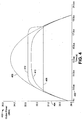
- a pulsed-waveform system such as GSM by applying a sinusoid with a magnitude of V ENV(max) on connection 146 as the V ENV signal, with V BATT ⁇ V BATT(nom) applied to connection 214. This will be explained below in FIG. 4 .
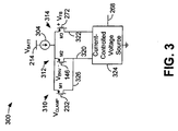
- FIG. 3 is a schematic diagram illustrating an embodiment of the invention implemented using the operational amplifier 300 of FIG. 2 .
- the operational amplifier 300 in the voltage regulator 260 includes a third input transistor 310 (PFET in this embodiment) coupled in parallel with the inverting input transistor 312 and in addition to the non-inverting input transistor 314.
- a current source 304 biases the transistors 310, 312, and 314 and is connected between V BATT 214 and the source terminals of transistors 310, 312 and 314.
- the drain terminal of transistor 310 is coupled via connection 326 to connection 320
- the drain terminal of transistor 312 is coupled via connection,320 to subsequent stages of the operational amplifier (300 of FIG. 2 ), modeled by a current controlled voltage source 324.
- the drain terminal 322 of transistor 314 is coupled to the current controlled voltage source 324.
- the output of the current controlled voltage source 324 is the output 268 which is supplied to the gate terminal of the transistor 262 of FIG. 2 .
- the gate terminal 232 of transistor 310 is connected to the reference voltage V CLAMP
- the gate terminal 146 of transistor 312 is connected to V ENV
- the gate terminal 272 of transistor 314 is connected to the output V FB of the feedback network 270 ( FIG. 2 ).
- the additional input transistor 310 is controlled by the voltage V CLAMP to provide a soft switching function when the battery voltage V BATT drops below the value V BATT(nom) .
- the output of the voltage regulator 260 is limited in accordance with an embodiment of the invention to maintain the output signal of the power amplifier on connection 156 from making an abrupt transition. If a hard limit is placed on the output of the voltage regulator 260, the limit level is preferably set sufficiently low to avoid the non-regulating region, as shown by curve 408, or an abrupt transition will occur, generating undesirable spectral regrowth. By setting the limit of the voltage regulator 260 sufficiently low to avoid operating the power amplifier 180 in the non-regulating region, the attainable output power is further reduced. Some reduction in output power is unavoidable when V BATT is reduced below V CC(nom) , as shown by curve 412, adversely affecting the allowable transmission distance and power added efficiency of the portable device.
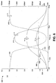
- FIG. 6 is a graphical diagram 600 illustrating the relationship of the various voltages and the drain currents of transistors 310 and 312 of FIG. 3 .
- the horizontal axis 602 represents time(s), the left hand vertical axis 604 represents voltage (V) and the right hand vertical axis 605 represents current (A).
- the curve 606 represents the voltage V CLAMP , the curve 608 represents the voltage V CC , the curve 612 represents the voltage V ENV , the curve 614 represents the drain current of the transistor 310, and the curve 616 represents the drain current of the transistor 312.
- the curves 606, 608 and 612 refer to the left hand vertical axis 604 and the curves 614 and 616 refer to the right hand vertical axis 605.
- V CLAMP is set at a level greater than V ENV(MAX) , so the current through transistor 310 (curve 614) is minimal compared to the current through transistor 312 (curve 616). However as V BATT drops, V CLAMP also drops, eventually to a level below V ENV(MAX) .
- V ENV > V CLAMP the current flowing through transistor 312 is diverted to transistor 310, so excursions of V ENV above V CLAMP result in little to no change in the current output through connection 320 ( FIG. 3 ) to the following stages of the operational amplifier 300, modeled by the current-controlled voltage source 324.
- V ENV When V ENV is reduced to a level below V CLAMP , the current is diverted back to transistor 312, so the current through connection 320 is again controlled by V ENV , and V CC on connection 168 assumes the transfer function defined by H(V ENV ). Since the current differential between transistors 310 and 312 is dependent upon the voltage differential between V ENV and V CLAMP , the transfer of current between transistors 310 and 312 occurs gradually as V ENV , shown at 612, gradually approaches V CLAMP , shown at 606, providing the "soft" clamping characteristic.
- the voltage V CLAMP is generated using the voltage clamp reference circuit 212 as shown in FIG. 2 .
- the operational amplifier 244 and an associated feedback network 252 are used to replicate the voltage regulator 260.
- a third input PFET, not shown, is included in the operational amplifier 244 to emulate the clamp transistor 310 shown in operational amplifier 300 in FIG. 3 .
- the non-inverting input 238 of operational amplifier 244 is connected to a voltage equal to V ENV(max) , thus replicating the voltage regulator 260 at full power amplifier power.
- V DROP a constant voltage drop from V BATT , referred to as V DROP . This voltage drop is equivalent to the desired drain-source voltage V DS across the transistor 262 on connection 168, used to maintain a smooth switching response in the voltage regulator 260.
- the resultant voltage, V BATT - V DROP is connected to the non-inverting input 222 of operational amplifier 220 ( FIG. 2 ).
- the inverting input 224 of operational amplifier 220 is connected to the output of the operational amplifier 244 on connection 224.
- the clamp reference voltage V CLAMP is generated independently of the voltage regulator 260 requiring no feedback around the voltage regulator 260.
- This open-loop architecture allows the output to be clamped without affecting the bandwidth of the voltage regulator, making polar modulation in a clamped condition possible.
- an open-loop architecture provides the "soft" clamping characteristic, since a feedback loop would cause a more abrupt transition of current between transistors 310 and 312 ( FIG. 3 ), resulting in a sharper clamping profile, much like the undesirable curve 408 ( FIG. 4 ).
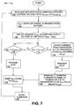
- FIG. 7 is a flow chart illustrating the operation of an embodiment of the invention.
- the blocks in the flowchart can be performed in the order shown, out of the order shown, or can be performed in parallel.
- the power amplifier module 200 is preferably designed to operate at a voltage, V BATT(nom) , to return maximum power added efficiency at a maximum designed power output.
- the baseband subsystem 110 initiates a transmit burst, ramping the voltage V ENV from a voltage V ENV(min) to a voltage V ENV(desired) , corresponding to the desired burst power.
- charge is drained from the battery and the voltage, V BATI begins to drop, forcing the voltage at node 222 ( FIG. 2 ) to drop accordingly.
- the error amplifier 220 adjusts the voltage V CLAMP to maintain the output voltage of operational amplifier 244 at the voltage V BATT - V DROP .
- V ENV is greater than V CLAMP . If, in block 712, it is determined that V ENV is greater than V CLAMP , then, in block 714, current is diverted from transistor 312 to transistor 310 ( FIG. 3 ) as V ENV exceeds V CLAMP , thus gradually limiting V CC at V BATT - V DROP . If, in block 712, it is determined that V ENV is less than V CLAMP , then, in block 716, it is determined whether V ENV is at the desired voltage V ENV(desired) .
Landscapes
- Engineering & Computer Science (AREA)
- Power Engineering (AREA)
- Amplifiers (AREA)
Claims (13)
- Verfahren zum dynamischen Regeln einer Hüllkurve und Ausgangsleistung eines Leistungsverstärkers (180), das Folgendes beinhaltet:Anlegen eines Radiofrequenz-(RF)-Signals (184) an einen Leistungsverstärker;Erzeugen eines Hüllkurvenregelsignals (146);Erzeugen eines Spannungsklemmungssignals (232);Erzeugen einer geregelten Spannung (168), wobei die geregelte Spannung auf das Hüllkurvenregelsignal bezogen ist;Anlegen der geregelten Spannung an den Leistungsverstärker;Regeln eines Ausgangs des Leistungsverstärkers gemäß der geregelten Spannung, wobei die geregelte Spannung auf das Hüllkurvenregelsignal und das Spannungsklemmungssignal anspricht;Verhindern, dass die geregelte Spannung auf ein anderes Signal als das Spannungsklemmungssignal anspricht, wenn das Hüllkurvenregelsignal einen Pegel des Spannungsklemmungssignals übersteigt; undSteuern des Übergangs der geregelten Spannung von Ansprechung auf das Hüllkurvenregelsignal auf Ansprechung auf das Spannungsklemmungssignal durch allmähliches Umstellen der geregelten Spannung zwischen Ansprechung auf das Hüllkurvenregelsignal auf Ansprechung auf das Spannungsklemmungssignal.
- Verfahren nach Anspruch 1, das ferner das Erzeugen des Spannungsklemmungssignals durch Spiegeln eines Ausgangs eines Spannungsreglers (260) beinhaltet, der zum Zuführen der geregelten Spannung konfiguriert ist.
- Verfahren nach Anspruch 1, das ferner das Steuern des Übergangs der geregelten Spannung von Ansprechung auf das Hüllkurvenregelsignal auf Ansprechung auf das Spannungsklemmungssignal beinhaltet, um Stromversorgungsumschalttransienten zu minimieren.
- Leistungsregelschaltung für einen Leistungsverstärker, die Folgendes umfasst:Mittel zum Anlegen eines Radiofrequenz-(RF)-Signals (184) an einen Leistungsverstärker;Mittel zum Erzeugen eines Hüllkurvenregelsignals (146) ;Mittel zum Erzeugen eines Spannungsklemmungssignals (232);Mittel zum Erzeugen einer geregelten Spannung (168), wobei die geregelte Spannung auf das Hüllkurvenregelsignal bezogen ist;Mittel zum Zuführen der geregelten Spannung zu dem Leistungsverstärker;Mittel zum Regeln eines Ausgangs des Leistungsverstärkers gemäß der geregelten Spannung, wobei die geregelte Spannung auf das Hüllkurvensteuersignal und das Spannungsklemmungssignal anspricht;Mittel zum Verhindern, dass die geregelte Spannung auf ein anderes Signal als das Spannungsklemmungssignal anspricht, wenn das Hüllkurvenregelsignal einen Pegel des Spannungsklemmungssignals übersteigt; undMittel zum Steuern des Übergangs der geregelten Spannung von Ansprechung auf das Hüllkurvenregelsignal auf Ansprechung auf das Spannungsklemmungssignal durch allmähliches Umstellen der geregelten Spannung von Ansprechung auf das Hüllkurvenregelsignal auf Ansprechung auf das Spannungsklemmungssignal.
- Leistungsregelschaltung nach Anspruch 4, die Mittel zum Erzeugen des Spannungsklemmungssignals durch Spiegeln eines Ausgangs eines Spannungsreglers (260) umfasst, der zum Zuführen der geregelten Spannung konfiguriert ist.
- Leistungsregelschaltung nach Anspruch 4, die Mittel zum Steuern des Übergangs der geregelten Spannung von Ansprechung auf das Hüllkurvenregelsignal auf Ansprechung auf das Spannungsklemmungssignal beinhaltet, um Stromversorgungsumschalttransienten zu minimieren.
- Leistungsregelschaltung nach Anspruch 4, die eine zum Erzeugen des Spannungsklemmungssignals konfigurierte Spannungsklemmungsreferenzschaltung und einen Spannungsregler mit einem zum Empfangen eines Hüllkurvenregelsignals konfigurierten ersten Eingang, einem zum Empfangen eines Feedback-Signals konfigurierten zweiten Eingang und einem zum Empfangen des Spannungsklemmungssignals konfigurierten dritten Eingang umfasst.
- Leistungsregelschaltung nach Anspruch 7, wobei der Spannungsregler einen ersten Operationsverstärker aufweist, wobei der erste Operationsverstärker Folgendes umfasst:einen ersten Transistor, der zum Empfangen des Hüllkurvenregelsignals konfiguriert ist, einen zweiten Transistor, der zum Empfangen des Feedback-Signals konfiguriert ist, und einen dritten Transistor, der zum Empfangen des Spannungsklemmungssignals konfiguriert ist, wobei der erste Transistor und der zweite Transistor ein erstes Eingangspaar des Operationsverstärkers bildet, wenn das Hüllkurvensignal kleiner ist als das Spannungsklemmungssignal, wobei im ersten Transistor fließender Strom zum zweiten Transistor umgeleitet wird, wenn sich das Hüllkurvensignal dem Spannungsklemmungssignal nähert, so dass der zweite Transistor und der dritte Transistor ein zweites Eingangspaar des Operationsverstärkers bilden.
- Leistungsregelschaltung nach Anspruch 8, wobei ein Übergang von einem Betriebszustand, in dem der erste Transistor und der zweite Transistor ein erstes Eingangspaar bilden, in einen Betriebszustand, in dem der zweite Transistor und der dritte Transisor ein zweites Eingangspaar bilden, allmählich ist.
- Leistungsregelschaltung nach Anspruch 9, die einen Transistor am Ausgang des Operationsverstärkers umfasst, wobei der Transistor zum Erzeugen eines geregelten Spannungssignals konfiguriert ist.
- Leistungsregelschaltung nach Anspruch 8, wobei das geregelte Spannungssignal dem Hüllkurvenregelsignal dicht folgt, bis ein gewünschtes reguliertes Spannungssignal einen Batteriespannungspegel übersteigt.
- Leistungsregelschaltung nach Anspruch 7, wobei die Spannungsklemmungsreferenzschaltung Folgendes beinhaltet:einen ersten Operationsverstärker und ein Feedback-Netzwerk, konfiguriert zum Spiegeln einer Transferfunktion und von Klemmungscharakteristiken des Spannungsreglers; undeinen zweiten Operationsverstärker, konfiguriert zum Justieren des Spannungsklemmungssignals, so dass die Ausgangsspannung des ersten Operationsverstärkers gleich VBATT - VDROP ist, wenn VBATT von einem Nennpegel abfällt, und so, dass ein Spannungsabfall (VDS) über einen Transistor an einem Ausgang des Spannungsreglers immer größer ist als VDROP, wobei VBATT die Spannung der Leistungsquelle des Leistungsverstärkers ist und VDROP ein konstanter Spannungsabfall von VBATT ist, erzeugt mit einer mit der Spannung VBATT gekoppelten, lokal erzeugten Spannungsquelle.
- Tragbarer Transceiver, der Folgendes umfasst:einen Transceiver, der ein Radiofrequenz-(RF)-Signal senden und empfangen kann; undeine Leistungsregelschaltung nach einem der Ansprüche 4 bis 12.
Applications Claiming Priority (2)
| Application Number | Priority Date | Filing Date | Title |
|---|---|---|---|
| US11/006,233 US7142053B2 (en) | 2004-12-06 | 2004-12-06 | Voltage clamp for improved transient performance of a collector voltage controlled power amplifier |
| PCT/US2005/043698 WO2006062831A2 (en) | 2004-12-06 | 2005-12-05 | Voltage clamp for improved transient performance of a collector voltage controlled power amplifier |
Publications (3)
| Publication Number | Publication Date |
|---|---|
| EP1820268A2 EP1820268A2 (de) | 2007-08-22 |
| EP1820268A4 EP1820268A4 (de) | 2009-01-21 |
| EP1820268B1 true EP1820268B1 (de) | 2016-04-06 |
Family
ID=36573534
Family Applications (1)
| Application Number | Title | Priority Date | Filing Date |
|---|---|---|---|
| EP05852811.8A Expired - Lifetime EP1820268B1 (de) | 2004-12-06 | 2005-12-05 | Spannungsklemme zur verbesserten einschwingleistung eines kollektorspannungsgesteuerten leistungsverstärkers |
Country Status (5)
| Country | Link |
|---|---|
| US (1) | US7142053B2 (de) |
| EP (1) | EP1820268B1 (de) |
| KR (1) | KR101172100B1 (de) |
| TW (1) | TWI379509B (de) |
| WO (1) | WO2006062831A2 (de) |
Families Citing this family (26)
| Publication number | Priority date | Publication date | Assignee | Title |
|---|---|---|---|---|
| US7602155B2 (en) * | 2005-07-27 | 2009-10-13 | Artesyn Technologies, Inc. | Power supply providing ultrafast modulation of output voltage |
| US7859336B2 (en) * | 2007-03-13 | 2010-12-28 | Astec International Limited | Power supply providing ultrafast modulation of output voltage |
| US7994761B2 (en) * | 2007-10-08 | 2011-08-09 | Astec International Limited | Linear regulator with RF transistors and a bias adjustment circuit |
| JP5351899B2 (ja) * | 2007-12-21 | 2013-11-27 | サンディスク テクノロジィース インコーポレイテッド | 電子機器を操作する方法、電子機器およびメモリ装置 |
| US8022770B1 (en) * | 2010-05-27 | 2011-09-20 | Skyworks Solutions, Inc. | System and method for preventing power amplifier supply voltage saturation |
| KR20120050262A (ko) * | 2010-11-10 | 2012-05-18 | 삼성전자주식회사 | 소스 팔로워 타입 전압 모드 전송기 및 그에 따른 구동 전압 제어방법 |
| JP5621649B2 (ja) | 2011-02-18 | 2014-11-12 | 富士通株式会社 | 送信装置 |
| KR101767577B1 (ko) | 2012-02-09 | 2017-08-23 | 스카이워크스 솔루션즈, 인코포레이티드 | 포락선 추적을 위한 장치 및 방법 |
| US9530719B2 (en) | 2014-06-13 | 2016-12-27 | Skyworks Solutions, Inc. | Direct die solder of gallium arsenide integrated circuit dies and methods of manufacturing gallium arsenide wafers |
| US9445371B2 (en) * | 2014-08-13 | 2016-09-13 | Skyworks Solutions, Inc. | Apparatus and methods for wideband envelope tracking systems |
| US10103693B2 (en) | 2015-09-30 | 2018-10-16 | Skyworks Solutions, Inc. | Power amplifier linearization system and method |
| US10270394B2 (en) | 2015-12-30 | 2019-04-23 | Skyworks Solutions, Inc. | Automated envelope tracking system |
| US10110169B2 (en) | 2016-09-14 | 2018-10-23 | Skyworks Solutions, Inc. | Apparatus and methods for envelope tracking systems with automatic mode selection |
| US10236831B2 (en) | 2017-05-12 | 2019-03-19 | Skyworks Solutions, Inc. | Envelope trackers providing compensation for power amplifier output load variation |
| US10615757B2 (en) | 2017-06-21 | 2020-04-07 | Skyworks Solutions, Inc. | Wide bandwidth envelope trackers |
| US10516368B2 (en) | 2017-06-21 | 2019-12-24 | Skyworks Solutions, Inc. | Fast envelope tracking systems for power amplifiers |
| US10749477B2 (en) * | 2018-09-21 | 2020-08-18 | Qualcomm Incorporated | Series voltage regulation modulating power supply |
| TWI683200B (zh) * | 2018-12-21 | 2020-01-21 | 新唐科技股份有限公司 | 動態偏壓控制系統 |
| US11082021B2 (en) | 2019-03-06 | 2021-08-03 | Skyworks Solutions, Inc. | Advanced gain shaping for envelope tracking power amplifiers |
| WO2021061851A1 (en) | 2019-09-27 | 2021-04-01 | Skyworks Solutions, Inc. | Power amplifier bias modulation for low bandwidth envelope tracking |
| US11482975B2 (en) | 2020-06-05 | 2022-10-25 | Skyworks Solutions, Inc. | Power amplifiers with adaptive bias for envelope tracking applications |
| US11855595B2 (en) | 2020-06-05 | 2023-12-26 | Skyworks Solutions, Inc. | Composite cascode power amplifiers for envelope tracking applications |
| GB2599769B (en) | 2020-08-26 | 2025-05-07 | Skyworks Solutions Inc | Power amplifier modules with controllable envelope tracking noise filters |
| US12494753B2 (en) | 2021-09-14 | 2025-12-09 | Skyworks Solutions, Inc. | Apparatus and methods for detecting and clamping power of a power amplifier |
| US12620947B2 (en) | 2022-07-07 | 2026-05-05 | Skyworks Solutions, Inc. | Power amplification system for high modulation bandwidth |
| US12483213B2 (en) | 2022-09-30 | 2025-11-25 | Skyworks Solutions, Inc. | Systems and methods for pulse shaping voltage transitions in envelope tracking systems |
Family Cites Families (13)
| Publication number | Priority date | Publication date | Assignee | Title |
|---|---|---|---|---|
| US4987385A (en) * | 1989-11-22 | 1991-01-22 | Engelmann Rudolph H | High efficiency power amplifier |
| US5625893A (en) * | 1993-07-26 | 1997-04-29 | Kahn; Leonard R. | Satellite communications system with receiver distortion correction which is controlled by up-link transmission equipment |
| US5886575A (en) * | 1997-09-30 | 1999-03-23 | Motorola, Inc. | Apparatus and method for amplifying a signal |
| US6242975B1 (en) * | 1999-05-25 | 2001-06-05 | Conexant Systems, Inc. | Envelope peak and trough limiting to improve amplifier efficiency and distortion characteristics |
| WO2002005418A2 (en) * | 2000-07-12 | 2002-01-17 | Indigo Manufacturing Inc. | Power amplifier with multiple power supplies |
| US6549071B1 (en) * | 2000-09-12 | 2003-04-15 | Silicon Laboratories, Inc. | Power amplifier circuitry and method using an inductance coupled to power amplifier switching devices |
| US6982593B2 (en) * | 2003-10-23 | 2006-01-03 | Northrop Grumman Corporation | Switching amplifier architecture |
| FR2824437B1 (fr) * | 2001-05-04 | 2005-06-03 | Eads Defence & Security Ntwk | Generateur d'un signal radiofrequence module en phase ou frequence et en amplitude, et emetteur l'incorporant |
| US6445247B1 (en) * | 2001-06-01 | 2002-09-03 | Qualcomm Incorporated | Self-controlled high efficiency power amplifier |
| US7551688B2 (en) * | 2002-04-18 | 2009-06-23 | Nokia Corporation | Waveforms for envelope tracking transmitter |
| US6624712B1 (en) * | 2002-06-11 | 2003-09-23 | Motorola, Inc. | Method and apparatus for power modulating to prevent instances of clipping |
| AU2003301490A1 (en) * | 2002-10-15 | 2004-05-04 | Triquint Semiconductor, Inc. | Automatic-bias amplifier circuit |
| US7139534B2 (en) * | 2003-03-05 | 2006-11-21 | Matsushita Electric Industrial Co., Ltd. | Transmission circuit |
-
2004
- 2004-12-06 US US11/006,233 patent/US7142053B2/en not_active Expired - Lifetime
-
2005
- 2005-12-05 WO PCT/US2005/043698 patent/WO2006062831A2/en not_active Ceased
- 2005-12-05 EP EP05852811.8A patent/EP1820268B1/de not_active Expired - Lifetime
- 2005-12-05 KR KR1020077015444A patent/KR101172100B1/ko not_active Expired - Lifetime
- 2005-12-06 TW TW094142853A patent/TWI379509B/zh not_active IP Right Cessation
Also Published As
| Publication number | Publication date |
|---|---|
| TW200631310A (en) | 2006-09-01 |
| EP1820268A2 (de) | 2007-08-22 |
| EP1820268A4 (de) | 2009-01-21 |
| KR20070093088A (ko) | 2007-09-17 |
| US7142053B2 (en) | 2006-11-28 |
| US20060119425A1 (en) | 2006-06-08 |
| WO2006062831A2 (en) | 2006-06-15 |
| WO2006062831A3 (en) | 2006-11-30 |
| TWI379509B (en) | 2012-12-11 |
| KR101172100B1 (ko) | 2012-08-10 |
Similar Documents
| Publication | Publication Date | Title |
|---|---|---|
| US7142053B2 (en) | Voltage clamp for improved transient performance of a collector voltage controlled power amplifier | |
| KR101224247B1 (ko) | 전력 제어 폐루프 내의 공급 전압 제어된 전력 증폭기를위한 듀얼 전압 조정기 | |
| US7764055B2 (en) | Polar transmitter having a dynamically controlled voltage regulator and method for operating same | |
| US6670849B1 (en) | System for closed loop power control using a linear or a non-linear power amplifier | |
| EP1902525B1 (de) | Hochfrequenzsender mit polarer schleife und amplitudensteuerung mit erhöhtem dynamikumfang | |
| US6795712B1 (en) | System for allowing a TDMA/CDMA portable transceiver to operate with closed loop power control | |
| EP2055061B1 (de) | Nachbildungslinearisierter leistungsverstärker | |
| US8606311B2 (en) | Closed-loop adaptive power control for adjusting bandwidth in a mobile handset transmitter | |
| EP2055012B1 (de) | System und verfahren zur steuerung eines korrekturfeedback- leistungsverstärkers mit geringer verzögerung | |
| US7369871B2 (en) | System and method for allowing a TDMA/CDMA portable transceiver to operate with closed loop power control | |
| KR20250020404A (ko) | 신호 증폭 회로부 | |
| KR100508355B1 (ko) | 오디오 및 rf 증폭기용 공유 전원을 구비하는 휴대용무선 송수신기 | |
| US7187314B1 (en) | System for reducing amplitude digital-to-analog converter (DAC) resolution in a polar transmitter |
Legal Events
| Date | Code | Title | Description |
|---|---|---|---|
| PUAI | Public reference made under article 153(3) epc to a published international application that has entered the european phase |
Free format text: ORIGINAL CODE: 0009012 |
|
| 17P | Request for examination filed |
Effective date: 20070609 |
|
| AK | Designated contracting states |
Kind code of ref document: A2 Designated state(s): AT BE BG CH CY CZ DE DK EE ES FI FR GB GR HU IE IS IT LI LT LU LV MC NL PL PT RO SE SI SK TR |
|
| DAX | Request for extension of the european patent (deleted) | ||
| A4 | Supplementary search report drawn up and despatched |
Effective date: 20081229 |
|
| 17Q | First examination report despatched |
Effective date: 20110624 |
|
| GRAP | Despatch of communication of intention to grant a patent |
Free format text: ORIGINAL CODE: EPIDOSNIGR1 |
|
| RIC1 | Information provided on ipc code assigned before grant |
Ipc: H03F 1/14 20060101AFI20150303BHEP Ipc: H03G 3/20 20060101ALI20150303BHEP Ipc: H03F 1/02 20060101ALI20150303BHEP |
|
| INTG | Intention to grant announced |
Effective date: 20150407 |
|
| GRAP | Despatch of communication of intention to grant a patent |
Free format text: ORIGINAL CODE: EPIDOSNIGR1 |
|
| RIC1 | Information provided on ipc code assigned before grant |
Ipc: H03G 3/00 20060101ALI20150904BHEP Ipc: H03G 3/30 20060101ALI20150904BHEP Ipc: H03F 1/34 20060101ALI20150904BHEP Ipc: H03F 1/14 20060101AFI20150904BHEP Ipc: H03F 1/02 20060101ALI20150904BHEP Ipc: H03G 3/20 20060101ALI20150904BHEP |
|
| INTG | Intention to grant announced |
Effective date: 20150929 |
|
| GRAS | Grant fee paid |
Free format text: ORIGINAL CODE: EPIDOSNIGR3 |
|
| GRAA | (expected) grant |
Free format text: ORIGINAL CODE: 0009210 |
|
| AK | Designated contracting states |
Kind code of ref document: B1 Designated state(s): AT BE BG CH CY CZ DE DK EE ES FI FR GB GR HU IE IS IT LI LT LU LV MC NL PL PT RO SE SI SK TR |
|
| REG | Reference to a national code |
Ref country code: GB Ref legal event code: FG4D |
|
| REG | Reference to a national code |
Ref country code: AT Ref legal event code: REF Ref document number: 788746 Country of ref document: AT Kind code of ref document: T Effective date: 20160415 Ref country code: CH Ref legal event code: EP |
|
| REG | Reference to a national code |
Ref country code: IE Ref legal event code: FG4D |
|
| REG | Reference to a national code |
Ref country code: DE Ref legal event code: R096 Ref document number: 602005048914 Country of ref document: DE |
|
| REG | Reference to a national code |
Ref country code: LT Ref legal event code: MG4D Ref country code: NL Ref legal event code: MP Effective date: 20160406 |
|
| REG | Reference to a national code |
Ref country code: AT Ref legal event code: MK05 Ref document number: 788746 Country of ref document: AT Kind code of ref document: T Effective date: 20160406 |
|
| PG25 | Lapsed in a contracting state [announced via postgrant information from national office to epo] |
Ref country code: NL Free format text: LAPSE BECAUSE OF FAILURE TO SUBMIT A TRANSLATION OF THE DESCRIPTION OR TO PAY THE FEE WITHIN THE PRESCRIBED TIME-LIMIT Effective date: 20160406 |
|
| PG25 | Lapsed in a contracting state [announced via postgrant information from national office to epo] |
Ref country code: PL Free format text: LAPSE BECAUSE OF FAILURE TO SUBMIT A TRANSLATION OF THE DESCRIPTION OR TO PAY THE FEE WITHIN THE PRESCRIBED TIME-LIMIT Effective date: 20160406 Ref country code: IS Free format text: LAPSE BECAUSE OF FAILURE TO SUBMIT A TRANSLATION OF THE DESCRIPTION OR TO PAY THE FEE WITHIN THE PRESCRIBED TIME-LIMIT Effective date: 20160806 Ref country code: FI Free format text: LAPSE BECAUSE OF FAILURE TO SUBMIT A TRANSLATION OF THE DESCRIPTION OR TO PAY THE FEE WITHIN THE PRESCRIBED TIME-LIMIT Effective date: 20160406 Ref country code: LT Free format text: LAPSE BECAUSE OF FAILURE TO SUBMIT A TRANSLATION OF THE DESCRIPTION OR TO PAY THE FEE WITHIN THE PRESCRIBED TIME-LIMIT Effective date: 20160406 |
|
| PG25 | Lapsed in a contracting state [announced via postgrant information from national office to epo] |
Ref country code: PT Free format text: LAPSE BECAUSE OF FAILURE TO SUBMIT A TRANSLATION OF THE DESCRIPTION OR TO PAY THE FEE WITHIN THE PRESCRIBED TIME-LIMIT Effective date: 20160808 Ref country code: AT Free format text: LAPSE BECAUSE OF FAILURE TO SUBMIT A TRANSLATION OF THE DESCRIPTION OR TO PAY THE FEE WITHIN THE PRESCRIBED TIME-LIMIT Effective date: 20160406 Ref country code: SE Free format text: LAPSE BECAUSE OF FAILURE TO SUBMIT A TRANSLATION OF THE DESCRIPTION OR TO PAY THE FEE WITHIN THE PRESCRIBED TIME-LIMIT Effective date: 20160406 Ref country code: GR Free format text: LAPSE BECAUSE OF FAILURE TO SUBMIT A TRANSLATION OF THE DESCRIPTION OR TO PAY THE FEE WITHIN THE PRESCRIBED TIME-LIMIT Effective date: 20160707 Ref country code: ES Free format text: LAPSE BECAUSE OF FAILURE TO SUBMIT A TRANSLATION OF THE DESCRIPTION OR TO PAY THE FEE WITHIN THE PRESCRIBED TIME-LIMIT Effective date: 20160406 Ref country code: LV Free format text: LAPSE BECAUSE OF FAILURE TO SUBMIT A TRANSLATION OF THE DESCRIPTION OR TO PAY THE FEE WITHIN THE PRESCRIBED TIME-LIMIT Effective date: 20160406 |
|
| REG | Reference to a national code |
Ref country code: FR Ref legal event code: PLFP Year of fee payment: 12 |
|
| PG25 | Lapsed in a contracting state [announced via postgrant information from national office to epo] |
Ref country code: IT Free format text: LAPSE BECAUSE OF FAILURE TO SUBMIT A TRANSLATION OF THE DESCRIPTION OR TO PAY THE FEE WITHIN THE PRESCRIBED TIME-LIMIT Effective date: 20160406 Ref country code: BE Free format text: LAPSE BECAUSE OF FAILURE TO SUBMIT A TRANSLATION OF THE DESCRIPTION OR TO PAY THE FEE WITHIN THE PRESCRIBED TIME-LIMIT Effective date: 20160406 |
|
| REG | Reference to a national code |
Ref country code: DE Ref legal event code: R097 Ref document number: 602005048914 Country of ref document: DE |
|
| PG25 | Lapsed in a contracting state [announced via postgrant information from national office to epo] |
Ref country code: EE Free format text: LAPSE BECAUSE OF FAILURE TO SUBMIT A TRANSLATION OF THE DESCRIPTION OR TO PAY THE FEE WITHIN THE PRESCRIBED TIME-LIMIT Effective date: 20160406 Ref country code: RO Free format text: LAPSE BECAUSE OF FAILURE TO SUBMIT A TRANSLATION OF THE DESCRIPTION OR TO PAY THE FEE WITHIN THE PRESCRIBED TIME-LIMIT Effective date: 20160406 Ref country code: DK Free format text: LAPSE BECAUSE OF FAILURE TO SUBMIT A TRANSLATION OF THE DESCRIPTION OR TO PAY THE FEE WITHIN THE PRESCRIBED TIME-LIMIT Effective date: 20160406 Ref country code: SK Free format text: LAPSE BECAUSE OF FAILURE TO SUBMIT A TRANSLATION OF THE DESCRIPTION OR TO PAY THE FEE WITHIN THE PRESCRIBED TIME-LIMIT Effective date: 20160406 Ref country code: CZ Free format text: LAPSE BECAUSE OF FAILURE TO SUBMIT A TRANSLATION OF THE DESCRIPTION OR TO PAY THE FEE WITHIN THE PRESCRIBED TIME-LIMIT Effective date: 20160406 |
|
| PLBE | No opposition filed within time limit |
Free format text: ORIGINAL CODE: 0009261 |
|
| STAA | Information on the status of an ep patent application or granted ep patent |
Free format text: STATUS: NO OPPOSITION FILED WITHIN TIME LIMIT |
|
| 26N | No opposition filed |
Effective date: 20170110 |
|
| PG25 | Lapsed in a contracting state [announced via postgrant information from national office to epo] |
Ref country code: SI Free format text: LAPSE BECAUSE OF FAILURE TO SUBMIT A TRANSLATION OF THE DESCRIPTION OR TO PAY THE FEE WITHIN THE PRESCRIBED TIME-LIMIT Effective date: 20160406 |
|
| REG | Reference to a national code |
Ref country code: CH Ref legal event code: PL |
|
| PG25 | Lapsed in a contracting state [announced via postgrant information from national office to epo] |
Ref country code: MC Free format text: LAPSE BECAUSE OF FAILURE TO SUBMIT A TRANSLATION OF THE DESCRIPTION OR TO PAY THE FEE WITHIN THE PRESCRIBED TIME-LIMIT Effective date: 20160406 |
|
| REG | Reference to a national code |
Ref country code: IE Ref legal event code: MM4A |
|
| PG25 | Lapsed in a contracting state [announced via postgrant information from national office to epo] |
Ref country code: LI Free format text: LAPSE BECAUSE OF NON-PAYMENT OF DUE FEES Effective date: 20161231 Ref country code: CH Free format text: LAPSE BECAUSE OF NON-PAYMENT OF DUE FEES Effective date: 20161231 Ref country code: LU Free format text: LAPSE BECAUSE OF NON-PAYMENT OF DUE FEES Effective date: 20161205 |
|
| PG25 | Lapsed in a contracting state [announced via postgrant information from national office to epo] |
Ref country code: IE Free format text: LAPSE BECAUSE OF NON-PAYMENT OF DUE FEES Effective date: 20161205 |
|
| REG | Reference to a national code |
Ref country code: FR Ref legal event code: PLFP Year of fee payment: 13 |
|
| PG25 | Lapsed in a contracting state [announced via postgrant information from national office to epo] |
Ref country code: CY Free format text: LAPSE BECAUSE OF FAILURE TO SUBMIT A TRANSLATION OF THE DESCRIPTION OR TO PAY THE FEE WITHIN THE PRESCRIBED TIME-LIMIT Effective date: 20160406 Ref country code: HU Free format text: LAPSE BECAUSE OF FAILURE TO SUBMIT A TRANSLATION OF THE DESCRIPTION OR TO PAY THE FEE WITHIN THE PRESCRIBED TIME-LIMIT; INVALID AB INITIO Effective date: 20051205 |
|
| PG25 | Lapsed in a contracting state [announced via postgrant information from national office to epo] |
Ref country code: TR Free format text: LAPSE BECAUSE OF FAILURE TO SUBMIT A TRANSLATION OF THE DESCRIPTION OR TO PAY THE FEE WITHIN THE PRESCRIBED TIME-LIMIT Effective date: 20160406 |
|
| PG25 | Lapsed in a contracting state [announced via postgrant information from national office to epo] |
Ref country code: BG Free format text: LAPSE BECAUSE OF FAILURE TO SUBMIT A TRANSLATION OF THE DESCRIPTION OR TO PAY THE FEE WITHIN THE PRESCRIBED TIME-LIMIT Effective date: 20160406 |
|
| PGFP | Annual fee paid to national office [announced via postgrant information from national office to epo] |
Ref country code: GB Payment date: 20241227 Year of fee payment: 20 |
|
| PGFP | Annual fee paid to national office [announced via postgrant information from national office to epo] |
Ref country code: FR Payment date: 20241226 Year of fee payment: 20 |
|
| PGFP | Annual fee paid to national office [announced via postgrant information from national office to epo] |
Ref country code: DE Payment date: 20241227 Year of fee payment: 20 |
|
| REG | Reference to a national code |
Ref country code: DE Ref legal event code: R071 Ref document number: 602005048914 Country of ref document: DE |
|
| REG | Reference to a national code |
Ref country code: GB Ref legal event code: PE20 Expiry date: 20251204 |