EP1826801A2 - Plasmaanzeigevorrichtung - Google Patents
Plasmaanzeigevorrichtung Download PDFInfo
- Publication number
- EP1826801A2 EP1826801A2 EP07250784A EP07250784A EP1826801A2 EP 1826801 A2 EP1826801 A2 EP 1826801A2 EP 07250784 A EP07250784 A EP 07250784A EP 07250784 A EP07250784 A EP 07250784A EP 1826801 A2 EP1826801 A2 EP 1826801A2
- Authority
- EP
- European Patent Office
- Prior art keywords
- discharge
- display apparatus
- plasma display
- substrate
- discharge space
- Prior art date
- Legal status (The legal status is an assumption and is not a legal conclusion. Google has not performed a legal analysis and makes no representation as to the accuracy of the status listed.)
- Withdrawn
Links
Images



Classifications
-
- H—ELECTRICITY
- H01—ELECTRIC ELEMENTS
- H01J—ELECTRIC DISCHARGE TUBES OR DISCHARGE LAMPS
- H01J11/00—Gas-filled discharge tubes with alternating current induction of the discharge, e.g. alternating current plasma display panels [AC-PDP]; Gas-filled discharge tubes without any main electrode inside the vessel; Gas-filled discharge tubes with at least one main electrode outside the vessel
- H01J11/20—Constructional details
- H01J11/50—Filling, e.g. selection of gas mixture
-
- H—ELECTRICITY
- H01—ELECTRIC ELEMENTS
- H01J—ELECTRIC DISCHARGE TUBES OR DISCHARGE LAMPS
- H01J11/00—Gas-filled discharge tubes with alternating current induction of the discharge, e.g. alternating current plasma display panels [AC-PDP]; Gas-filled discharge tubes without any main electrode inside the vessel; Gas-filled discharge tubes with at least one main electrode outside the vessel
- H01J11/20—Constructional details
- H01J11/34—Vessels, containers or parts thereof, e.g. substrates
-
- H—ELECTRICITY
- H01—ELECTRIC ELEMENTS
- H01J—ELECTRIC DISCHARGE TUBES OR DISCHARGE LAMPS
- H01J11/00—Gas-filled discharge tubes with alternating current induction of the discharge, e.g. alternating current plasma display panels [AC-PDP]; Gas-filled discharge tubes without any main electrode inside the vessel; Gas-filled discharge tubes with at least one main electrode outside the vessel
- H01J11/10—AC-PDPs with at least one main electrode being out of contact with the plasma
- H01J11/16—AC-PDPs with at least one main electrode being out of contact with the plasma with main electrodes provided inside or on the side face of the spacers
-
- H—ELECTRICITY
- H01—ELECTRIC ELEMENTS
- H01J—ELECTRIC DISCHARGE TUBES OR DISCHARGE LAMPS
- H01J11/00—Gas-filled discharge tubes with alternating current induction of the discharge, e.g. alternating current plasma display panels [AC-PDP]; Gas-filled discharge tubes without any main electrode inside the vessel; Gas-filled discharge tubes with at least one main electrode outside the vessel
- H01J11/20—Constructional details
- H01J11/22—Electrodes, e.g. special shape, material or configuration
-
- H—ELECTRICITY
- H01—ELECTRIC ELEMENTS
- H01J—ELECTRIC DISCHARGE TUBES OR DISCHARGE LAMPS
- H01J11/00—Gas-filled discharge tubes with alternating current induction of the discharge, e.g. alternating current plasma display panels [AC-PDP]; Gas-filled discharge tubes without any main electrode inside the vessel; Gas-filled discharge tubes with at least one main electrode outside the vessel
- H01J11/20—Constructional details
- H01J11/34—Vessels, containers or parts thereof, e.g. substrates
- H01J11/44—Optical arrangements or shielding arrangements, e.g. filters, black matrices, light reflecting means or electromagnetic shielding means
Definitions
- the present invention relates to a plasma display apparatus. More particularly, the present invention relates to a plasma display apparatus having an extended surface where discharge occurs and operates having an expanded viewing angle.
- PDPs plasma display panels
- Large flat display devices employing PDPs may provide large screens having certain advantages, such as providing high-quality image displays, having very thin and light designs, and having relatively wide viewing angles.
- PDPs may be classified according to the discharge voltages applied to the discharge cells, such as direct current (DC) type, alternating current (AC) type, and hybrid type. PDPs may also be classified according to the configuration of the electrodes, such as facing-discharge type and surface-discharge type.
- AC-type PDPs In DC-type PDPs, all of the electrodes may be exposed to a discharge space so that charges may move directly between facing electrodes. In AC-type PDPs, at least one of the electrodes may be covered by, for example, a dielectric layer. Also, in AC-type PDPs, discharge may be generated by an electrical field of wall charges instead of direct discharge between facing electrodes. Since charges move directly between facing electrodes in DC-type PDPs, the electrodes may be severely damaged. Accordingly, in recent years, AC-type PDPs, particularly, AC surface-discharge type PDPs having three-electrode structures, have been generally employed.
- FIG. 1 illustrates a partial, exploded perspective view of a conventional AC surface-discharge type PDP having a three-electrode structure.
- the PDP 100 includes an upper substrate 101 (also referred to as front substrate 101) and a lower substrate 102 (also referred to as a rear substrate 102) opposite to the upper substrate 101.
- Address electrodes 103 are formed on the rear substrate 102 and are buried in a first dielectric layer 104. Barrier ribs 105 are arranged on the first dielectric layer 104, thereby partitioning discharge spaces. A phosphor layer 110 is formed in each of the discharge spaces.
- a second dielectric layer 109 and a protective layer 111 are also formed on the front substrate 101. In this configuration, only about 60% of the visible light is passed through the front substrate 101. Also, since the electrodes generating discharge are formed on the top sides of the discharge spaces, i.e., on an inside surface of the front substrate 101, they reduce the amount of visible light passing through the front substrate 101.
- the conventional AC surface-discharge type PDP 100 operates with reduced luminous efficiency. Additionally, when the conventional AC surface-discharge type PDP 100 displays an image for a long period of time, charged particles of a discharge gas are ion sputtered on the phosphor layers 110 due to an electrical field, so that image sticking or a permanent afterimage occurs. Furthermore, conventional flat display devices employing PDPs do not provide a wide or unrestricted viewing angle.
- the present invention is therefore directed to a plasma display apparatus that substantially overcomes one or more of the problems due to the limitations and disadvantages of the related art.
- FIG. 1 is a partial, exploded perspective view of a conventional AC surface-discharge type PDP having a three-electrode structure;
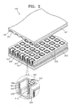
- FIG. 2 is a partial, exploded perspective view of a PDP, including an enlargement of a portion of the PDP, according to a first embodiment of the present invention
- FIG. 3A is a partial, cross-sectional view taken along the line 3A-3A illustrated in FIG. 2;
- FIG. 3B is a perspective view of discharge electrodes illustrated in FIG. 3A;
- FIG. 4 is a partial, cross-sectional view of a PDP according to a second embodiment of the present invention.
- FIGS. 5A through 5D are cross-sectional views of a process in which discharge occurs in the discharge space illustrated in FIG. 2;
- FIG. 6 is a partial, cross-sectional view of a PDP according to a third embodiment of the present invention.
- FIG. 7A is a partial, cross-sectional view of a PDP according to a fourth embodiment of the present invention.
- FIG. 7B is a perspective view of discharge electrodes illustrated in FIG. 7A.
- plasma display apparatus is intended to be interpreted broadly, and encompass PDPs and plasma display devices employing PDPs.
- FIG. 2 illustrates a partial, exploded perspective view of a PDP, including an enlargement of a portion of the PDP, according to a first embodiment of the present invention.
- the term “front” is used to denote a direction in which an image is displayed by the PDP
- the term “rear” denotes a direction opposite to the direction in which an image is displayed by the PDP.
- the PDP 200 includes a front substrate 201 and a rear substrate 202.
- the front substrate 201 and the rear substrate 202 are a predetermined distance apart from each other.
- the front substrate 201 and the rear substrate 202 face each other.
- the front substrate 201 may be made of glass or any material that is transparent.
- the PDP 200 includes a barrier structure 205.
- the barrier structure 205 is disposed between the front substrate 201 and the rear substrate 202.
- the barrier structure has a pattern to define a plurality of discharge spaces 220.
- the barrier structure 205 may have various patterns defining the plurality of discharge spaces 220.
- the barrier structure 205 may include an open barrier structure, such as strips, or a closed barrier structure, such as a waffle, a matrix, a delta, etc.
- the horizontal cross-sections of the discharge spaces 220 are rectangularly shaped in FIG. 2.
- the barrier structure 205 may be formed so that horizontal cross-sections of the discharge spaces include, for example, a polygonal shape (e.g., triangular, quadrilateral, pentagonal, etc.), a circular shape, an oval shape, etc.
- the barrier structure 205 serves both as an element that defines the discharge spaces 220 and a base on which discharge electrodes 206 and 207 are provided.
- the barrier structure 205 may have a variety of suitable horizontal, cross-sectional shapes.
- Address electrodes 203 facing the discharge spaces 220 are arranged in a predetermined pattern, for example, in strips, on the rear substrate 202. In an exemplary operation, a voltage is applied to the address electrodes 203 to select discharge spaces 220 where discharge is to be initiated.
- the pattern of the address electrodes 203 is not limited to the striped pattern illustrated in FIG. 2 and may vary according to the shape of the discharge spaces 220.
- the address electrodes 203 are on the rear substrate 202. In other embodiments, the address electrodes may be disposed at other suitable places, such as on the front substrate 201 or in the barrier structure 205. Depending on the arrangement of the discharge electrodes 206 and 207, the address electrodes 203 may be unnecessary. For example, the discharge electrodes 206 and 207 may be arranged in a manner where they cross each other. In other words, the discharge electrodes 206 and 207 may extend in directions that cross each other, when considered in a plan view. Thus, in an exemplary operation, a voltage may be applied to the front and rear discharge electrodes 206 and 207 so as to select the discharge spaces 220 where discharge is to be initiated. In such case, the address electrodes 203 would be unnecessary.
- a rear dielectric layer 204 is provided on the rear substrate 202 and covers the address electrodes 203.
- the barrier structure 205 is illustrated as being on the rear dielectric layer 204, other suitable arrangements are possible.
- the barrier structure 205 may be formed on the rear substrate 202, and the address electrodes 203 and the rear dielectric layer 204 may be sequentially formed on the front substrate 201 between sidewalls of the barrier structure 205.
- FIG. 3A illustrates a partial, cross-sectional view taken along the line 3A-3A illustrated in FIG. 2, and FIG. 3B illustrates a perspective view of discharge electrode 206, 207 of FIG. 3A.
- FIG. 3A illustrates arrangement of a discharge space 220 of the first embodiment of a PDP 200 according to the invention. It is to be understood that the arrangement of the discharge space 220 illustrated in FIGS. 3A and 3B may be replicated among the plurality of discharge spaces of the PDP 200 illustrated in FIG. 2. Further, it is to be understood that the discharge spaces illustrated in FIGS. 4, 6 and 7 may be replicated among the plurality of discharge spaces of the PDPs illustrated in FIGS. 4, 6 and 7.
- the front discharge electrode 207 (which may be, e.g., an X electrode) and the rear discharge electrode 206 (which may be, e.g., a Y electrode) are on the barrier structure 205.
- the front discharge electrode 207 and the rear discharge electrode 206 are aligned vertically and are located between the front and the rear substrates 201 and 202.
- the front discharge electrode 207 and the rear discharge electrode 206 are spaced apart from each other at a predetermined spacing, and are substantially parallel to each other and arranged to have rectangular (or more generally ring-shaped) elements.
- a discharge generated by an AC voltage applied to the front and the rear discharge electrodes 207 and 206 may be kept in the discharge space 220.
- Each electrode is, in the illustrated embodiment, composed of a series of rectangular elements, each of which surrounds a respective discharge cell.
- the elements defining each respective electrode are connected in a given direction, thereby defining the direction in which that particular electrode extends.
- the front discharge electrode 207 and the rear discharge electrode 206 have rectangular block shapes in this embodiment; however, they are not limited to this shape.
- the rectangular elements are one possible form of generally ring-shaped elements.
- the front and rear discharge electrodes 206 and 207 may have various other shapes, such as annular or cylindrical shapes.
- the front and rear discharge electrodes 206 and 207 may have different shapes from one another.
- the front discharge electrode 207 and the rear discharge electrode 206 are formed on the barrier structure 205. However, in other embodiments, they may be disposed elsewhere, such as formed within the barrier structure. Accordingly, the front discharge electrode 207 and the rear discharge electrode 206 may have any number of suitable shapes and may be disposed elsewhere.
- the front discharge electrode 207 and the rear discharge electrode 206 are formed around the sidewalls of the barrier structure 205, in parallel, so as to be formed of a number of ring shaped elements when considered in a plan view.
- the front discharge electrode 207 and the rear discharge electrode 206 are separated by a distance such that discharge generated by the application of, for example, an AC voltage, may be maintained.
- the distance between the front and rear discharge electrodes 206 and 207 is shortened as much as possible in order to operate the PDP 200 with a low driving voltage.
- front discharge electrode 207 and the rear discharge electrode 206 may be arranged differently, and may have different shapes, it may be preferable to arrange them so that discharge can easily be initiated even when a low driving voltage is applied and that the discharge can easily spread in the discharge space 220.
- the front discharge electrode 207 and the rear discharge electrode 206 are arranged so as to be insulated from each other.
- a lateral dielectric layer 208 is provided in this embodiment between the front discharge electrode 207 and the rear discharge electrode 206.
- the lateral dielectric layer 208 is provided on the barrier structure 205 and covers the front and rear discharge electrodes 207 and 206.
- a scattering field 240 (scattering element) for scattering visible light is arranged on an inside surface of the front substrate 201 that faces the discharge space 220.
- the scattering field 240 has a predetermined curvature, with a concave shape in this embodiment. That is, the scattering field 240 has a surface facing the discharge space 220 that is concave.
- the curvature of the scattering field 240 is determined in consideration of the angles at which visible light emitted from the discharge space 220 are to be scattered.
- the scattering field 240 has a rough surface in this embodiment, though embodiments of the invention are not limited in this way.
- the scattering field 240 may be processed by one of sandblasting, chemical etching, laser processing, etc., in order to form the rough surface.
- the scattering field 240 is formed from the front substrate 201 in this embodiment. Therefore, the scattering field 240 is formed in a region of the first substrate 201 which has a reduced thickness, the profile of the reduction in thickness corresponding to the curvature of the scattering field 240.
- the scattering field 240 may be a separate layer. In other words, the scattering field 240 may be considered as a concave element that disperses visible light from the discharge space 220.
- the scattering field 240 acts in the manner of a planoconcave lens to disperse the light.
- a second phosphor layer 242 is provided on the surface of the scattering field 240.
- a layer 209 for protecting the lateral dielectric layer 208 is provided on the lateral dielectric layer 208.
- the layer 209 may be made of, for example, an MgO layer.
- a first phosphor layer 210 is provided in the discharge space 220.
- the discharge space 220 is defined by the protective layer 209, the rear dielectric layer 204, and the second phosphor layer 242.
- the first phosphor layer 210 may be on any portion of the discharge space 220; however, it is preferable to have the first phosphor layer 210 cover a bottom surface 220a of the discharge space 220 and a lower portion of lateral surfaces 220b of the discharge space 220, as illustrated in FIG. 3A.
- the first phosphor layer 210 is excited by ultraviolet light generated by discharge caused by the electrodes 206 and 207 and emits visible light.
- the discharge space 220 are filled with a discharge gas, e.g., Ne, Xe, mixture thereof, etc.
- a discharge gas e.g., Ne, Xe, mixture thereof, etc.
- the upper portion (i.e. the portion nearest the front of the display) of the discharge space 220 is enclosed by the front substrate 201.
- the front substrate of other PDPs no indium tin oxide (ITO) discharge electrodes, bus electrodes, and/or dielectric layer covering the electrodes need be provided on the front substrate 201.
- ITO indium tin oxide
- the aperture ratio of the front substrate 201 may be significantly improved, and the transmittance of visible light may be improved to approximately 90%.
- the PDP 200 may be operated with a reduced driving voltage. Further, the PDP 200 may be operated with enhanced luminous efficiency.
- FIGS. 5A through 5D illustrate a single discharge space 220, it is to be understood that like processes as discussed herein may also occur among discharge spaces 220 of like arrangement of the PDP 200 of the first embodiment.
- a discharge space 220 for emitting light is selected, and wall charges are accumulated on the rear discharge electrode 206 associated with the selected discharge space 220.
- a voltage e.g., positive voltage
- another voltage e.g., a voltage lower than the positive voltage
- wall charges are moved due to a difference between the two voltages applied. That is, wall charges are moved due to the difference in voltages between the front discharge electrode 207 and the rear discharge electrode 206.
- the moving wall charges collide with discharge gas atoms within the selected discharge space 220, and discharge is initiated.
- the discharge is likely to begin in an area between the front and the rear discharge electrodes 207 and 206, where a relatively strong electrical field is formed.
- the area between the front and rear discharge electrodes 207 and 206 is located on the lateral surfaces of the discharge space 220.
- the probability that discharge will be generated is increased as compared to other PDPs in which the area between discharge electrodes is located only on the upper surface of the discharge space.
- a strong electrical field is formed between surfaces of the front and rear discharge electrodes 207 and 206 so that the discharge spreads through the entire area of the discharge space 220. That is, the discharge begins in the ring shape on the four lateral surfaces of the discharge space 220 and then spreads to the center thereof. This is in contrast to the discharge in a conventional arrangement, where discharge begins from only an upper surface of the discharge space and then spreads to the center thereof.
- the discharge that occurs in the PDP 200 of embodiments of the present invention may spread in a significantly wider range than that of the discharge that may occur in a conventional PDP.
- plasma is produced in the ring shape on the four lateral surfaces of the discharge space 220 due to the discharge and spreads to the center thereof.
- the volume of the plasma is significantly increased, and the amount of visible light generated is significantly enhanced.
- the plasma collects at the center of the discharge space 220
- spatial charges may be utilized so that the PDP may be operated with a low driving voltage and improved luminous efficiency.
- wall charges are collected at the center of the discharge space 220, which may prevent ion sputtering of the first phosphor layer 210.
- the discharge spreading in the center of the discharge space 220 generates ultraviolet light. The generated ultraviolet light excites the first phosphor layer 210 which thus generates visible light.
- the generated visible light passes through the front substrate 201.
- a portion of the visible light that is generated by the first phosphor layer 210 that is on the rear dielectric layer 204 propagates through the depth of the discharge space 220 so as to be emitted through the front substrate 201.
- a remaining portion of the visible light may not be emitted because a depth of the discharge space may be, e.g., equal to or greater than about 200 micrometers, and a height of the first phosphor layer may be, e.g., equal to or greater than about 30 micrometers. That is, an efficiency of visible light emitted through the front substrate may be poor in such arrangements. Hence, such arrangements suffer from a problem of poor efficiency of emission of visible light.
- embodiments of the invention are provided with a scattering field 240 with a predetermined curvature that faces the discharge space 220. Accordingly, the visible light indicated by the arrow within the discharge space 220 is scattered by the scattering field 240 and emitted through the front substrate 201.
- the visible light is emitted at a viewing angle ( ⁇ ).
- the viewing angle ( ⁇ ) corresponds to the predetermined curvature of the scattering field 240.
- the viewing angle of the visible light is significantly widened as compared to PDP arrangements where no scattering field 240 is provided.
- the discharge when the difference between the voltages of the front and rear discharge electrodes 207 and 206 becomes lower than a discharge voltage, the discharge may no longer be generated. Accordingly, spatial charges and wall charges are formed within the discharge space 220. To counteract this occurrence, the polarities of the voltages applied to the front and rear discharge electrodes 207 and 206 are changed so that initial discharge may be re-generated with the assistance of the wall charges. Thereafter, as illustrated in FIGS. 5A through 5C, the discharge spreads through the entire area of the discharge space 220.
- the initial discharge process may be repeated again.
- the discharge may be generated in a stable manner in the discharge space 220.
- an AC voltage is respectively applied to the front and rear discharge electrodes 207 and 206. It is to be understood, however, embodiments of the present invention are not limited to this type of discharge voltage. Additionally, embodiments of the present invention are not limited to this type of discharge, but various other types of discharge within the range understandable by one of ordinary skill in the art to which the present invention pertains may be generated in the present invention.
- FIG. 4 illustrates a partial, cross-sectional view of a PDP according to a second embodiment of the present invention. Elements of FIG. 3A indicated by reference numerals between 200 and 299 are, in turn, indicated by reference numerals between 300 and 399 in FIG. 4. Thus, elements illustrated in FIG. 4 that arranged in the same manner as those illustrated in FIG. 3A will not be described again.
- rear discharge electrodes 306a and 306b (which may be, e.g., Y electrodes) are vertically aligned with front discharge electrode 307 (which may be, e.g., an X electrode). That is, the discharge electrode 306a is located to the front of the discharge electrode 307, and the discharge electrode 306b is located to the rear of the discharge electrode 307.
- front discharge electrode 307 which may be, e.g., an X electrode
- a first phosphor layer 310 covers a bottom surface 320a of the discharge space 320 and a lower portion of lateral surfaces 320b of the discharge space 320.
- a scattering field 340 for scattering visible light is provided on an inside surface of a front substrate 301 that faces the discharge space 320.
- the scattering field 340 has a predetermined curvature, and has a concave shape in this embodiment.
- the scattering field 340 has a rough surface in this embodiment.
- a second phosphor layer 342 is provided on the scattering field 340.
- FIG. 6 illustrates a partial, cross-section view of a PDP according to a third embodiment of the present invention.
- a front discharge electrode 407 (which may be, e.g., an X electrode) and a rear discharge electrode 406 (which may be, e.g., a Y electrode) are not on or in a barrier structure 405. Rather, the front and rear discharge electrodes 407 and 406 are disposed to the front of the barrier structure 405. That is, the front and rear discharge electrodes 407 and 406 are provided between the barrier structure 405 and a front substrate 401.
- the discharge space 420 is partially defined not only by the barrier structure 405 but also by the dielectric sidewalls 415. The dielectric sidewalls 415 are provided to the front of the barrier structure 405 and on the barrier structure 405.
- Dielectric sidewalls 415 include dielectric layers 408.
- the front and rear discharge electrodes 407 and 406 are arranged one over another and buried in the dielectric layers 408.
- Protective layers 409 are arranged on the dielectric layers 408.
- the dielectric sidewalls 415 extend from the barrier structure 405to the front substrate 401.
- the front and rear discharge electrodes 407 and 406 are spaced apart from each other at a predetermined spacing within the dielectric sidewalls 415 and are substantially parallel to each other and arranged to have a number of rectangular (or more generally ring-shaped) elements.
- Each electrode is, in the illustrated embodiment, composed of a series of rectangular elements, each of which surrounds a respective discharge cell.
- the elements defining each respective electrode are connected in a given direction, thereby defining the direction in which that particular electrode extends.
- the front and the rear discharge electrodes 407 and 408 have rectangular block shapes in this embodiment. However, embodiments of the invention are not limited to this shape.
- the address electrode 403 is buried in a rear dielectric layer 404.
- the lateral surfaces of the barrier structure 405 are coated with a first phosphor layer 410.
- the first phosphor layer 410 has the same height as a height of the barrier structure 405 and is provided on an inside surface of the rear dielectric layer 404.
- a scattering field 440 for scattering visible light is provided on an inside surface of the front substrate 401 that faces the discharge space 420.
- the scattering field 440 has a predetermined curvature, and has a concave shape in this embodiment.
- the scattering field 440 has a rough surface in this embodiment.
- a second phosphor layer 442 is provided on the scattering field 440. Therefore, the scattering field 440 is formed in a region of the first substrate 401 which has a reduced thickness, the profile of the reduced thickness corresponding to the curvature of the scattering field 440.
- the visible light when discharge occurs within the discharge space 420 and visible light is emitted through the front substrate 401, the visible light is scattered by the scattering field 440 so that a wide viewing angle ( ⁇ ) is achieved.
- FIG. 7A illustrates a partial, cross-sectional view of a PDP according to a fourth embodiment of the present invention. Address electrodes are omitted in the fourth embodiment of the PDP 500 illustrated in FIG. 7A.
- FIG. 7B illustrates a perspective view of discharge electrodes of FIG. 7A.
- a front discharge electrode 507 (which may be, e.g., an X electrode) and rear discharge electrodes 506 (which may be, e.g., Y electrodes) are not located on or in a barrier structure 505. Rather, the front and rear discharge electrodes 507 and 506 are disposed to the front of the barrier structure 505. That is, the front and rear discharge electrodes 507 and 506 are located between the barrier structure 505 and a front substrate 501.
- a discharge space 520 is partially defined not only by the barrier structure 505 but also by dielectric sidewalls 515. The dielectric sidewalls 515 are located to the front of the barrier structure 505 and on the barrier structure 505.
- the dielectric sidewalls 515 include dielectric layers 508.
- the front and rear discharge electrodes 507 and 506 are arranged so that the front discharge electrode 507 is to the front of the rear discharge electrodes 506.
- the front and rear discharge electrodes 507 and 506 are buried in the dielectric layers 508.
- Protective layers 509 may cover the dielectric layers 508.
- the dielectric sidewalls 515 extend from the barrier structure 505. to the front substrate 501.
- the front discharge electrodes 507 are spaced apart from one another at regular intervals within the dielectric sidewalls 515 and extend and cross the rear discharge electrodes 506 which may extend as well. Hence, a discharge space 520 where discharge is to occur can be selected without address electrodes.
- the lateral surfaces of the barrier structure 505 are coated with a first phosphor layer 510.
- the first phosphor layer 510 has the same height as a height of the barrier structure 505 and is on the upper surface of the rear substrate 502.
- a scattering field 540 for scattering visible light is provided on an inside surface of the front substrate 501 that faces the discharge space 520.
- the scattering field 540 has a predetermined curvature and in this embodiment has a concave shape.
- the scattering field 540 has a rough surface in this embodiment.
- a second phosphor layer 542 is provided on the scattering field 540.
- the visible light when discharge occurs within the discharge space 520 and visible light is emitted through the front substrate 501, the visible light is scattered by the scattering field 540, so that a wide viewing angle ( ⁇ ) is achieved.
- a PDP according to embodiments of the present invention offer a variety of advantages. Since scattering fields are provided on a front substrate, visible light passes through the front substrate in an expanded, i.e. dispersed, fashion. Thus, a viewing angle of the PDP is significantly widened. Also, since the visible light passing through the scattering fields provides a wider viewing angle, any difference of visible light emitted from adjacent discharge spaces may be significantly reduced. Accordingly, the plasma display apparatus of the present invention provides an enhanced color display.
- an aperture ratio of the front substrate and the transmittance of visible light may be significantly increased.
- an area of a discharge space where discharge initiates and occurs may be significantly increased.
- plasma may be collected at the center of the discharge space, and luminous efficiency may be significantly improved.
- a highly concentrated gas such as Xe gas
- the PDP may be operated with a low driving voltage and enhanced luminous efficiency.
- the plasma display apparatus of embodiments of the present invention may respond afford enhanced response to discharge and may prevent permanent image sticking.
Landscapes
- Physics & Mathematics (AREA)
- Engineering & Computer Science (AREA)
- Plasma & Fusion (AREA)
- Electromagnetism (AREA)
- Chemical & Material Sciences (AREA)
- Materials Engineering (AREA)
- Gas-Filled Discharge Tubes (AREA)
Applications Claiming Priority (1)
| Application Number | Priority Date | Filing Date | Title |
|---|---|---|---|
| KR1020060017887A KR100795792B1 (ko) | 2006-02-23 | 2006-02-23 | 플라즈마 디스플레이 패널 및 이를 구비한 평판 표시 장치 |
Publications (2)
| Publication Number | Publication Date |
|---|---|
| EP1826801A2 true EP1826801A2 (de) | 2007-08-29 |
| EP1826801A3 EP1826801A3 (de) | 2009-11-11 |
Family
ID=38140095
Family Applications (1)
| Application Number | Title | Priority Date | Filing Date |
|---|---|---|---|
| EP07250784A Withdrawn EP1826801A3 (de) | 2006-02-23 | 2007-02-23 | Plasmaanzeigevorrichtung |
Country Status (5)
| Country | Link |
|---|---|
| US (1) | US20070194716A1 (de) |
| EP (1) | EP1826801A3 (de) |
| JP (1) | JP2007227352A (de) |
| KR (1) | KR100795792B1 (de) |
| CN (1) | CN101034650A (de) |
Families Citing this family (2)
| Publication number | Priority date | Publication date | Assignee | Title |
|---|---|---|---|---|
| KR100820370B1 (ko) * | 2007-05-02 | 2008-04-08 | (주)엠아이에프피디 | 대향 전극 구조를 갖는 면광원 장치 및 그 제조 방법 |
| KR100979946B1 (ko) * | 2008-08-12 | 2010-09-03 | 삼성에스디아이 주식회사 | 플라즈마 디스플레이 패널 |
Family Cites Families (13)
| Publication number | Priority date | Publication date | Assignee | Title |
|---|---|---|---|---|
| JPS5567740A (en) * | 1978-11-16 | 1980-05-22 | Matsushita Electric Ind Co Ltd | Screen |
| JPH0272388A (ja) * | 1988-09-07 | 1990-03-12 | Hitachi Ltd | 照明装置 |
| JP2593762B2 (ja) * | 1992-02-06 | 1997-03-26 | 株式会社ノリタケカンパニーリミテド | カラープラズマディスプレイパネル |
| US6229085B1 (en) * | 1996-03-13 | 2001-05-08 | Yukio Gotoh | Electromagnetic wave leakage attenuation filter |
| AU743423B2 (en) * | 1996-03-13 | 2002-01-24 | Fujitsu General Limited | Filter for preventing leakage of electromagnetic wave |
| US5917283A (en) * | 1996-09-30 | 1999-06-29 | Tektronix, Inc. | Plasma addressed liquid crystal display panel with integrated source of hydrogen |
| KR100479109B1 (ko) * | 1996-12-31 | 2005-06-23 | 주식회사 엘지이아이 | Ac플라즈마디스플레이패널 |
| JP3244055B2 (ja) * | 1998-07-10 | 2002-01-07 | 松下電器産業株式会社 | 反射型液晶表示装置 |
| KR100300422B1 (ko) * | 1999-02-25 | 2001-09-26 | 김순택 | 플라즈마 디스플레이 패널 |
| FR2831709A1 (fr) * | 2001-10-29 | 2003-05-02 | Thomson Licensing Sa | Dalle de panneau a plasma comprenant des moyens pour re-diffuser les rayonnements emis par les decharges |
| JP2003315784A (ja) * | 2002-04-11 | 2003-11-06 | Koninkl Philips Electronics Nv | 半透過型液晶表示装置及びその製造方法 |
| JP2005142002A (ja) * | 2003-11-06 | 2005-06-02 | Toyota Industries Corp | 照明装置及び表示装置 |
| JP4500094B2 (ja) * | 2004-04-27 | 2010-07-14 | 株式会社日立製作所 | プラズマディスプレイパネル |
-
2006
- 2006-02-23 KR KR1020060017887A patent/KR100795792B1/ko not_active Expired - Fee Related
- 2006-11-13 JP JP2006306820A patent/JP2007227352A/ja active Pending
-
2007
- 2007-02-21 US US11/708,485 patent/US20070194716A1/en not_active Abandoned
- 2007-02-23 EP EP07250784A patent/EP1826801A3/de not_active Withdrawn
- 2007-02-25 CN CNA2007100923153A patent/CN101034650A/zh active Pending
Also Published As
| Publication number | Publication date |
|---|---|
| KR100795792B1 (ko) | 2008-01-21 |
| US20070194716A1 (en) | 2007-08-23 |
| JP2007227352A (ja) | 2007-09-06 |
| EP1826801A3 (de) | 2009-11-11 |
| CN101034650A (zh) | 2007-09-12 |
| KR20070087460A (ko) | 2007-08-28 |
Similar Documents
| Publication | Publication Date | Title |
|---|---|---|
| JP4027909B2 (ja) | プラズマディスプレイパネル及びこれを備えた平板表示装置 | |
| JP4155968B2 (ja) | プラズマディスプレイパネル | |
| US7425796B2 (en) | Plasma display panel and manufacturing method thereof | |
| US7196470B2 (en) | Plasma display panel having sustain electrode arrangement | |
| KR100578878B1 (ko) | 플라즈마 디스플레이 패널 | |
| EP1826801A2 (de) | Plasmaanzeigevorrichtung | |
| CN100594574C (zh) | 等离子体显示板 | |
| EP1592039A1 (de) | Plasmaanzeigetafel | |
| US7227307B2 (en) | Plasma display panel | |
| KR100612240B1 (ko) | 플라즈마 디스플레이 패널 | |
| KR100590104B1 (ko) | 플라즈마 디스플레이 패널 | |
| KR100542204B1 (ko) | 플라즈마 디스플레이 패널 | |
| KR100322083B1 (ko) | 플라즈마 디스플레이 패널 | |
| KR100560543B1 (ko) | 플라즈마 디스플레이 패널 | |
| US20060164012A1 (en) | Plasma display panel (PDP) and flat panel display including the PDP | |
| US7528546B2 (en) | Plasma display panel having improved luminous efficiency and increased discharge uniformity | |
| KR100599688B1 (ko) | 플라즈마 디스플레이 패널 | |
| KR100659094B1 (ko) | 플라즈마 디스플레이 패널 | |
| US20060087234A1 (en) | Plasma display panel | |
| KR20060068260A (ko) | 플라즈마 디스플레이 패널 | |
| JP2006261112A (ja) | プラズマディスプレイパネル | |
| JP2007073526A (ja) | プラズマディスプレイパネル及びその駆動方法 | |
| KR20050099243A (ko) | 플라즈마 디스플레이 패널 | |
| JP2005347249A (ja) | プラズマディスプレイパネル | |
| KR20060102665A (ko) | 플라즈마 디스플레이 패널 |
Legal Events
| Date | Code | Title | Description |
|---|---|---|---|
| PUAI | Public reference made under article 153(3) epc to a published international application that has entered the european phase |
Free format text: ORIGINAL CODE: 0009012 |
|
| 17P | Request for examination filed |
Effective date: 20070302 |
|
| AK | Designated contracting states |
Kind code of ref document: A2 Designated state(s): AT BE BG CH CY CZ DE DK EE ES FI FR GB GR HU IE IS IT LI LT LU LV MC NL PL PT RO SE SI SK TR |
|
| AX | Request for extension of the european patent |
Extension state: AL BA HR MK YU |
|
| PUAL | Search report despatched |
Free format text: ORIGINAL CODE: 0009013 |
|
| AK | Designated contracting states |
Kind code of ref document: A3 Designated state(s): AT BE BG CH CY CZ DE DK EE ES FI FR GB GR HU IE IS IT LI LT LU LV MC NL PL PT RO SE SI SK TR |
|
| AX | Request for extension of the european patent |
Extension state: AL BA HR MK RS |
|
| STAA | Information on the status of an ep patent application or granted ep patent |
Free format text: STATUS: THE APPLICATION HAS BEEN WITHDRAWN |
|
| 18W | Application withdrawn |
Effective date: 20091218 |