EP1830404B1 - Module semi-conducteur de puissance - Google Patents
Module semi-conducteur de puissance Download PDFInfo
- Publication number
- EP1830404B1 EP1830404B1 EP07002031A EP07002031A EP1830404B1 EP 1830404 B1 EP1830404 B1 EP 1830404B1 EP 07002031 A EP07002031 A EP 07002031A EP 07002031 A EP07002031 A EP 07002031A EP 1830404 B1 EP1830404 B1 EP 1830404B1
- Authority
- EP
- European Patent Office
- Prior art keywords
- power semiconductor
- semiconductor module
- substrate
- connection elements
- stack
- Prior art date
- Legal status (The legal status is an assumption and is not a legal conclusion. Google has not performed a legal analysis and makes no representation as to the accuracy of the status listed.)
- Not-in-force
Links
Images

Classifications
-
- H—ELECTRICITY
- H10—SEMICONDUCTOR DEVICES; ELECTRIC SOLID-STATE DEVICES NOT OTHERWISE PROVIDED FOR
- H10W—GENERIC PACKAGES, INTERCONNECTIONS, CONNECTORS OR OTHER CONSTRUCTIONAL DETAILS OF DEVICES COVERED BY CLASS H10
- H10W90/00—Package configurations
-
- E—FIXED CONSTRUCTIONS
- E05—LOCKS; KEYS; WINDOW OR DOOR FITTINGS; SAFES
- E05B—LOCKS; ACCESSORIES THEREFOR; HANDCUFFS
- E05B65/00—Locks or fastenings for special use
- E05B65/0025—Locks or fastenings for special use for glass wings
-
- E—FIXED CONSTRUCTIONS
- E05—LOCKS; KEYS; WINDOW OR DOOR FITTINGS; SAFES
- E05B—LOCKS; ACCESSORIES THEREFOR; HANDCUFFS
- E05B9/00—Lock casings or latch-mechanism casings ; Fastening locks or fasteners or parts thereof to the wing
- E05B9/08—Fastening locks or fasteners or parts thereof, e.g. the casings of latch-bolt locks or cylinder locks to the wing
-
- H—ELECTRICITY
- H10—SEMICONDUCTOR DEVICES; ELECTRIC SOLID-STATE DEVICES NOT OTHERWISE PROVIDED FOR
- H10W—GENERIC PACKAGES, INTERCONNECTIONS, CONNECTORS OR OTHER CONSTRUCTIONAL DETAILS OF DEVICES COVERED BY CLASS H10
- H10W72/00—Interconnections or connectors in packages
-
- H—ELECTRICITY
- H10—SEMICONDUCTOR DEVICES; ELECTRIC SOLID-STATE DEVICES NOT OTHERWISE PROVIDED FOR
- H10W—GENERIC PACKAGES, INTERCONNECTIONS, CONNECTORS OR OTHER CONSTRUCTIONAL DETAILS OF DEVICES COVERED BY CLASS H10
- H10W72/00—Interconnections or connectors in packages
- H10W72/50—Bond wires
- H10W72/531—Shapes of wire connectors
- H10W72/5363—Shapes of wire connectors the connected ends being wedge-shaped
-
- H—ELECTRICITY
- H10—SEMICONDUCTOR DEVICES; ELECTRIC SOLID-STATE DEVICES NOT OTHERWISE PROVIDED FOR
- H10W—GENERIC PACKAGES, INTERCONNECTIONS, CONNECTORS OR OTHER CONSTRUCTIONAL DETAILS OF DEVICES COVERED BY CLASS H10
- H10W90/00—Package configurations
- H10W90/701—Package configurations characterised by the relative positions of pads or connectors relative to package parts
- H10W90/751—Package configurations characterised by the relative positions of pads or connectors relative to package parts of bond wires
- H10W90/754—Package configurations characterised by the relative positions of pads or connectors relative to package parts of bond wires between a chip and a stacked insulating package substrate, interposer or RDL
Definitions
- the invention describes a power semiconductor module in pressure contact design for mounting on a cooling component.
- a starting point of the invention form power semiconductor modules as exemplified by DE 197 19 703 A1 are known.
- Such power semiconductor modules consist of a housing with at least one electrically insulating substrate arranged therein, preferably for direct mounting on a cooling component.
- the substrate in turn consists of an insulating body with a plurality of mutually insulated metallic interconnect tracks located thereon and power semiconductor components located thereon and connected in a circuitally correct manner to these interconnect tracks.
- the known power semiconductor modules have connection elements for external load and auxiliary connections as well as connecting elements arranged in the interior. These connecting elements for circuit-compatible connections in the interior of the power semiconductor module are usually designed as Drahtbonditatien.
- the printing device has a stable, preferably metallic, pressure element for pressure build-up, an elastic cushion element for pressure storage and a bridge element for pressure introduction on separate areas of the substrate surface.
- the bridge element is preferably designed as a plastic molded body having a surface facing the cushion element, from which a plurality of pressure fingers extend in the direction of the substrate surface.
- the substrate is pressed onto a cooling component and thus the heat transfer between the substrate and the cooling component is made permanently secure.
- the elastic cushion element serves to maintain constant pressure conditions at different thermal loads and over the entire life cycle of the power semiconductor module.
- the DE 199 03 875 A1 forms the known pressure element such that on the one hand it has a particularly advantageous ratio of weight and stability and on the other hand has electrically insulated feedthroughs.
- the pressure element is designed as a plastic molded body with an inner metal core.
- This metal core has recesses for the passage of connection elements, preferably auxiliary connection elements in spring-loaded execution.
- the plastic molding encloses these recesses such that the auxiliary connection elements are electrically insulated from the metal core by means of the plastic molding.
- printing elements which have on their surface facing the substrate a plurality of pressure fingers.
- the metal core still has a preset deflection.
- such a pressure element can provide the entire functionality of a printing device mentioned above.
- a power semiconductor module wherein the load connection elements are designed such that they run in sections closely adjacent perpendicular to the substrate surface and from there emanating contact feet, which make electrical contact with the conductor tracks and at the same time exert pressure on the substrate and thus its thermal contact make a cooling component.
- the pressure is introduced and stored by means of the prior art.
- the invention has for its object to present a power semiconductor module in Drucknapsaus entry, wherein the internal insulation of the power semiconductor module is improved and the formation of the pressure contact design is simplified.
- the inventive idea is based on an arrangement of a power semiconductor module in pressure contact design on a cooling component having at least one substrate, at least two power semiconductor components arranged thereon, for example bipolar transistors, a housing, and load and control connection elements leading to the outside.
- the substrate itself has an insulating body and on the first, the interior of the power semiconductor module facing the main surface traces with load potential.
- the substrate preferably also has at least one conductor track with control potential for driving the power semiconductor components.
- the power semiconductor module further has load connection elements each formed as a metal molded body with a contact device, a band-like portion and with a plurality of this outgoing contact feet.
- the respective ribbon-like portions are arranged parallel to the substrate surface and spaced therefrom.
- the contact feet extending from the band-like portion extend to the substrate and there form the circuit of the contacts of the load terminals. For this purpose, they preferably contact the printed conductors with load potential on the substrate, alternatively alternatively directly the power semiconductor components.
- the load connection elements form a stack, wherein in this case an elastic intermediate layer is arranged between respectively adjacent load connection elements in the region of the respective strip-like sections.
- This arrangement of a plurality of elastic intermediate layer has over the prior art with only one pressure accumulator, the advantage that the individual load connection element are not rigidly but flexibly arranged to each other and thereby the contact reliability is significantly improved.
- manufacturing tolerances in the length of the respective contact feet of the individual load connection elements are compensated for one another.
- all contact feet press with the same force on their respective contact points on the substrate or on the power semiconductor components.
- the band-like portions of the load connection elements and the contact feet are made of a sheet metal body in punch-bending technique, are connected to the contact means (404, 424, 444) and then in with elastic intermediate layer (46) a stack (4) are laminated.
- This manufacturing method has the advantage that only a few individual components are to be arranged to each other by the prefabricated stack, when assembling the power semiconductor module.
- Fig. 1 shows a section through an inventive power semiconductor module.
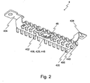
- Fig. 2 shows a three-dimensional view of a stack of load connection elements of the power semiconductor module according to the invention.
- Fig. 1 shows a section through an inventive power semiconductor module (1).
- This has a housing (3) with a frame-like housing part which is fixedly connected to the cooling member (2) of the arrangement.
- the frame-like housing part encloses the at least one substrate (5).
- This in turn has an insulating body (52), preferably an insulating ceramic, such as aluminum oxide or aluminum nitrite.
- the substrate (5) On the, the interior of the power semiconductor module (1) facing, the first main surface, the substrate (5) has a structured in itself Metallkaschtechnik.
- the individual sections of this metal lamination which is preferably configured as a copper lamination, form the printed conductors (54) of the power semiconductor module (1).
- the second main surface of the substrate (5) has a non-structured copper cladding (58) according to the prior art.
- controllable and / or uncontrolled power semiconductor devices such as IGBTs (insulated gate bipolar transistor) arranged in each case with antiparallel freewheeling diodes, or MOS-FETs. These are circuitally connected to other interconnects (54), for example by means of wire bonds (62) connected.
- the load connection elements (40, 42, 44) with the various necessary potentials serve for the external connection of the power electronic circuit in the interior of the power semiconductor module (1).
- the load connection elements (40, 42, 44) are formed as metal moldings, each having a band-like portion (402, 422, 442) parallel to the substrate surface.
- the band-like sections (402, 422, 442) form a stack (4, cf. Fig. 2 ), wherein the band-like portions of the individual load connection elements (40, 42, 44) in each case by means of an elastic intermediate layer (46) here a silicone pad spaced from each other and are electrically insulated from each other. It is particularly preferred if these silicone pads (46) are glued to the band-like sections, since thus the stack (4) is designed as a mounting unit. Necessary auxiliary connection elements are not shown for reasons of clarity in this sectional drawing.
- the power semiconductor module (1) preferably has an intermediate layer formed as an insulating molding (30) between the stack of strip-like sections (402, 422, 442) of the load connection elements (40, 42, 44) and the substrate (5).
- the insulating molding (30) has recesses (32) for passing through the contact feet (400, 420, 440) of the stack (4, cf. Fig. 2 ) on.
- the pressure device (70) for the thermal connection of the power semiconductor module (1) with a cooling component (2) and at the same time for electrically contacting the load connection elements (40, 42, 44) with the conductor tracks (54) of the substrate (5) is formed by a pressure element ( 72) for building up pressure on the stack (4, cf. Fig. 2
- the pressure element has pressure fingers (74) according to the prior art. It may also be preferred if between the pressure element (72) with flat lower side and the stack (4) a further elastic layer of the same configuration of the intermediate layer (46) is arranged.
- the pressure element (72) can furthermore be designed according to the prior art as a plastics molding with a suitable inner metal core and outer stiffening structures (76). It is also preferred if the pressure element (72) simultaneously serves as a cover of the power semiconductor module (1).
- Fig. 2 shows a three-dimensional view of a stack (4) of load connection elements (40, 42, 44) of the power semiconductor module according to the invention. Shown are the load connection elements (40, 42, 44), each having a plurality of contact feet (400, 420, 440) extending from the associated band-like portions (402, 422, 442).
- the contact devices (404, 424, 444) form the external terminals of the power semiconductor module.
- a resilient intermediate layer (46) each as a silicone pad with a minimum thickness of 1 mm.
- the respective elastic intermediate layer (46) simultaneously formed the electrical insulation of the adjacent load connection elements (40, 42, 44), as well as the pressure-transmitting and pressure-storing element of the power semiconductor module.
- load connection elements (40, 42, 44) in the region of the band-like sections (402, 422, 442) are connected to the respective intermediate layer (46) to form a mounting unit.
- This can be formed by way of example by a glued connection.
- a lamination method is used as the joining technique.
- the stack (4) further comprises recesses (406, 426, 446, 466) in the band-like sections (402, 422, 442) and the intermediate layer (46) for carrying out auxiliary connecting elements, not shown, formed as helical springs.
Landscapes
- Engineering & Computer Science (AREA)
- Mechanical Engineering (AREA)
- Cooling Or The Like Of Semiconductors Or Solid State Devices (AREA)
- Bipolar Transistors (AREA)
- Die Bonding (AREA)
Claims (7)
- Module semiconducteur de puissance (1), en configuration avec contacts par pression, destiné à être monté sur un élément refroidisseur (2), avec au moins un substrat (5), au moins deux composants semiconducteurs de puissance (60) placés dessus, un boîtier (3) et des éléments de raccordement de charge (40, 42, 44) et de commande débouchant sur l'extérieur et avec un dispositif de pression (70) destiné à appliquer une pression sur les éléments de raccordement de charge afin d'assurer leur contact électrique avec des pistes conductrices (54) du substrat, le substrat (5) présentant un corps en matière isolante (52) et portant sur sa première surface principale, tournée vers l'intérieur du module semiconducteur de puissance, lesdites pistes conductrices (54) ayant un potentiel de charge,
dans lequel les éléments de raccordement de charge sont réalisés sous la forme de corps métalliques formés avec au moins un élément de contact (404, 424), un segment en forme de ruban (402, 422, 442) et des pattes de contact (400, 420, 440) partant de ce dernier, dans lequel le segment en forme de ruban est parallèle à la surface du substrat et est écarté de celle-ci et dans lequel les pattes de contact partent du segment en forme de ruban et s'étendent jusqu'au substrat (5) et réalisent des contacts conformes au circuit, et
dans lequel les éléments de raccordement de charge (40, 42, 44) forment une pile, une couche élastique intermédiaire (46) étant disposée entre deux éléments de raccordement de charge voisins considérés, au niveau de leurs segments en forme de ruban (402, 422, 442). - Module semiconducteur de puissance (1) selon la revendication 1, dans lequel la couche élastique intermédiaire (46) prend la forme d'un coussin de silicone d'une épaisseur minimale de 1 mm.
- Module semiconducteur de puissance (1) selon la revendication 1, dans lequel la couche élastique intermédiaire (46) forme simultanément l'isolation électrique des éléments de raccordement de charge (40, 42, 44) qui lui sont adjacents.
- Module semiconducteur de puissance (1) selon la revendication 3, dans lequel les éléments de raccordement de charge (40, 42, 44), au niveau des segments en forme de ruban (402, 422, 442), sont réunis en une unité, si bien que tous les éléments de raccordement de charge sont isolés électriquement les uns par rapport aux autres, et dans lequel le dispositif de pression exerce une pression sur cette pile, si bien que les pattes de contact (400, 420, 440) sont reliées de manière électriquement conductrice aux pistes conductrices (54) du substrat (5).
- Module semiconducteur de puissance (1) selon la revendication 1, dans lequel une couche élastique supplémentaire est disposée entre la pile et un élément de pression (72) du dispositif de pression (70).
- Module semiconducteur de puissance (1) selon la revendication 1, dans lequel la pile (4) est formée par collage.
- Module semiconducteur de puissance (1) selon l'une des revendications précédentes, dans lequel le dispositif de pression (70) et la pile présentent des ouvertures (406, 426, 446, 466) destinées au passage d'éléments auxiliaires de raccordement prenant la forme de ressorts hélicoïdaux.
Applications Claiming Priority (1)
| Application Number | Priority Date | Filing Date | Title |
|---|---|---|---|
| DE102006006423A DE102006006423B4 (de) | 2006-02-13 | 2006-02-13 | Leistungshalbleitermodul und zugehöriges Herstellungsverfahren |
Publications (3)
| Publication Number | Publication Date |
|---|---|
| EP1830404A2 EP1830404A2 (fr) | 2007-09-05 |
| EP1830404A3 EP1830404A3 (fr) | 2008-05-07 |
| EP1830404B1 true EP1830404B1 (fr) | 2009-08-05 |
Family
ID=38226586
Family Applications (1)
| Application Number | Title | Priority Date | Filing Date |
|---|---|---|---|
| EP07002031A Not-in-force EP1830404B1 (fr) | 2006-02-13 | 2007-01-31 | Module semi-conducteur de puissance |
Country Status (9)
| Country | Link |
|---|---|
| US (1) | US7683472B2 (fr) |
| EP (1) | EP1830404B1 (fr) |
| JP (1) | JP5186113B2 (fr) |
| KR (1) | KR101238542B1 (fr) |
| CN (1) | CN101026146B (fr) |
| AT (1) | ATE438924T1 (fr) |
| DE (2) | DE102006006423B4 (fr) |
| DK (1) | DK1830404T3 (fr) |
| ES (1) | ES2327964T3 (fr) |
Families Citing this family (22)
| Publication number | Priority date | Publication date | Assignee | Title |
|---|---|---|---|---|
| DE102006006425B4 (de) * | 2006-02-13 | 2009-06-10 | Semikron Elektronik Gmbh & Co. Kg | Leistungshalbleitermodul in Druckkontaktausführung |
| DE102006006424B4 (de) * | 2006-02-13 | 2011-11-17 | Semikron Elektronik Gmbh & Co. Kg | Anordnung mit mindestens einem Leistungshalbleitermodul und einem Kühlbauteil und zugehöriges Herstellungsverfahren |
| DE102006052620B4 (de) * | 2006-11-08 | 2009-07-09 | Semikron Elektronik Gmbh & Co. Kg | Schaltungsanordnung mit einem Leistungsmodul, das mit einer Leiterplatte kombiniert ist. |
| DE102007003587B4 (de) | 2007-01-24 | 2009-06-10 | Semikron Elektronik Gmbh & Co. Kg | Leistungshalbleitermodul mit Druckkörper |
| DE102007044046B4 (de) * | 2007-09-14 | 2013-01-03 | Infineon Technologies Ag | Verfahren zur internen Kontaktierung eines Leistungshalbleitermoduls |
| DE102008014112A1 (de) | 2008-03-13 | 2009-10-01 | Semikron Elektronik Gmbh & Co. Kg | Leistungshalbleitermodul in Druckkontaktausführung |
| DE102008014113B4 (de) | 2008-03-13 | 2014-04-03 | Semikron Elektronik Gmbh & Co. Kg | Leistungshalbleitermodul in Druckkontaktausführung |
| CN101582414B (zh) * | 2009-04-02 | 2012-05-30 | 嘉兴斯达微电子有限公司 | 功率端子直接键合的功率模块 |
| DE102009057146B4 (de) | 2009-12-05 | 2013-09-26 | Semikron Elektronik Gmbh & Co. Kg | Druckkontaktiertes Leistungshalbleitermodul mit Hybriddruckspeicher |
| DE102009057145B4 (de) * | 2009-12-05 | 2013-12-19 | Semikron Elektronik Gmbh & Co. Kg | Druckkontaktiertes Leistungshalbleitermodul mit teilweise bandartigen Lastanschlusselementen |
| DE102011008261A1 (de) * | 2011-01-11 | 2012-07-12 | Fraunhofer-Gesellschaft zur Förderung der angewandten Forschung e.V. | Schiene für die elektrische Kontaktierung eines elektrisch leitfähigen Substrates |
| DE112015001002B4 (de) * | 2014-10-14 | 2023-08-10 | Fuji Electric Co., Ltd. | Halbleitervorrichtung |
| US9431311B1 (en) | 2015-02-19 | 2016-08-30 | Semiconductor Components Industries, Llc | Semiconductor package with elastic coupler and related methods |
| DE102016115572B4 (de) | 2016-08-23 | 2019-06-13 | Semikron Elektronik Gmbh & Co. Kg | Leistungshalbleitereinrichtungssystem mit einer ersten und einer zweiten Leistungshalbleitereinrichtung |
| WO2019053256A1 (fr) | 2017-09-15 | 2019-03-21 | Finar Module Sagl | Procédé de conditionnement et technologie d'assemblage pour un dispositif électronique |
| DE102018112552B4 (de) * | 2018-05-25 | 2021-04-15 | Semikron Elektronik Gmbh & Co. Kg | Baugruppe mit einem Kunststoffformkörper und einer Mehrzahl von Lastanschlusselementen einer Leistungshalbleitereinrichtung und Leistungshalbleitereinrichtung hiermit |
| DE102018131855A1 (de) * | 2018-12-12 | 2020-06-18 | Semikron Elektronik Gmbh & Co. Kg | Leistungshalbleitermodul mit einem Druckkörper und mit einem Druckeinleitkörper, Leistungshalbleiteranordnung hiermit sowie Leistungshalbleitersystem hiermit |
| EP3736858A1 (fr) | 2019-05-06 | 2020-11-11 | Infineon Technologies AG | Agencement de module semi-conducteur de puissance |
| EP3736855A1 (fr) * | 2019-05-06 | 2020-11-11 | Infineon Technologies AG | Agencement de module semi-conducteur de puissance et son procédé de fabrication |
| EP3736854A1 (fr) | 2019-05-06 | 2020-11-11 | Infineon Technologies AG | Agencement de module d'alimentation à semi-conducteur |
| DE102021205632A1 (de) | 2021-06-02 | 2022-12-08 | Zf Friedrichshafen Ag | Halbbrücke für einen elektrischen Antrieb eines Elektrofahrzeugs oder eines Hybridfahrzeugs, Leistungsmodul für einen Inverter und Inverter |
| WO2026058605A1 (fr) * | 2024-09-13 | 2026-03-19 | 富士電機株式会社 | Module semi-conducteur et procédé de connexion de composant externe |
Family Cites Families (20)
| Publication number | Priority date | Publication date | Assignee | Title |
|---|---|---|---|---|
| DE3232168A1 (de) * | 1982-08-30 | 1984-03-01 | Siemens AG, 1000 Berlin und 8000 München | Halbleiterbauelement mit druckkontakt |
| DE3486256T2 (de) * | 1983-09-29 | 1994-05-11 | Toshiba Kawasaki Kk | Halbleiteranordnung in Druckpackung. |
| DE4237632A1 (de) * | 1992-11-07 | 1994-05-11 | Export Contor Ausenhandelsgese | Schaltungsanordnung |
| JP3396566B2 (ja) * | 1995-10-25 | 2003-04-14 | 三菱電機株式会社 | 半導体装置 |
| DE19719703C5 (de) * | 1997-05-09 | 2005-11-17 | eupec Europäische Gesellschaft für Leistungshalbleiter mbH & Co. KG | Leistungshalbleitermodul mit Keramiksubstrat |
| DE19843309A1 (de) * | 1998-09-22 | 2000-03-23 | Asea Brown Boveri | Kurzschlussfestes IGBT Modul |
| DE19903875C2 (de) * | 1999-02-01 | 2001-11-29 | Semikron Elektronik Gmbh | Leistungshalbleiterschaltungsanordnung, insbesondere Stromumrichter, in Druckkontaktierung |
| JP2002076259A (ja) * | 2000-08-28 | 2002-03-15 | Mitsubishi Electric Corp | パワーモジュール |
| DE10121970B4 (de) * | 2001-05-05 | 2004-05-27 | Semikron Elektronik Gmbh | Leistungshalbleitermodul in Druckkontaktierung |
| DE10127947C1 (de) * | 2001-08-22 | 2002-10-17 | Semikron Elektronik Gmbh | Schaltungsanordnung |
| DE10141114C1 (de) * | 2001-06-08 | 2002-11-21 | Semikron Elektronik Gmbh | Schaltungsanordnung |
| EP1318545A1 (fr) * | 2001-12-06 | 2003-06-11 | Abb Research Ltd. | Sous-module semi-conducteur à haut prestation et module semi-conducteur à haut prestation |
| EP1367643B1 (fr) * | 2002-05-15 | 2006-04-05 | Tyco Electronics AMP GmbH | Module électronique |
| JP3669971B2 (ja) * | 2002-05-21 | 2005-07-13 | 三菱電機株式会社 | 半導体モジュール |
| US6946740B2 (en) * | 2002-07-15 | 2005-09-20 | International Rectifier Corporation | High power MCM package |
| DE102004025609B4 (de) * | 2004-05-25 | 2010-12-09 | Semikron Elektronik Gmbh & Co. Kg | Anordnung in Schraub- Druckkontaktierung mit einem Leistungshalbleitermodul |
| DE102004061936A1 (de) * | 2004-12-22 | 2006-07-06 | Siemens Ag | Anordnung eines Halbleitermoduls und einer elektrischen Verschienung |
| US7443014B2 (en) * | 2005-10-25 | 2008-10-28 | Infineon Technologies Ag | Electronic module and method of assembling the same |
| DE102006006425B4 (de) * | 2006-02-13 | 2009-06-10 | Semikron Elektronik Gmbh & Co. Kg | Leistungshalbleitermodul in Druckkontaktausführung |
| DE102006006424B4 (de) * | 2006-02-13 | 2011-11-17 | Semikron Elektronik Gmbh & Co. Kg | Anordnung mit mindestens einem Leistungshalbleitermodul und einem Kühlbauteil und zugehöriges Herstellungsverfahren |
-
2006
- 2006-02-13 DE DE102006006423A patent/DE102006006423B4/de not_active Expired - Fee Related
-
2007
- 2007-01-22 KR KR1020070006579A patent/KR101238542B1/ko not_active Expired - Fee Related
- 2007-01-31 ES ES07002031T patent/ES2327964T3/es active Active
- 2007-01-31 DE DE502007001210T patent/DE502007001210D1/de active Active
- 2007-01-31 EP EP07002031A patent/EP1830404B1/fr not_active Not-in-force
- 2007-01-31 DK DK07002031T patent/DK1830404T3/da active
- 2007-01-31 AT AT07002031T patent/ATE438924T1/de active
- 2007-02-09 JP JP2007030495A patent/JP5186113B2/ja not_active Expired - Fee Related
- 2007-02-12 CN CN2007100052665A patent/CN101026146B/zh not_active Expired - Fee Related
- 2007-02-13 US US11/705,719 patent/US7683472B2/en not_active Expired - Fee Related
Also Published As
| Publication number | Publication date |
|---|---|
| ES2327964T3 (es) | 2009-11-05 |
| CN101026146B (zh) | 2010-09-29 |
| DE102006006423B4 (de) | 2009-06-10 |
| US7683472B2 (en) | 2010-03-23 |
| EP1830404A3 (fr) | 2008-05-07 |
| DE102006006423A1 (de) | 2007-08-23 |
| DK1830404T3 (da) | 2009-11-02 |
| JP5186113B2 (ja) | 2013-04-17 |
| JP2007221127A (ja) | 2007-08-30 |
| CN101026146A (zh) | 2007-08-29 |
| ATE438924T1 (de) | 2009-08-15 |
| KR101238542B1 (ko) | 2013-02-28 |
| EP1830404A2 (fr) | 2007-09-05 |
| KR20070081743A (ko) | 2007-08-17 |
| US20070187817A1 (en) | 2007-08-16 |
| DE502007001210D1 (de) | 2009-09-17 |
Similar Documents
| Publication | Publication Date | Title |
|---|---|---|
| EP1830404B1 (fr) | Module semi-conducteur de puissance | |
| EP1843393B1 (fr) | Module de puissance semi-conducteur de type à contact par pression | |
| EP1818982B1 (fr) | Assemblage avec au moins un module semi-conducteur de puissance et un élément de refroidissement et méthode de fabrication associée | |
| EP1868243B1 (fr) | Module semi-conducteur de puissance doté d'éléments de connexion isolés électriquement les uns des autres | |
| DE102009037257B4 (de) | Leistungshalbleitermodul mit Schaltungsträger und Lastanschlusselement sowie Herstellungsverfahren hierzu | |
| EP1933379B1 (fr) | Module semi-conducteur de puissance doté de ressorts de contact | |
| EP1855319B1 (fr) | Module semi-conducteur à haute puissance | |
| DE102017109706B3 (de) | Leistungselektronische Anordnung mit Gleichspannungsverbindungselement | |
| EP1840961B1 (fr) | Module semi-conducteur de puissance | |
| EP2091080B1 (fr) | Module semi-conducteur de puissance doté d'un substrat et d'un dispositif de mise sous pression | |
| EP1950807B1 (fr) | Module semi-conducteur de puissance doté d'un corps de pression | |
| DE102005055713B4 (de) | Leistungshalbleitermodul mit Anschlusselementen | |
| EP2341535B1 (fr) | Module semi-conducteur de puissance à contact de pression doté d'un accumulateur de pression hybride | |
| EP2003693B1 (fr) | Module de convertisseur de puissance triphasé contacté par pression | |
| EP2330623A1 (fr) | Module semi-conducteur de puissance à contact de pression doté d'éléments de raccordement de charge partiellement de type bande | |
| DE102009050178B3 (de) | Leistungshalbleitermodul mit einem eine dreidimensionale Oberflächenkontur aufweisenden Substrat sowie Herstellungsverfahren hierzu | |
| DE102008014113B4 (de) | Leistungshalbleitermodul in Druckkontaktausführung |
Legal Events
| Date | Code | Title | Description |
|---|---|---|---|
| PUAI | Public reference made under article 153(3) epc to a published international application that has entered the european phase |
Free format text: ORIGINAL CODE: 0009012 |
|
| AK | Designated contracting states |
Kind code of ref document: A2 Designated state(s): AT BE BG CH CY CZ DE DK EE ES FI FR GB GR HU IE IS IT LI LT LU LV MC NL PL PT RO SE SI SK TR |
|
| AX | Request for extension of the european patent |
Extension state: AL BA HR MK YU |
|
| PUAL | Search report despatched |
Free format text: ORIGINAL CODE: 0009013 |
|
| AK | Designated contracting states |
Kind code of ref document: A3 Designated state(s): AT BE BG CH CY CZ DE DK EE ES FI FR GB GR HU IE IS IT LI LT LU LV MC NL PL PT RO SE SI SK TR |
|
| AX | Request for extension of the european patent |
Extension state: AL BA HR MK RS |
|
| 17P | Request for examination filed |
Effective date: 20080423 |
|
| 17Q | First examination report despatched |
Effective date: 20080623 |
|
| RTI1 | Title (correction) |
Free format text: POWER SEMICONDUCTOR MODULE |
|
| GRAP | Despatch of communication of intention to grant a patent |
Free format text: ORIGINAL CODE: EPIDOSNIGR1 |
|
| AKX | Designation fees paid |
Designated state(s): AT BE BG CH CY CZ DE DK EE ES FI FR GB GR HU IE IS IT LI LT LU LV MC NL PL PT RO SE SI SK TR |
|
| GRAS | Grant fee paid |
Free format text: ORIGINAL CODE: EPIDOSNIGR3 |
|
| GRAA | (expected) grant |
Free format text: ORIGINAL CODE: 0009210 |
|
| AK | Designated contracting states |
Kind code of ref document: B1 Designated state(s): AT BE BG CH CY CZ DE DK EE ES FI FR GB GR HU IE IS IT LI LT LU LV MC NL PL PT RO SE SI SK TR |
|
| REG | Reference to a national code |
Ref country code: GB Ref legal event code: FG4D Free format text: NOT ENGLISH |
|
| REG | Reference to a national code |
Ref country code: CH Ref legal event code: NV Representative=s name: BRAUNPAT BRAUN EDER AG Ref country code: CH Ref legal event code: EP |
|
| REG | Reference to a national code |
Ref country code: IE Ref legal event code: FG4D |
|
| REF | Corresponds to: |
Ref document number: 502007001210 Country of ref document: DE Date of ref document: 20090917 Kind code of ref document: P |
|
| REG | Reference to a national code |
Ref country code: DK Ref legal event code: T3 |
|
| REG | Reference to a national code |
Ref country code: ES Ref legal event code: FG2A Ref document number: 2327964 Country of ref document: ES Kind code of ref document: T3 |
|
| REG | Reference to a national code |
Ref country code: SE Ref legal event code: TRGR |
|
| REG | Reference to a national code |
Ref country code: SK Ref legal event code: T3 Ref document number: E 6118 Country of ref document: SK |
|
| LTIE | Lt: invalidation of european patent or patent extension |
Effective date: 20090805 |
|
| PG25 | Lapsed in a contracting state [announced via postgrant information from national office to epo] |
Ref country code: IS Free format text: LAPSE BECAUSE OF FAILURE TO SUBMIT A TRANSLATION OF THE DESCRIPTION OR TO PAY THE FEE WITHIN THE PRESCRIBED TIME-LIMIT Effective date: 20091205 Ref country code: LT Free format text: LAPSE BECAUSE OF FAILURE TO SUBMIT A TRANSLATION OF THE DESCRIPTION OR TO PAY THE FEE WITHIN THE PRESCRIBED TIME-LIMIT Effective date: 20090805 |
|
| PG25 | Lapsed in a contracting state [announced via postgrant information from national office to epo] |
Ref country code: PL Free format text: LAPSE BECAUSE OF FAILURE TO SUBMIT A TRANSLATION OF THE DESCRIPTION OR TO PAY THE FEE WITHIN THE PRESCRIBED TIME-LIMIT Effective date: 20090805 Ref country code: LV Free format text: LAPSE BECAUSE OF FAILURE TO SUBMIT A TRANSLATION OF THE DESCRIPTION OR TO PAY THE FEE WITHIN THE PRESCRIBED TIME-LIMIT Effective date: 20090805 Ref country code: SI Free format text: LAPSE BECAUSE OF FAILURE TO SUBMIT A TRANSLATION OF THE DESCRIPTION OR TO PAY THE FEE WITHIN THE PRESCRIBED TIME-LIMIT Effective date: 20090805 |
|
| REG | Reference to a national code |
Ref country code: IE Ref legal event code: FD4D |
|
| PG25 | Lapsed in a contracting state [announced via postgrant information from national office to epo] |
Ref country code: PT Free format text: LAPSE BECAUSE OF FAILURE TO SUBMIT A TRANSLATION OF THE DESCRIPTION OR TO PAY THE FEE WITHIN THE PRESCRIBED TIME-LIMIT Effective date: 20091205 Ref country code: BG Free format text: LAPSE BECAUSE OF FAILURE TO SUBMIT A TRANSLATION OF THE DESCRIPTION OR TO PAY THE FEE WITHIN THE PRESCRIBED TIME-LIMIT Effective date: 20091105 |
|
| PG25 | Lapsed in a contracting state [announced via postgrant information from national office to epo] |
Ref country code: EE Free format text: LAPSE BECAUSE OF FAILURE TO SUBMIT A TRANSLATION OF THE DESCRIPTION OR TO PAY THE FEE WITHIN THE PRESCRIBED TIME-LIMIT Effective date: 20090805 Ref country code: RO Free format text: LAPSE BECAUSE OF FAILURE TO SUBMIT A TRANSLATION OF THE DESCRIPTION OR TO PAY THE FEE WITHIN THE PRESCRIBED TIME-LIMIT Effective date: 20090805 Ref country code: IE Free format text: LAPSE BECAUSE OF FAILURE TO SUBMIT A TRANSLATION OF THE DESCRIPTION OR TO PAY THE FEE WITHIN THE PRESCRIBED TIME-LIMIT Effective date: 20090805 Ref country code: CZ Free format text: LAPSE BECAUSE OF FAILURE TO SUBMIT A TRANSLATION OF THE DESCRIPTION OR TO PAY THE FEE WITHIN THE PRESCRIBED TIME-LIMIT Effective date: 20090805 |
|
| PLBE | No opposition filed within time limit |
Free format text: ORIGINAL CODE: 0009261 |
|
| STAA | Information on the status of an ep patent application or granted ep patent |
Free format text: STATUS: NO OPPOSITION FILED WITHIN TIME LIMIT |
|
| 26N | No opposition filed |
Effective date: 20100507 |
|
| BERE | Be: lapsed |
Owner name: SEMIKRON ELEKTRONIK G.M.B.H. & CO. KG Effective date: 20100131 |
|
| PG25 | Lapsed in a contracting state [announced via postgrant information from national office to epo] |
Ref country code: MC Free format text: LAPSE BECAUSE OF NON-PAYMENT OF DUE FEES Effective date: 20100131 |
|
| PG25 | Lapsed in a contracting state [announced via postgrant information from national office to epo] |
Ref country code: GR Free format text: LAPSE BECAUSE OF FAILURE TO SUBMIT A TRANSLATION OF THE DESCRIPTION OR TO PAY THE FEE WITHIN THE PRESCRIBED TIME-LIMIT Effective date: 20091106 |
|
| PG25 | Lapsed in a contracting state [announced via postgrant information from national office to epo] |
Ref country code: BE Free format text: LAPSE BECAUSE OF NON-PAYMENT OF DUE FEES Effective date: 20100131 |
|
| PGRI | Patent reinstated in contracting state [announced from national office to epo] |
Ref country code: IT Effective date: 20110501 |
|
| PG25 | Lapsed in a contracting state [announced via postgrant information from national office to epo] |
Ref country code: CY Free format text: LAPSE BECAUSE OF FAILURE TO SUBMIT A TRANSLATION OF THE DESCRIPTION OR TO PAY THE FEE WITHIN THE PRESCRIBED TIME-LIMIT Effective date: 20090805 |
|
| PG25 | Lapsed in a contracting state [announced via postgrant information from national office to epo] |
Ref country code: LU Free format text: LAPSE BECAUSE OF NON-PAYMENT OF DUE FEES Effective date: 20100131 Ref country code: HU Free format text: LAPSE BECAUSE OF FAILURE TO SUBMIT A TRANSLATION OF THE DESCRIPTION OR TO PAY THE FEE WITHIN THE PRESCRIBED TIME-LIMIT Effective date: 20100206 |
|
| PG25 | Lapsed in a contracting state [announced via postgrant information from national office to epo] |
Ref country code: TR Free format text: LAPSE BECAUSE OF FAILURE TO SUBMIT A TRANSLATION OF THE DESCRIPTION OR TO PAY THE FEE WITHIN THE PRESCRIBED TIME-LIMIT Effective date: 20090805 |
|
| REG | Reference to a national code |
Ref country code: FR Ref legal event code: PLFP Year of fee payment: 10 |
|
| REG | Reference to a national code |
Ref country code: FR Ref legal event code: PLFP Year of fee payment: 11 |
|
| PGFP | Annual fee paid to national office [announced via postgrant information from national office to epo] |
Ref country code: NL Payment date: 20170124 Year of fee payment: 11 |
|
| PGFP | Annual fee paid to national office [announced via postgrant information from national office to epo] |
Ref country code: SE Payment date: 20170125 Year of fee payment: 11 Ref country code: FI Payment date: 20170120 Year of fee payment: 11 |
|
| PGFP | Annual fee paid to national office [announced via postgrant information from national office to epo] |
Ref country code: AT Payment date: 20170120 Year of fee payment: 11 Ref country code: SK Payment date: 20170124 Year of fee payment: 11 Ref country code: DK Payment date: 20170125 Year of fee payment: 11 |
|
| REG | Reference to a national code |
Ref country code: FR Ref legal event code: PLFP Year of fee payment: 12 |
|
| REG | Reference to a national code |
Ref country code: CH Ref legal event code: PCAR Free format text: NEW ADDRESS: HOLEESTRASSE 87, 4054 BASEL (CH) |
|
| REG | Reference to a national code |
Ref country code: DK Ref legal event code: EBP Effective date: 20180131 |
|
| REG | Reference to a national code |
Ref country code: NL Ref legal event code: MM Effective date: 20180201 |
|
| REG | Reference to a national code |
Ref country code: AT Ref legal event code: MM01 Ref document number: 438924 Country of ref document: AT Kind code of ref document: T Effective date: 20180131 |
|
| REG | Reference to a national code |
Ref country code: SK Ref legal event code: MM4A Ref document number: E 6118 Country of ref document: SK Effective date: 20180131 |
|
| REG | Reference to a national code |
Ref country code: SE Ref legal event code: EUG |
|
| PG25 | Lapsed in a contracting state [announced via postgrant information from national office to epo] |
Ref country code: FI Free format text: LAPSE BECAUSE OF NON-PAYMENT OF DUE FEES Effective date: 20180131 Ref country code: SE Free format text: LAPSE BECAUSE OF NON-PAYMENT OF DUE FEES Effective date: 20180201 |
|
| PG25 | Lapsed in a contracting state [announced via postgrant information from national office to epo] |
Ref country code: AT Free format text: LAPSE BECAUSE OF NON-PAYMENT OF DUE FEES Effective date: 20180131 Ref country code: SK Free format text: LAPSE BECAUSE OF NON-PAYMENT OF DUE FEES Effective date: 20180131 Ref country code: NL Free format text: LAPSE BECAUSE OF NON-PAYMENT OF DUE FEES Effective date: 20180201 |
|
| PG25 | Lapsed in a contracting state [announced via postgrant information from national office to epo] |
Ref country code: DK Free format text: LAPSE BECAUSE OF NON-PAYMENT OF DUE FEES Effective date: 20180131 |
|
| PGFP | Annual fee paid to national office [announced via postgrant information from national office to epo] |
Ref country code: CH Payment date: 20210122 Year of fee payment: 15 Ref country code: FR Payment date: 20210120 Year of fee payment: 15 Ref country code: IT Payment date: 20210129 Year of fee payment: 15 |
|
| PGFP | Annual fee paid to national office [announced via postgrant information from national office to epo] |
Ref country code: DE Payment date: 20210131 Year of fee payment: 15 Ref country code: ES Payment date: 20210217 Year of fee payment: 15 Ref country code: GB Payment date: 20210122 Year of fee payment: 15 |
|
| REG | Reference to a national code |
Ref country code: DE Ref legal event code: R119 Ref document number: 502007001210 Country of ref document: DE |
|
| REG | Reference to a national code |
Ref country code: CH Ref legal event code: PL |
|
| GBPC | Gb: european patent ceased through non-payment of renewal fee |
Effective date: 20220131 |
|
| PG25 | Lapsed in a contracting state [announced via postgrant information from national office to epo] |
Ref country code: GB Free format text: LAPSE BECAUSE OF NON-PAYMENT OF DUE FEES Effective date: 20220131 Ref country code: DE Free format text: LAPSE BECAUSE OF NON-PAYMENT OF DUE FEES Effective date: 20220802 |
|
| PG25 | Lapsed in a contracting state [announced via postgrant information from national office to epo] |
Ref country code: FR Free format text: LAPSE BECAUSE OF NON-PAYMENT OF DUE FEES Effective date: 20220131 |
|
| PG25 | Lapsed in a contracting state [announced via postgrant information from national office to epo] |
Ref country code: LI Free format text: LAPSE BECAUSE OF NON-PAYMENT OF DUE FEES Effective date: 20220131 Ref country code: CH Free format text: LAPSE BECAUSE OF NON-PAYMENT OF DUE FEES Effective date: 20220131 |
|
| REG | Reference to a national code |
Ref country code: ES Ref legal event code: FD2A Effective date: 20230303 |
|
| PG25 | Lapsed in a contracting state [announced via postgrant information from national office to epo] |
Ref country code: ES Free format text: LAPSE BECAUSE OF NON-PAYMENT OF DUE FEES Effective date: 20220201 |
|
| PG25 | Lapsed in a contracting state [announced via postgrant information from national office to epo] |
Ref country code: IT Free format text: LAPSE BECAUSE OF NON-PAYMENT OF DUE FEES Effective date: 20220131 |