EP1831920B1 - Wafer-gebondeter mos-entkopplungskondensator und herstellungsverfahren - Google Patents
Wafer-gebondeter mos-entkopplungskondensator und herstellungsverfahren Download PDFInfo
- Publication number
- EP1831920B1 EP1831920B1 EP05853565A EP05853565A EP1831920B1 EP 1831920 B1 EP1831920 B1 EP 1831920B1 EP 05853565 A EP05853565 A EP 05853565A EP 05853565 A EP05853565 A EP 05853565A EP 1831920 B1 EP1831920 B1 EP 1831920B1
- Authority
- EP
- European Patent Office
- Prior art keywords
- layer
- capacitor
- substrate
- vias
- forming
- Prior art date
- Legal status (The legal status is an assumption and is not a legal conclusion. Google has not performed a legal analysis and makes no representation as to the accuracy of the status listed.)
- Ceased
Links
Images



Classifications
-
- H—ELECTRICITY
- H10—SEMICONDUCTOR DEVICES; ELECTRIC SOLID-STATE DEVICES NOT OTHERWISE PROVIDED FOR
- H10D—INORGANIC ELECTRIC SEMICONDUCTOR DEVICES
- H10D84/00—Integrated devices formed in or on semiconductor substrates that comprise only semiconducting layers, e.g. on Si wafers or on GaAs-on-Si wafers
-
- H—ELECTRICITY
- H10—SEMICONDUCTOR DEVICES; ELECTRIC SOLID-STATE DEVICES NOT OTHERWISE PROVIDED FOR
- H10D—INORGANIC ELECTRIC SEMICONDUCTOR DEVICES
- H10D1/00—Resistors, capacitors or inductors
- H10D1/60—Capacitors
- H10D1/62—Capacitors having potential barriers
- H10D1/66—Conductor-insulator-semiconductor capacitors, e.g. MOS capacitors
-
- H—ELECTRICITY
- H10—SEMICONDUCTOR DEVICES; ELECTRIC SOLID-STATE DEVICES NOT OTHERWISE PROVIDED FOR
- H10B—ELECTRONIC MEMORY DEVICES
- H10B12/00—Dynamic random access memory [DRAM] devices
-
- H—ELECTRICITY
- H10—SEMICONDUCTOR DEVICES; ELECTRIC SOLID-STATE DEVICES NOT OTHERWISE PROVIDED FOR
- H10D—INORGANIC ELECTRIC SEMICONDUCTOR DEVICES
- H10D1/00—Resistors, capacitors or inductors
- H10D1/01—Manufacture or treatment
- H10D1/045—Manufacture or treatment of capacitors having potential barriers, e.g. varactors
- H10D1/047—Manufacture or treatment of capacitors having potential barriers, e.g. varactors of conductor-insulator-semiconductor capacitors, e.g. trench capacitors
- H10D1/048—Manufacture or treatment of capacitors having potential barriers, e.g. varactors of conductor-insulator-semiconductor capacitors, e.g. trench capacitors having PN junctions, e.g. hybrid capacitors with MOS control
-
- H—ELECTRICITY
- H10—SEMICONDUCTOR DEVICES; ELECTRIC SOLID-STATE DEVICES NOT OTHERWISE PROVIDED FOR
- H10W—GENERIC PACKAGES, INTERCONNECTIONS, CONNECTORS OR OTHER CONSTRUCTIONAL DETAILS OF DEVICES COVERED BY CLASS H10
- H10W20/00—Interconnections in chips, wafers or substrates
- H10W20/01—Manufacture or treatment
- H10W20/021—Manufacture or treatment of interconnections within wafers or substrates
- H10W20/023—Manufacture or treatment of interconnections within wafers or substrates the interconnections being through-semiconductor vias
- H10W20/0245—Manufacture or treatment of interconnections within wafers or substrates the interconnections being through-semiconductor vias comprising use of blind vias during the manufacture
-
- H—ELECTRICITY
- H10—SEMICONDUCTOR DEVICES; ELECTRIC SOLID-STATE DEVICES NOT OTHERWISE PROVIDED FOR
- H10W—GENERIC PACKAGES, INTERCONNECTIONS, CONNECTORS OR OTHER CONSTRUCTIONAL DETAILS OF DEVICES COVERED BY CLASS H10
- H10W20/00—Interconnections in chips, wafers or substrates
- H10W20/20—Interconnections within wafers or substrates, e.g. through-silicon vias [TSV]
-
- H—ELECTRICITY
- H10—SEMICONDUCTOR DEVICES; ELECTRIC SOLID-STATE DEVICES NOT OTHERWISE PROVIDED FOR
- H10W—GENERIC PACKAGES, INTERCONNECTIONS, CONNECTORS OR OTHER CONSTRUCTIONAL DETAILS OF DEVICES COVERED BY CLASS H10
- H10W20/00—Interconnections in chips, wafers or substrates
- H10W20/20—Interconnections within wafers or substrates, e.g. through-silicon vias [TSV]
- H10W20/211—Through-semiconductor vias, e.g. TSVs
- H10W20/213—Cross-sectional shapes or dispositions
- H10W20/2134—TSVs extending from the semiconductor wafer into back-end-of-line layers
-
- H—ELECTRICITY
- H10—SEMICONDUCTOR DEVICES; ELECTRIC SOLID-STATE DEVICES NOT OTHERWISE PROVIDED FOR
- H10W—GENERIC PACKAGES, INTERCONNECTIONS, CONNECTORS OR OTHER CONSTRUCTIONAL DETAILS OF DEVICES COVERED BY CLASS H10
- H10W20/00—Interconnections in chips, wafers or substrates
- H10W20/20—Interconnections within wafers or substrates, e.g. through-silicon vias [TSV]
- H10W20/211—Through-semiconductor vias, e.g. TSVs
- H10W20/218—Through-semiconductor vias, e.g. TSVs in silicon-on-insulator [SOI] wafers
-
- H—ELECTRICITY
- H10—SEMICONDUCTOR DEVICES; ELECTRIC SOLID-STATE DEVICES NOT OTHERWISE PROVIDED FOR
- H10W—GENERIC PACKAGES, INTERCONNECTIONS, CONNECTORS OR OTHER CONSTRUCTIONAL DETAILS OF DEVICES COVERED BY CLASS H10
- H10W72/00—Interconnections or connectors in packages
Definitions
- the invention relates generally to semiconductor devices, and more particularly to fashioning a metal oxide semiconductor (MOS) capacitor that can be operatively coupled to an integrated circuit to serve as a decoupling capacitor.
- MOS metal oxide semiconductor
- Capacitors such as metal oxide semiconductor (MOS) capacitors
- MOS metal oxide semiconductor
- Capacitors are often associated with integrated circuits (ICs) to facilitate the provision of a steady supply of current to one or more parts of the circuit.
- Capacitors provide a steady supply of current to ICs and mitigate transient currents by, among other things, acting as a charge reservoir that steadily discharges stored current regardless of the transients that the circuit, or parts thereof, are exposed to, such as power to ground noise, for example. Since such capacitors separate or decouple one or more parts of the IC from surrounding noise, they are often referred to as decoupling capacitors.
- MOS capacitors Although desirable, it is costly to fabricate MOS capacitors as part of ICs since doing so lengthens and complicates fabrication processes and consumes valuable semiconductor real estate, among other things, for example.
- decoupling MOS capacitors can be operatively coupled to packaging that surrounds the IC. This, however, increases the cost of packaging and moves the capacitors away from the IC, exacerbating adverse effects associated with parasitic inductance. Accordingly, it would be desirable to be able to fabricate MOS capacitors in a cost effective manner that allows the capacitors to be operatively connected to integrated circuits so that they can serve as decoupling capacitors.
- the document US 2001/0012085 is an example of an integrated circuit chip mounted on a carrier substrate via bumps, and a capacitor provided to stabilize operation of the integrated circuit chip at high frequencies
- the invention relates to forming a MOS capacitor in a cost effective manner that allows the capacitor to be operatively coupled to a portion of an integrated circuit so that the capacitor can serve as a decoupling capacitor.
- the invention discloses a method of forming the MOS decoupling capacitor as recited in claim 1, and the MOS decoupling capacitor as recited in claim 7.
- a method of forming a MOS decoupling capacitor includes patterning a layer of capacitor top electrode material that is formed over a layer of capacitor dielectric material and patterning the layer of capacitor dielectric material which is formed over a semiconductor substrate. A layer of dielectric material is formed over the substrate and the patterned layers of capacitor top electrode and dielectric materials.
- Vias are then formed within the layer of dielectric material down to the patterned layer of capacitor top electrode material and also down to the substrate. At least one deep contact via that penetrates into the substrate is also formed within the layer of dielectric material.
- the vias are filled with a conductive material, and a first metallization layer is formed over the layer of dielectric material and the filled vias.
- the first metallization layer is patterned to form conductive contact pads over the filled vias, and the capacitor is then aligned with an integrated circuit device such that the contact pads of the capacitor are aligned with contact pads of the integrated circuit device.
- An anneal is performed to fuse the contact pads of the capacitor and the contact pads of the integrated circuit device.
- Some of the substrate is then removed to expose the at least one deep contact via, and a second metallization layer is formed over the substrate and the at least one deep contact via. The second metallization layer is then patterned to form respective bond pads over the at least one deep contact via.
- the invention relates to forming a MOS capacitor that can be utilized as a decoupling capacitor.
- the capacitor is made in a cost effective manner in that it is fashioned in/on a semiconductor wafer or wafer die that matriculates through a fabrication process tailored to fabricating the capacitor. In particular, the design of the capacitor fabrication process can be tuned or optimized in terms of efficiency.
- the MOS capacitor is removed from the wafer or die and operatively coupled to a separately fabricated integrated circuit, which can then proceed for further processing, including packaging. In this manner, the decoupling capacitor can be mounted very close to the circuit device that it is to serve, which allows the capacitor to have a greater impact on the device. Additionally, coupling the capacitor to the IC according to one or more aspects of the invention does not require valuable semiconductor real estate to be sacrificed.
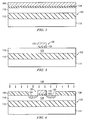
- FIG. 1 shows an example method 10 for forming a metal oxide semiconductor (MOS) decoupling capacitor according to one or more aspects of the invention.
- MOS metal oxide semiconductor
- the method 10 begins at 12 wherein a semiconductor substrate 102 is provided and a layer of capacitor dielectric material 104 is formed there-over, and a layer of capacitor top electrode material 106 is then formed over the layer of capacitor dielectric material 104 ( FIG. 2 ).
- layers 104 and 106 are substantially conformally formed. Further, it may be desirable at times to form different layers from the same or similar materials so that the layers have similar reactions to subsequent treatments (e.g., etching, CMP). At other times, however, it may be desirable to form different layers from different materials so that they respond differently to subsequent treatments (e.g., have different etch rates).
- substrate or semiconductor substrate as used herein can include a base semiconductor wafer or any portion thereof (e.g., one or more wafer die) as well as any epitaxial layers or other type of semiconductor layers formed thereover and/or associated therewith.
- the substrate can comprise, for example, silicon, SiGe, GaAs, InP and/or SOI.
- the substrate 102 comprises a silicon-on-insulator (SOI) that includes a layer of silicon material 110 overlying a thin layer of an oxide (e.g., SiO 2 ) or other insulator material 112 that overlies a bulk silicon substrate 114.
- SOI silicon-on-insulator
- layer 110 is generally formed to thickness of between about 10 nanometers to about 2 micrometers
- layer 112 is formed to a thickness of between about 100 nanometers to about 1 micrometer, for example.
- the layer of capacitor dielectric material 104 can include any of a number of suitable dielectric or non-conductive materials. Some examples include silicon dioxide, high-k dielectric materials, or a stack of such layers.
- the layer of capacitor dielectric material may include any one or more of the following, either alone or in combination: SiO 2 aluminum oxide (Al 2 O 3 ), zirconium silicate, hafnium silicate, hafnium silicon oxynitride, hafnium oxynitride, zirconium oxynitride, zirconium silicon oxynitride, hafnium silicon nitride, lanthanum oxide (La 2 O 3 ), hafnium oxide (HfO 2 ), zirconium oxide (ZrO 2 ), cerium oxide (CeO 2 ), bismuth silicon oxide (Bi 4 Si 2 O 12 ), titanium dioxide (TiO 2 ), tantalum oxide (Ta 2 O 5 ), tungsten oxide (WO 3 ), ytt
- the layer of capacitor dielectric material 104 can be formed to a thickness of about 1 nanometer or more, and can have an equivalent oxide thickness (EOT) of about 1 nanometer or less, for example, while the layer of capacitor top electrode material 106 can be formed to a thickness of between about 50 to about 200 nanometers, for example.
- the top electrode layer 106 generally includes polysilicon, SiGe and/or metal (e.g., TiN, Ta, TaN, W).
- the method 10 then advances to 14 wherein the layer of capacitor top electrode material 106 and the layer of capacitor dielectric material 104 are patterned to establish a capacitor top electrode 120 and a capacitor dielectric 122, respectively ( FIG. 3 ).
- the layer of capacitor top electrode material 106 is patterned first and the layer of capacitor dielectric material 104 becomes at least partially patterned as part of this process.
- an etchant utilized to pattern the layer of capacitor top electrode material 106 may also remove some of the layer of capacitor dielectric material 104.
- clean up steps associated with patterning the layer of capacitor top electrode material 106 as well as clean up steps associated with a hard mask removal process may also remove some of the layer of gate capacitor dielectric material 104.
- the substrate 102 may comprise an n type or a p type material (e.g., p+ or n+ ) that is electrically conductive. In such an arrangement, the substrate 102 serves as a bottom electrode 124 for the MOS capacitor 100.
- layers 104 and 106 can be patterned in any suitable manner, such as via etching and/or lithographic techniques.
- Lithography refers to processes for transferring on roe more patterns between various media.
- a radiation sensitive resist coating is formed over one or more layers to which a pattern is to be transferred.
- the resist which sometimes referred to as a photoresist, is itself first patterned by exposing it to radiation, where the radiation (selectively) passes through an intervening mask containing the pattern. As a result, the exposed or unexposed areas of the resist coating become more or less soluble, depending on the type of resist used. A developer is then used to remove the more soluble areas leaving the patterned resist.
- the pattered resist can then serve as a mask for the underlying layers which can be selectively etched to transfer the pattern thereto.
- the semiconductor substrate 102 can also be treated to establish more heavily doped regions therein.
- the method 10 advances to 16 wherein the substrate 102 can be optionally doped ( FIG. 4 ).
- a dopant material 130 can be selectively applied to areas of the substrate 102 to form more heavily doped regions 132, 134 therein.
- the dopant 130 can be selectively applied with the assistance of a layer of masking material 136 (e.g., a photoresist) that is formed over the substrate 102 and patterned.
- the dopant 130 is substantially blocked by the patterned masking material 136 and, thus, merely affects exposed regions of the substrate 102 (and optionally the capacitor top electrode 120 - depending upon the patterning of the layer of masking material 136).
- the dopant 130 alters the electrical properties of affected regions 132, 134 so that they can serve as bottom electrodes of the MOS capacitor.
- the substrate 102 can be doped with any suitable dopant 130 to instill desired electrical properties within the substrate.
- the dopant 130 may be a p type dopant that can be applied to the substrate in such a quantity and/or for such a duration that the regions 132, 134 become p+ type regions.
- Such doped regions 132, 134 generally extend to respective depths of between about 10 nanometers to about 500 nanometers, for example, in the substrate 102.
- a layer of dielectric material 140 is then formed over the substrate 102, capacitor top electrode 120 and capacitor dielectric 122 at 18 ( FIG. 5 ).
- the patterned masking material 136 is removed prior to forming the layer of dielectric material 140.
- the layer of dielectric material 140 can comprise any suitable non-conductive material(s) such as those listed above regarding the layer of capacitor dielectric material 104, and can be formed to a thickness of between about 500 nanometers to about 5 micrometers, for example.
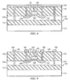
- vias are formed (e.g., etched) within the layer of dielectric material 140 ( FIG. 6 ).
- the vias can be formed by etching the layer of dielectric material 140 with the assistance of a patterned mask (e.g., a lithographically patterned photoresist).
- a patterned mask e.g., a lithographically patterned photoresist
- one via 144 is formed down to the capacitor top electrode 120
- respective vias 146, 148 are formed down to the doped regions 132 and 134
- deep contact vias 150, 152 are formed into the substrate 102 (e.g., by etching and photolithography).
- the vias facilitate forming electrical contacts down to the various areas of the capacitor 100 and substrate 102, and that any suitable number of vias can be formed according to one or more aspects of the invention.
- a single via e.g., 146 or 1428 may be formed down to the substrate 102 to allow an electrical contact to be made to this bottom electrode 124.
- deep contact vias such as vias 150, 152, are generally formed to a depth of between about 10 to about 20 micrometers, and can be made relatively large in diameter to mitigate development of unwanted resistance.
- the substrate 102 comprises an SOI
- deep contact vias such as vias 150, 152
- vias 150, 152 are formed through the layer of silicon material 110 of the substrate 102 and down into the layer of insulator material 112.
- Nitride etch stopping layers can be used, for example, where a first masking layer is employed to define the vias 144, 146, 148 to the capacitor top electrode 120 and doped regions 132, 134, respectively, and a second masking layer is employed to define the deep contact vias 150, 152.
- the vias can be formed substantially concurrently depending upon etch selectivity.
- the method 10 advances to 22 where they are filled with a conductive material 156 such as tungsten, for example ( FIG. 7 ).
- the conductive material can be added to the vias in any suitable manner, such as by chemical vapor deposition, for example.
- a layer of conductive material 160 such as copper, for example, is then formed over the dielectric layer 140 and filled vias 156 at 24 ( FIG. 8 ).
- the layer of conductive material 160 is generally formed to a thickness of between about 100 nanometers to about 1 micrometer, for example.
- the layer of conductive material 160 is then patterned over the conductive vias 156 (e.g., with etching and photolithography) to form conductive contact pads 162 over the filled vias at 26 ( FIG. 9 ).
- the contact pads 162 of the capacitor 100 are generally between about 15 by 15 square micrometers to about 100 by 100 square micrometers in size.
- the capacitor 100 is aligned (e.g., with optical and/or infrared techniques) with the particular integrated circuit device 170 for which the capacitor is to serve as a decoupling capacitor ( FIG. 10 ).
- the contact pads 162 of the capacitor 100 are aligned with contact pads 172 of the integrated circuit device 170, and an anneal is performed at 30 (e.g., at a temperature of between about 350 to about 500 degrees Celsius) to fuse the contact pads 162 of the capacitor 100 and the contact pads 172 of the integrated circuit device 170 ( FIG. 11 ).
- the capacitor 100 is generally inverted relative to the circuit device 170 to align the pads 162 and 172.
- the integrated circuit 170 can be fashioned in an area efficient manner on a semiconductor substrate while the MOS capacitor 100 can likewise be fashioned upon a semiconductor substrate in a fabrication process that is tuned to efficiently form the capacitor 100.
- the MOS capacitor 100 may be removed (e.g., cut) from a semiconductor wafer or die (e.g., upon which multiple decoupling capacitors are formed) before being annealed to the circuit device 170.
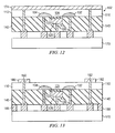
- the substrate 102 is removed to expose the one or more filled deep contact vias 150, 152 ( FIG. 11 ).
- the substrate 102 can be removed in any suitable manner, such as by back-grinding, etching, washing, etc., for example.
- back-grinding can be employed to remove the bulk silicon substrate 114 followed by a wet etch to remove the layer of insulator material 112.
- About 10 to about 15 micrometers of the filled deep contact vias 150, 152 generally remains after removing some of the substrate 102.
- a second layer of metallization 174 is then formed over the exposed surface of the substrate 102 and filled deep contact vias 150, 152 at 34 ( FIG. 12 ).
- the second layer of metallization 174 can comprise any suitable electrically conductive materials, such as aluminum, for example.
- the second layer of metallization 174 is patterned to form respective bond pads 180, 182 over at least one of the filled deep contact vias 150, 152 ( FIG. 13 ).
- the method 100 can then continue on for further processing, such as packaging of the circuit device 170 and the operatively coupled MOS decoupling capacitor 100.
- the bond pads 180, 182 e.g., bump or flip chip or wire bonds
- additional "dummy" pads can respectively be formed on the capacitor 100 and device 170 and that these pads can be fused to provide mechanically strengthening bonds 188 ( FIG. 13 ).
- One or more aspects of the invention thus allow a capacitor that can be customized for a particular application/circuit device to be produced in a cost effective manner, including reducing the cost of packaging since no additional parts or assembly are needed on the package.
- the capacitor and fabrication process can be customized and optimized, for example, in terms of cost, yield, capacitance/unit area, leakage, current, voltage, frequency, power, inductance, etc. depending upon circuit requirements, as well as the number and location of contact pads that allow the capacitor to be operatively connected to the circuit device in a stable manner.
- MOS capacitors can be made from an entire wafer, they can be made relatively large without having adverse implications on the area of the IC.
- the decoupling capacitor can thus be fabricated using a standard metal oxide semiconductor (MOS) process flow, but with the addition of a deep contact, where the capacitor can be NMOS, PMOS, NMOS in N well, or PMOS in P well.
- MOS metal oxide semiconductor
- one or more layers or structures may be described as being or containing a substance such as "tungsten”, “copper”, “silicon nitride”, etc. These description are to be understood in context and as they are used in the semiconductor manufacturing industry.
- tungsten copper
- copper copper
- silicon nitride may be a silicon rich silicon nitride or an oxygen rich silicon nitride. Silicon nitride may contain some oxygen, but not so much that the material's dielectric constant is substantially different from that of high purity stoichiometric silicon nitride.
Landscapes
- Semiconductor Integrated Circuits (AREA)
Claims (7)
- Ein Verfahren der Bildung eines MOS-Entkopplungskondensators bestehend aus :der Strukturierung einer Schicht von Kondensatoroberelektrodematerial (106, 120), das über einer Schicht von Kondensatordielektrischenmaterial (104, 122) geformt wird;der Strukturierung einer Schicht von Kondensatordielektrischenmaterial (104), das über einem Halbleitersubstrat (102) geformt wird;der Bildung einer Schicht von dielektrischen Material (140) über dem Substrat (102) und den strukturierten Schichten von Kondensatoroberelektrode (120) und dielektrischen Materialen (122);der Bildung von Durchkontaktierungen (144-152) innerhalb der Schicht von dielektrischen Material (140) bis zur strukturierten Schicht von Kondensatoroberelektrodematerial (120) und bis zum Substrat (102) einschließlich der Bildung von mindestens einer tiefen Kontaktdurchkontaktierung (150, 152), die in das Substrat (102) durchbricht;der Auffüllung der Durchkontaktierungen mit einem leitenden Material (156); Der Bildung einer ersten Metallisierungsschicht (160) über der Schicht von dielektrischen Material (140) und aufgefüllten Durchkontaktierungen (156);der Strukturierung der ersten Metallisierungsschicht, um leitenden Kontaktpads über die aufgefüllten Durchkontaktierungen (156) zu formen;dem Fluchten des Kondensators mit einem integrierten Schaltungsgerät (170), damit die Kontaktpads (162) des Kondensators mit dem Kontaktpads (172) des intergrierten Schaltungsgeräts (170) gefluchtet werden;der Ausführung von einem Ausglühen, um die Kontaktpads (172) des Kondensators und die Kontaktpads (172) des integrierten Schaltungsgeräts (170) zu fusionieren;der Abnahme von ein bisschen des Substrats (102), um die mindestens eine tiefe Kontaktdurchkontaktierung (150, 152) darzulegen;der Bildung einer zweiten Metallisierungsschicht (174) über dem Substrat (102) und die mindestens eine tiefe Kontaktdurchkontaktierung (150, 152); undder Strukturierung der zweiten Metallisierungsschicht (174), um jeweiligen Bondpads (180, 182) über der mindestens eine tiefe Kontaktdurchkontaktierung (150, 152) zu formen.
- Das Verfahren nach Anspruch 1, wobei die Abnahme von ein bisschen des Substrats aus dem Ruckseitenschleifverfahren des Substrats besteht, um die mindestens eine tiefe Kontaktdurchkontaktierung darzulegen.
- Das Verfahren nach Anspruch 2, wobei das Substrat ein SOI-Substrat ist, das aus einer Schicht von Siliziummaterial besteht, welche Schicht eine Schicht von Isolatormaterial überliegt, welches Isolatormaterial dem Massesiliziumsubstrat überliegt, wobei die mindestens eine tiefe Kontaktdurchkontaktierung durch die Schicht von Siliziummaterial und innerhalb der Schicht von Isolatormaterial durchbricht.
- Das Verfahren nach Anspruch 2, wobei das Substrat ein SOI-Substrat ist, das aus einer Schicht von Siliziummaterial besteht, welche Schicht eine Schicht von Isolatormaterial überliegt, welches Isolatormaterial dem Massesiliziumsubstrat überliegt, wobei die mindestens eine tiefe Kontaktdurchkontaktierung durch die Schicht von Siliziummaterial und innerhalb der Schicht von Isolatormaterial durchbricht, das Verfahren dazu aus der Ausführung einer Nassätzverarbeitung besteht, um die Schicht von Isolatormaterial nach dem Ruckseitenschleifverfahren des Massensiliziumsubstrats abzunehmen.
- Das Verfahren nach Ansprüchen 1-4, dazu besteht aus:selektiv dotieren die Bereichen von dem Substrat anliegend die strukturierte Kondensatoroberelektrode und Kondensatordielektrischenschichten bevor die Bildung der Schicht eines dielektrischen Materials.
- Das Verfahren von Anspruch 5, wobei mindestens eine der Durchkontakteriungen unter bis den dotierten Bereichen des Substrats geformt wird.
- Ein MOS-Entkopplungskondensator, der durch das Verfahren nach allen vorhergehenden Ansprüchen geformt wird.
Applications Claiming Priority (2)
| Application Number | Priority Date | Filing Date | Title |
|---|---|---|---|
| US11/008,007 US7064043B1 (en) | 2004-12-09 | 2004-12-09 | Wafer bonded MOS decoupling capacitor |
| PCT/US2005/044681 WO2006063259A1 (en) | 2004-12-09 | 2005-12-09 | Wafer bonded mos decoupling capacitor |
Publications (3)
| Publication Number | Publication Date |
|---|---|
| EP1831920A1 EP1831920A1 (de) | 2007-09-12 |
| EP1831920A4 EP1831920A4 (de) | 2011-07-27 |
| EP1831920B1 true EP1831920B1 (de) | 2013-02-20 |
Family
ID=36578250
Family Applications (1)
| Application Number | Title | Priority Date | Filing Date |
|---|---|---|---|
| EP05853565A Ceased EP1831920B1 (de) | 2004-12-09 | 2005-12-09 | Wafer-gebondeter mos-entkopplungskondensator und herstellungsverfahren |
Country Status (5)
| Country | Link |
|---|---|
| US (1) | US7064043B1 (de) |
| EP (1) | EP1831920B1 (de) |
| KR (1) | KR100845058B1 (de) |
| CN (1) | CN101116174B (de) |
| WO (1) | WO2006063259A1 (de) |
Families Citing this family (25)
| Publication number | Priority date | Publication date | Assignee | Title |
|---|---|---|---|---|
| JP2006059939A (ja) * | 2004-08-19 | 2006-03-02 | Fujitsu Ltd | Misキャパシタおよびmisキャパシタ作成方法 |
| US7316962B2 (en) * | 2005-01-07 | 2008-01-08 | Infineon Technologies Ag | High dielectric constant materials |
| US20060151822A1 (en) * | 2005-01-07 | 2006-07-13 | Shrinivas Govindarajan | DRAM with high K dielectric storage capacitor and method of making the same |
| KR100810487B1 (ko) * | 2005-12-08 | 2008-03-07 | 한국전자통신연구원 | 반도체 집적회로의 전원선 레이아웃 방법 및 그 방법을이용하여 제작된 반도체 집적 회로 |
| US7657859B2 (en) * | 2005-12-08 | 2010-02-02 | International Business Machines Corporation | Method for IC wiring yield optimization, including wire widening during and after routing |
| JP2007266474A (ja) * | 2006-03-29 | 2007-10-11 | Hitachi Ltd | 半導体記憶装置 |
| US7816737B2 (en) * | 2006-03-31 | 2010-10-19 | Tokyo Electron Limited | Semiconductor device with gate dielectric containing mixed rare earth elements |
| US7759746B2 (en) * | 2006-03-31 | 2010-07-20 | Tokyo Electron Limited | Semiconductor device with gate dielectric containing aluminum and mixed rare earth elements |
| US8012442B2 (en) * | 2006-03-31 | 2011-09-06 | Tokyo Electron Limited | Method of forming mixed rare earth nitride and aluminum nitride films by atomic layer deposition |
| US20070237697A1 (en) * | 2006-03-31 | 2007-10-11 | Tokyo Electron Limited | Method of forming mixed rare earth oxide and aluminate films by atomic layer deposition |
| US8097300B2 (en) * | 2006-03-31 | 2012-01-17 | Tokyo Electron Limited | Method of forming mixed rare earth oxynitride and aluminum oxynitride films by atomic layer deposition |
| US7759747B2 (en) * | 2006-08-31 | 2010-07-20 | Micron Technology, Inc. | Tantalum aluminum oxynitride high-κ dielectric |
| US20080079111A1 (en) * | 2006-09-29 | 2008-04-03 | Tokyo Electron Limited | Semiconductor devices containing nitrided high dielectric constant films |
| US7767262B2 (en) * | 2006-09-29 | 2010-08-03 | Tokyo Electron Limited | Nitrogen profile engineering in nitrided high dielectric constant films |
| US7723771B2 (en) * | 2007-03-30 | 2010-05-25 | Qimonda Ag | Zirconium oxide based capacitor and process to manufacture the same |
| KR100940660B1 (ko) | 2007-12-24 | 2010-02-05 | 주식회사 동부하이텍 | 반도체칩의 제조방법 |
| US7977799B2 (en) * | 2008-04-30 | 2011-07-12 | Avago Technologies Wireless Ip (Singapore) Pte. Ltd. | Planar packageless semiconductor structure with via and coplanar contacts |
| US8076241B2 (en) * | 2009-09-30 | 2011-12-13 | Tokyo Electron Limited | Methods for multi-step copper plating on a continuous ruthenium film in recessed features |
| US20120012979A1 (en) * | 2010-07-15 | 2012-01-19 | International Business Machines Corporation | Semiconductor capacitor |
| KR20120067525A (ko) * | 2010-12-16 | 2012-06-26 | 삼성전자주식회사 | 반도체 소자 및 이의 제조 방법 |
| US9275985B1 (en) * | 2011-07-15 | 2016-03-01 | Marvell International Ltd. | RC networks that include an integrated high resistance resistor on top of a MOS capacitor |
| JP2013115371A (ja) * | 2011-11-30 | 2013-06-10 | Sumitomo Electric Device Innovations Inc | 容量素子 |
| US9847293B1 (en) | 2016-08-18 | 2017-12-19 | Qualcomm Incorporated | Utilization of backside silicidation to form dual side contacted capacitor |
| CN109903802B (zh) * | 2017-12-11 | 2021-08-20 | 长鑫存储技术有限公司 | 一次性可编程非易失性熔丝存储单元 |
| JP2021153149A (ja) * | 2020-03-24 | 2021-09-30 | キオクシア株式会社 | 半導体装置 |
Family Cites Families (10)
| Publication number | Priority date | Publication date | Assignee | Title |
|---|---|---|---|---|
| US5256562A (en) * | 1990-12-31 | 1993-10-26 | Kopin Corporation | Method for manufacturing a semiconductor device using a circuit transfer film |
| US5756395A (en) * | 1995-08-18 | 1998-05-26 | Lsi Logic Corporation | Process for forming metal interconnect structures for use with integrated circuit devices to form integrated circuit structures |
| US6558998B2 (en) * | 1998-06-15 | 2003-05-06 | Marc Belleville | SOI type integrated circuit with a decoupling capacity and process for embodiment of such a circuit |
| US20010013660A1 (en) * | 1999-01-04 | 2001-08-16 | Peter Richard Duncombe | Beol decoupling capacitor |
| US6222246B1 (en) * | 1999-01-08 | 2001-04-24 | Intel Corporation | Flip-chip having an on-chip decoupling capacitor |
| US6316981B1 (en) * | 2000-03-13 | 2001-11-13 | Intel Corporation | Signal distribution network on backside of substrate |
| US6806568B2 (en) * | 2001-07-20 | 2004-10-19 | The Board Of Trustees Of The University Of Arkansas | Decoupling capacitor for integrated circuit package and electrical components using the decoupling capacitor and associated methods |
| US6649937B2 (en) * | 2002-03-26 | 2003-11-18 | Intel Corporation | Semiconductor device with components embedded in backside diamond layer |
| JP4077261B2 (ja) * | 2002-07-18 | 2008-04-16 | 富士通株式会社 | 半導体装置 |
| US6838332B1 (en) * | 2003-08-15 | 2005-01-04 | Freescale Semiconductor, Inc. | Method for forming a semiconductor device having electrical contact from opposite sides |
-
2004
- 2004-12-09 US US11/008,007 patent/US7064043B1/en not_active Expired - Lifetime
-
2005
- 2005-12-09 WO PCT/US2005/044681 patent/WO2006063259A1/en not_active Ceased
- 2005-12-09 KR KR1020077015691A patent/KR100845058B1/ko not_active Expired - Fee Related
- 2005-12-09 CN CN2005800479301A patent/CN101116174B/zh not_active Expired - Fee Related
- 2005-12-09 EP EP05853565A patent/EP1831920B1/de not_active Ceased
Also Published As
| Publication number | Publication date |
|---|---|
| CN101116174B (zh) | 2011-06-29 |
| KR100845058B1 (ko) | 2008-07-09 |
| EP1831920A1 (de) | 2007-09-12 |
| US7064043B1 (en) | 2006-06-20 |
| CN101116174A (zh) | 2008-01-30 |
| US20060128092A1 (en) | 2006-06-15 |
| EP1831920A4 (de) | 2011-07-27 |
| WO2006063259A1 (en) | 2006-06-15 |
| KR20070086997A (ko) | 2007-08-27 |
Similar Documents
| Publication | Publication Date | Title |
|---|---|---|
| EP1831920B1 (de) | Wafer-gebondeter mos-entkopplungskondensator und herstellungsverfahren | |
| US10741554B2 (en) | Third type of metal gate stack for CMOS devices | |
| US11345591B2 (en) | Device for protecting FEOL element and BEOL element | |
| US11605596B2 (en) | Semiconductor device having through silicon vias | |
| US12057446B2 (en) | Stacked semiconductor device and method | |
| CN108461495B (zh) | 包括掩埋电容结构的半导体器件及其形成方法 | |
| US20190348517A1 (en) | Chamfered replacement gate structures | |
| US10998227B2 (en) | Metal insulator metal capacitor with extended capacitor plates | |
| US20210354980A1 (en) | Bypass structure | |
| US12213306B2 (en) | Semiconductor device with air gap and method for preparing the same | |
| US9793341B1 (en) | Deep trench capacitor with metal plate | |
| US11545556B2 (en) | Semiconductor device with air gap between gate-all-around transistors and method for forming the same | |
| JP5719381B2 (ja) | 低寄生容量ボディ・コンタクト・トランジスタ | |
| US12550343B2 (en) | Semiconductor device with electrode having step-shaped sidewall and method for preparing the same | |
| US12027480B2 (en) | Semiconductor device with wire bond and method for preparing the same | |
| US11830812B2 (en) | Semiconductor device with T-shaped landing pad structure | |
| US20250239547A1 (en) | Semiconductor device structure having hybrid bond structure with air gap and method of manufacturing the same | |
| US20230328953A1 (en) | Method for preparing semiconductor device with t-shaped landing pad structure | |
| US7026198B2 (en) | Focused ion beam treatment method and semiconductor device suitable for its implementation | |
| CN121712058A (zh) | 具有偶极部的半导体元件及其制备方法 |
Legal Events
| Date | Code | Title | Description |
|---|---|---|---|
| PUAI | Public reference made under article 153(3) epc to a published international application that has entered the european phase |
Free format text: ORIGINAL CODE: 0009012 |
|
| 17P | Request for examination filed |
Effective date: 20070709 |
|
| AK | Designated contracting states |
Kind code of ref document: A1 Designated state(s): DE FR GB |
|
| DAX | Request for extension of the european patent (deleted) | ||
| RBV | Designated contracting states (corrected) |
Designated state(s): DE FR GB |
|
| A4 | Supplementary search report drawn up and despatched |
Effective date: 20110624 |
|
| GRAP | Despatch of communication of intention to grant a patent |
Free format text: ORIGINAL CODE: EPIDOSNIGR1 |
|
| RIC1 | Information provided on ipc code assigned before grant |
Ipc: H01L 23/48 20060101ALI20120921BHEP Ipc: H01L 29/66 20060101ALI20120921BHEP Ipc: H01L 23/50 20060101ALI20120921BHEP Ipc: H01L 21/20 20060101AFI20120921BHEP Ipc: H01L 21/8242 20060101ALI20120921BHEP Ipc: H01L 29/94 20060101ALI20120921BHEP |
|
| GRAS | Grant fee paid |
Free format text: ORIGINAL CODE: EPIDOSNIGR3 |
|
| GRAA | (expected) grant |
Free format text: ORIGINAL CODE: 0009210 |
|
| AK | Designated contracting states |
Kind code of ref document: B1 Designated state(s): DE FR GB |
|
| REG | Reference to a national code |
Ref country code: GB Ref legal event code: FG4D |
|
| REG | Reference to a national code |
Ref country code: DE Ref legal event code: R096 Ref document number: 602005038249 Country of ref document: DE Effective date: 20130418 |
|
| PLBE | No opposition filed within time limit |
Free format text: ORIGINAL CODE: 0009261 |
|
| STAA | Information on the status of an ep patent application or granted ep patent |
Free format text: STATUS: NO OPPOSITION FILED WITHIN TIME LIMIT |
|
| 26N | No opposition filed |
Effective date: 20131121 |
|
| REG | Reference to a national code |
Ref country code: DE Ref legal event code: R097 Ref document number: 602005038249 Country of ref document: DE Effective date: 20131121 |
|
| REG | Reference to a national code |
Ref country code: FR Ref legal event code: PLFP Year of fee payment: 11 |
|
| REG | Reference to a national code |
Ref country code: FR Ref legal event code: PLFP Year of fee payment: 12 |
|
| REG | Reference to a national code |
Ref country code: FR Ref legal event code: PLFP Year of fee payment: 13 |
|
| PGFP | Annual fee paid to national office [announced via postgrant information from national office to epo] |
Ref country code: FR Payment date: 20211117 Year of fee payment: 17 Ref country code: GB Payment date: 20211118 Year of fee payment: 17 Ref country code: DE Payment date: 20211117 Year of fee payment: 17 |
|
| REG | Reference to a national code |
Ref country code: DE Ref legal event code: R119 Ref document number: 602005038249 Country of ref document: DE |
|
| GBPC | Gb: european patent ceased through non-payment of renewal fee |
Effective date: 20221209 |
|
| PG25 | Lapsed in a contracting state [announced via postgrant information from national office to epo] |
Ref country code: GB Free format text: LAPSE BECAUSE OF NON-PAYMENT OF DUE FEES Effective date: 20221209 Ref country code: DE Free format text: LAPSE BECAUSE OF NON-PAYMENT OF DUE FEES Effective date: 20230701 |
|
| PG25 | Lapsed in a contracting state [announced via postgrant information from national office to epo] |
Ref country code: FR Free format text: LAPSE BECAUSE OF NON-PAYMENT OF DUE FEES Effective date: 20221231 |