EP1831927B1 - Cellule anti-fusible et son processus de fabrication - Google Patents
Cellule anti-fusible et son processus de fabrication Download PDFInfo
- Publication number
- EP1831927B1 EP1831927B1 EP05825195A EP05825195A EP1831927B1 EP 1831927 B1 EP1831927 B1 EP 1831927B1 EP 05825195 A EP05825195 A EP 05825195A EP 05825195 A EP05825195 A EP 05825195A EP 1831927 B1 EP1831927 B1 EP 1831927B1
- Authority
- EP
- European Patent Office
- Prior art keywords
- mos transistor
- cell
- track
- transistor
- fuse cell
- Prior art date
- Legal status (The legal status is an assumption and is not a legal conclusion. Google has not performed a legal analysis and makes no representation as to the accuracy of the status listed.)
- Expired - Lifetime
Links
Images
Classifications
-
- H—ELECTRICITY
- H10—SEMICONDUCTOR DEVICES; ELECTRIC SOLID-STATE DEVICES NOT OTHERWISE PROVIDED FOR
- H10W—GENERIC PACKAGES, INTERCONNECTIONS, CONNECTORS OR OTHER CONSTRUCTIONAL DETAILS OF DEVICES COVERED BY CLASS H10
- H10W20/00—Interconnections in chips, wafers or substrates
- H10W20/40—Interconnections external to wafers or substrates, e.g. back-end-of-line [BEOL] metallisations or vias connecting to gate electrodes
- H10W20/49—Adaptable interconnections, e.g. fuses or antifuses
- H10W20/491—Antifuses, i.e. interconnections changeable from non-conductive to conductive
Definitions
- the present invention relates to one-time programmable cells for use in integrated circuits, and more particularly, anti-fuse cells.
- One-time programmable cells are cells which can be programmed from one state to another on one occasion, after which further modification is not possible, and the result is non-volatile.
- fuses which can be divided into fuses and anti-fuses.
- pre-existing connections are broken permanently during the programming whereas for anti-fuses, permanent connections are made between previously unconnected nodes.
- a first type of fuse consists of a polysilicon track with a narrowed section and terminals for the application of a current.
- the track presents a resistance of a few tens of ohms between the terminals.
- a high current is passed through the fuse, localized heating of the narrowed section occurs and fuses the track, making the resistance greater than one megohm.
- the surrounding layers are liable to be damaged significantly, and the break is sometimes unreliable because residual filaments of polysilicon can remake the connection.
- a second type of fuse consists of a metal track which provides a resistance of less than one ohm between the terminals.
- laser radiation is used to fuse a portion of the track whereby a break occurs, creating a resistance greater than one megohm.
- a first type of anti-fuse consists of an insulated gate MOS transistor.
- the terminals of the anti-fuse are formed by the gate electrode on one hand and the source and drain connected in common on the other, between which is presented a resistance greater than one megohm for the un-programmed fuse.
- the application of a high voltage between the gate and the substrate causes the rupture of the gate oxide creating a resistance in the order of hundreds of ohms between the gate electrode and the common source/drain electrodes.
- a second type of anti-fuse as disclosed in document US 2004/0233768 , consists of a MOS transistor connected in the off-state, its source and drain electrodes forming the terminals of the anti-fuse cell.
- a high voltage is applied between the source and the drain of the MOS transistor, inducing the passage of a high current, permanent defects bridging the source-channel and drain-channel junctions are created. This results in a permanent connection of a few kilo-ohms between said source and drain,
- the electrically programmable fuses and anti-fuses have the disadvantage of requiring a high voltage for their programming, and hence a specific voltage supply source. Moreover, this voltage is significantly above the normal operating voltages of an integrated circuit technology, which imposes the use of special/non-standard devices and process options.
- non-electrically programmable fuses present the disadvantage that programming is only possible while the integrated circuits are still in wafer form at the manufacturing site. Thus programming of product after packaging, for example by the end customer, is impossible. This programming is also time-consuming.
- anti-fuses present a relatively high resistance when closed, excluding them from use in many applications, and often imposing an additional discriminator circuit to detect whether or not the link is closed.
- the present invention aims at solving at least some of the problems present in the prior art.
- An object of the present invention is to provide a cell which can be programmed with a low voltage.
- Another object of the present invention is to provide a fuse cell which can be programmed after integrated circuit packaging.
- Another object of the present invention is to provide an anti-fuse cell with a resistance less than ten ohms in the programmed state and a very high resistance in the un-programmed state.
- Another object of the present invention is to provide a fuse cell where the fusing process is not liable to impair neighboring structures and the resulting link is reliable.
- Another object of the present invention is to provide an anti-fuse cell associated with verification of the intended programming decisions.
- an anti-fuse cell including a MOS transistor of a MOS integrated circuit, with source and drain regions covered with a metal silicide layer, and at least one track of a resistive layer at least partially surrounding said MOS transistor, and adapted to pass a heating current such that the metal of said metal silicide diffuses across drain and/or source junctions.
- the present invention also provides a method of manufacturing an anti-fuse cell in an integrated circuit including standard MOS transistors, having source and drain regions containing a layer of metal silicide and being surrounded by insulating field regions, wherein each anti-fuse cell is made of an additional MOS transistor, and said method includes the following steps:
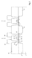
- Fig. 1 is a cross sectional view of two conventional MOS transistors. This drawing is extremely simplified in that only the features useful to the discussion of the present invention are shown.
- Each MOS transistor is formed in a substrate 1, and surrounded by an insulating field region 2 of a certain width, that delimits an active area 3.
- Each MOS transistor comprises a gate dielectric 4, a gate electrode 5, surrounded by insulating spacers 6, source and drain regions 7 and 8 comprising LDD extensions 9 and 10.
- a layer of metal silicide 12 covers the upper surface of the source/drain regions 7, 8.
- a dielectric layer 14 covers the MOS transistor and insulating field regions. Vias 16, 17 contact the source and drain regions 7 and 8.
- Other interconnection structures are formed over the wafer.
- Those skilled in the art will know variations of such a MOS transistor. In particular the MOS transistors are often formed not directly in the substrate but in specifically doped wells of different conductivity types.
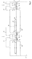
- an anti-fuse cell according to the invention manufactured in an integrated circuit including standard MOS transistors, uses elements identical to at least some of said standard MOS transistors.
- Figure 2 is a cross sectional view illustrating, in the right-hand portion, a standard MOS transistor, and on the left-hand portion, an anti-fuse cell according to an embodiment of the invention.
- the structure on the right-hand portion of figure 2 shall not be disclosed again as it is strictly identical to the structure disclosed in connection with figure 1 .
- the anti-fuse cell according to the invention includes exactly the same elements as the standard MOS transistor shown on the right-hand portion of the figure and, accordingly, the constitutive portions of the anti-fuse cell are designated by the same references.
- the active area around the MOS transistor of an anti-fuse cell is delimited by an insulating field region 22 that is generally wider than the usual insulating field region 2 between standard MOS transistors.
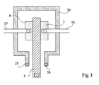
- the internal periphery of the insulating field region in the close neighborhood of the active area is covered by a conductive track 24 that can be better seen in the top view of figure 3 .
- the track 24 includes terminals 25, 26 to which a supply voltage can be applied.
- track 24 is formed simultaneously with the gates of the MOS transistors. This is why, in figure 2 , an underlying insulating layer 27 corresponding to the gate oxide layer 4 and spacers 28 corresponding to the spacers 6 are shown.
- the transistor of the anti-fuse cell according to the invention has the same features as a conventional MOS transistor, i.e. in the absence of a voltage on its gate, it presents a very high resistance between its source and drain terminals 16, 17.
- a voltage is applied to terminals 25, 26 of the conductive track 24. This causes a heating of the neighboring region and in particular of the MOS structure situated inside the track. The heating is selected to be sufficient for obtaining a temperature such that the metal contained in the metal silicide (layers 12 and 13) diffuses inside the silicon.
- the metal of at least one of the source or drain metal silicide attains the substrate through the drain or source region 7 or 8, or the LDD region 9 or 10
- the corresponding junction is no longer rectifying. If only one junction is shorted, the device then operates as a diode. If both drain and source junctions are shorted, the device operates as a resistor. Due to the small size of presently manufactured MOS transistors, this resistor will have a very low value. This value is all the smaller as the diffusion depth from the metal silicide layer is increased.
- the invention draws advantage from the fact that silicon oxide is more thermally insulating than silicon. Accordingly, in particular if the field regions correspond to shallow trench isolation (STI) having a larger depth than the drain and source regions, it will be understood that the region situated at the level of and just under the MOS transistor will undergo a larger temperature increase than the region situated under the conductive track. Also, it will be emphasized that the conductive track is arranged on an internal side of the peripheral field oxide so that the transistors arranged on the other side of the conductive track are not accidentally programmed by the heating.
- STI shallow trench isolation
- the invention provides, in a very simple way, without modifying the usual manufacturing process of a MOS integrated circuit, an efficient anti-fuse cell.
- the anti-fuse according to the invention can be programmed by applying a relatively low voltage to the above-mentioned resistive conductive track 24.
- a relatively low voltage for example, in a technology wherein the gate length is about 60 nm, and by providing a conductive track of a width of 1400 nm at 60 nm from the internal side of an insulating field region having a width of about 4500 nm and a depth of about 300 nm, it will be sufficient to apply a voltage of 3,3 volts at the terminals 25, 26 of the track. This causes a current of about 120 mA to flow in the conductive track during a time that causes a power dissipation of 400 mW.
- the cell according to the invention is programmable with a relatively low voltage compatible with CMOS technologies.
- the active area of the MOS transistor will have a total length of 300 nm and the whole surface of the anti-fuse cell, including the peripheral insulating field region, for example a STI, will be about 5 ⁇ m 2 . So, an anti-fuse cell according to the invention is smaller than most known fuses.
- the result of a desired programming can be simulated before effectively implementing the permanent programming of an array of anti-fuse cells.
- each anti-fuse cell transistor can also operate as a normal transistor.
- the corresponding set of transistors can be made conductive by applying a voltage on their gates. Accordingly, the result of a projected programming can be checked before implementing the programming.
- an anti-fuse cell according to the invention can be programmed in the field, after having put a chip in a package.
- the resistive track according to the invention is generally covered by a relatively thick insulating layer, commonly a CVD oxide, the heating will not result into a substantial temperature increase in the direction of the upper side of the component.
- the silicon is more thermally conductive than an insulator and, in particular a silicon oxide.
- the heat is drawn towards the lower side of the component, due to the fact that, usually, the lower side of a component is linked to a heat sink.
- the conductive track can be made of a plurality of sections or a plurality of concentric conductive tracks could be used.
Landscapes
- Design And Manufacture Of Integrated Circuits (AREA)
- Metal-Oxide And Bipolar Metal-Oxide Semiconductor Integrated Circuits (AREA)
- Semiconductor Memories (AREA)
Claims (10)
- Cellule anti-fusible comprenant :un transistor MOS d'un circuit intégré MOS, avec des régions de source (7) et de drain (8) recouvertes d'une couche de siliciure métallique (12, 13), etau moins une piste (24) d'une couche résistive entourant au moins partiellement ledit transistor MOS, et agencée de manière à laisser passer un courant de chauffage, de telle sorte que le métal de ladite couche de siliciure métallique diffuse au-delà des jonctions de drain et/ou de source.
- Cellule selon la revendication 1, dans laquelle ladite piste résistive est disposée au-dessus d'une région d'isolation du champ (22) entourant ledit transistor MOS, à proximité dudit transistor MOS.
- Cellule selon la revendication 2, dans laquelle la région d'isolation du champ (22) entourant ledit transistor MOS est plus large que les régions d'isolation du champ entourant les autres transistors MOS du même circuit intégré.
- Cellule selon la revendication 1, dans laquelle ladite piste (24) est réalisée dans la même couche que celle utilisée pour former la grille (5) dudit transistor MOS.
- Cellule selon la revendication 1, dans laquelle ladite piste (24) est munie de bornes (25, 26) permettant le passage d'un courant dans celle-ci.
- Procédé de fabrication d'une cellule anti-fusible de la revendication 1 dans un circuit intégré contenant des transistors MOS standard, ayant des régions de source et de drain recouvertes d'une couche de siliciure métallique et étant entourés de régions d'isolement du champ, caractérisé par le fait que chaque cellule anti-fusible est réalisée à partir d'un transistor MOS supplémentaire du même type, et que ledit procédé comprend les étapes suivantes :disposition de régions d'isolement du champ (22) plus larges pour ledit transistor supplémentaire que pour lesdits transistors MOS standard,formation simultanée dudit transistor MOS supplémentaire et desdits transistors MOS standard,formation d'au moins une piste résistive (24) sur la région d'isolement du champ (22) autour de la périphérie dudit transistor MOS supplémentaire, simultanément à la formation de la couche conductrice des grilles des transistors MOS standard.
- Procédé selon la revendication 6, dans lequel le siliciure métallique est un siliciure de nickel.
- Procédé selon la revendication 6, dans lequel chaque transistor MOS a une longueur de grille inférieure à 100 nm.
- Procédé selon la revendication 6, dans lequel chaque région d'isolement du champ a une largeur d'environ 200 nm autour de chaque transistor standard, et une largeur d'environ 5000 nm autour de chaque cellule anti-fusible, lesdites régions d'isolement du champ ayant une profondeur de quelques centaines de nm.
- Procédé selon la revendication 6, comprenant en outre une étape de programmation de fanti-fusible par application, sur la piste résistive (24), d'une tension du même ordre que celui des tensions couramment appliquées pour le fonctionnement du circuit intégré.
Priority Applications (1)
| Application Number | Priority Date | Filing Date | Title |
|---|---|---|---|
| EP05825195A EP1831927B1 (fr) | 2004-12-27 | 2005-12-23 | Cellule anti-fusible et son processus de fabrication |
Applications Claiming Priority (3)
| Application Number | Priority Date | Filing Date | Title |
|---|---|---|---|
| EP04107005 | 2004-12-27 | ||
| EP05825195A EP1831927B1 (fr) | 2004-12-27 | 2005-12-23 | Cellule anti-fusible et son processus de fabrication |
| PCT/EP2005/057150 WO2006069982A1 (fr) | 2004-12-27 | 2005-12-23 | Cellule anti-fusion et son processus de fabrication |
Publications (2)
| Publication Number | Publication Date |
|---|---|
| EP1831927A1 EP1831927A1 (fr) | 2007-09-12 |
| EP1831927B1 true EP1831927B1 (fr) | 2010-04-28 |
Family
ID=35976599
Family Applications (1)
| Application Number | Title | Priority Date | Filing Date |
|---|---|---|---|
| EP05825195A Expired - Lifetime EP1831927B1 (fr) | 2004-12-27 | 2005-12-23 | Cellule anti-fusible et son processus de fabrication |
Country Status (7)
| Country | Link |
|---|---|
| US (1) | US7989914B2 (fr) |
| EP (1) | EP1831927B1 (fr) |
| JP (1) | JP2008526007A (fr) |
| CN (1) | CN100472773C (fr) |
| DE (1) | DE602005020979D1 (fr) |
| TW (1) | TW200629543A (fr) |
| WO (1) | WO2006069982A1 (fr) |
Families Citing this family (11)
| Publication number | Priority date | Publication date | Assignee | Title |
|---|---|---|---|---|
| US20100187638A1 (en) * | 2004-12-27 | 2010-07-29 | Koninklijke Philips Electronics N.V. | Anti-fuse cell and its manufacturing process |
| US7820492B2 (en) * | 2007-05-25 | 2010-10-26 | Kabushiki Kaisha Toshiba | Electrical fuse with metal silicide pipe under gate electrode |
| JP4510057B2 (ja) * | 2007-06-21 | 2010-07-21 | 株式会社東芝 | 不揮発性半導体記憶装置 |
| US8692310B2 (en) | 2009-02-09 | 2014-04-08 | Spansion Llc | Gate fringing effect based channel formation for semiconductor device |
| US8049299B2 (en) | 2009-02-25 | 2011-11-01 | Freescale Semiconductor, Inc. | Antifuses with curved breakdown regions |
| US8542517B2 (en) | 2011-06-13 | 2013-09-24 | International Business Machines Corporation | Low voltage programmable mosfet antifuse with body contact for diffusion heating |
| CN102254846B (zh) * | 2011-07-04 | 2016-01-27 | 上海华虹宏力半导体制造有限公司 | 半导体器件中金属硅化物层电阻的仿真方法 |
| US8815736B2 (en) * | 2011-08-25 | 2014-08-26 | Globalfoundries Inc. | Methods of forming metal silicide regions on semiconductor devices using different temperatures |
| CN103456710B (zh) * | 2012-06-04 | 2016-06-01 | 中芯国际集成电路制造(上海)有限公司 | Mos器件及其制造方法 |
| CN105849861B (zh) * | 2014-04-03 | 2018-08-10 | 新诺普系统公司 | 反熔丝存储器单元 |
| US9455222B1 (en) * | 2015-12-18 | 2016-09-27 | Texas Instruments Incorporated | IC having failsafe fuse on field dielectric |
Citations (1)
| Publication number | Priority date | Publication date | Assignee | Title |
|---|---|---|---|---|
| US5019878A (en) * | 1989-03-31 | 1991-05-28 | Texas Instruments Incorporated | Programmable interconnect or cell using silicided MOS transistors |
Family Cites Families (9)
| Publication number | Priority date | Publication date | Assignee | Title |
|---|---|---|---|---|
| JP3086247B2 (ja) * | 1990-11-27 | 2000-09-11 | 株式会社東芝 | 半導体メモリセル |
| JPH04294577A (ja) * | 1991-03-22 | 1992-10-19 | Ricoh Co Ltd | プログラム可能な半導体装置 |
| US5298784A (en) * | 1992-03-27 | 1994-03-29 | International Business Machines Corporation | Electrically programmable antifuse using metal penetration of a junction |
| US20030109125A1 (en) * | 2001-12-10 | 2003-06-12 | Chewnpu Jou | Fuse structure for a semiconductor device and manufacturing method thereof |
| US6794726B2 (en) * | 2002-04-17 | 2004-09-21 | International Business Machines Corporation | MOS antifuse with low post-program resistance |
| US20040124458A1 (en) * | 2002-12-31 | 2004-07-01 | Chandrasekharan Kothandaraman | Programmable fuse device |
| JP2004241558A (ja) * | 2003-02-05 | 2004-08-26 | Toshiba Corp | 不揮発性半導体記憶装置及びその製造方法、半導体集積回路及び不揮発性半導体記憶装置システム |
| US7180102B2 (en) * | 2003-09-30 | 2007-02-20 | Agere Systems Inc. | Method and apparatus for using cobalt silicided polycrystalline silicon for a one time programmable non-volatile semiconductor memory |
| US7439168B2 (en) * | 2004-10-12 | 2008-10-21 | Dcg Systems, Inc | Apparatus and method of forming silicide in a localized manner |
-
2005
- 2005-12-19 TW TW094144994A patent/TW200629543A/zh unknown
- 2005-12-23 US US11/793,990 patent/US7989914B2/en active Active
- 2005-12-23 DE DE602005020979T patent/DE602005020979D1/de not_active Expired - Lifetime
- 2005-12-23 EP EP05825195A patent/EP1831927B1/fr not_active Expired - Lifetime
- 2005-12-23 WO PCT/EP2005/057150 patent/WO2006069982A1/fr not_active Ceased
- 2005-12-23 CN CNB2005800449382A patent/CN100472773C/zh not_active Expired - Fee Related
- 2005-12-23 JP JP2007547544A patent/JP2008526007A/ja active Pending
Patent Citations (1)
| Publication number | Priority date | Publication date | Assignee | Title |
|---|---|---|---|---|
| US5019878A (en) * | 1989-03-31 | 1991-05-28 | Texas Instruments Incorporated | Programmable interconnect or cell using silicided MOS transistors |
Also Published As
| Publication number | Publication date |
|---|---|
| DE602005020979D1 (de) | 2010-06-10 |
| US7989914B2 (en) | 2011-08-02 |
| US20090102014A1 (en) | 2009-04-23 |
| WO2006069982A1 (fr) | 2006-07-06 |
| EP1831927A1 (fr) | 2007-09-12 |
| TW200629543A (en) | 2006-08-16 |
| CN100472773C (zh) | 2009-03-25 |
| JP2008526007A (ja) | 2008-07-17 |
| CN101091249A (zh) | 2007-12-19 |
Similar Documents
| Publication | Publication Date | Title |
|---|---|---|
| US9184129B2 (en) | Three-terminal antifuse structure having integrated heating elements for a programmable circuit | |
| US7227238B2 (en) | Integrated fuse with regions of different doping within the fuse neck | |
| JP5253522B2 (ja) | Mosfetフューズ素子を有する集積回路 | |
| US7960809B2 (en) | eFuse with partial SiGe layer and design structure therefor | |
| KR101873281B1 (ko) | 안티퓨즈 메모리 셀 | |
| US20060046354A1 (en) | Recessed gate dielectric antifuse | |
| US20070029576A1 (en) | Programmable semiconductor device containing a vertically notched fusible link region and methods of making and using same | |
| US20060220174A1 (en) | E-Fuse and anti-E-Fuse device structures and methods | |
| KR20070025917A (ko) | 퓨즈 소자 및 그 절단 방법 | |
| EP1831927B1 (fr) | Cellule anti-fusible et son processus de fabrication | |
| US5789794A (en) | Fuse structure for an integrated circuit element | |
| TWI469339B (zh) | 反熔絲元件及用於控制破裂位置之電氣冗餘反熔絲陣列 | |
| KR101385251B1 (ko) | 멀티 레벨 안티 퓨즈 및 그 동작 방법 | |
| US5572050A (en) | Fuse-triggered antifuse | |
| TWI399847B (zh) | 可調諧反熔絲元件及其製造方法 | |
| US20060157819A1 (en) | Efuse structure | |
| KR20090103613A (ko) | 안티퓨즈 및 그 동작방법 | |
| US7436044B2 (en) | Electrical fuses comprising thin film transistors (TFTS), and methods for programming same | |
| US8674475B2 (en) | Antifuse and methods of operating and manufacturing the same | |
| US20090029541A1 (en) | Method of fabricating anti-fuse and method of programming anti-fuse | |
| US20100187638A1 (en) | Anti-fuse cell and its manufacturing process | |
| KR101936921B1 (ko) | 반도체 소자의 안티퓨즈 및 그의 형성 방법 | |
| US20260040538A1 (en) | One-time programmable memory cell | |
| KR20110109548A (ko) | 반도체 소자의 안티퓨즈 및 그의 형성 방법 | |
| HK1003959A (en) | Fuse structure for an integrated circuit device |
Legal Events
| Date | Code | Title | Description |
|---|---|---|---|
| PUAI | Public reference made under article 153(3) epc to a published international application that has entered the european phase |
Free format text: ORIGINAL CODE: 0009012 |
|
| 17P | Request for examination filed |
Effective date: 20070618 |
|
| AK | Designated contracting states |
Kind code of ref document: A1 Designated state(s): DE FR GB IT |
|
| DAX | Request for extension of the european patent (deleted) | ||
| RBV | Designated contracting states (corrected) |
Designated state(s): DE FR GB IT |
|
| RAP1 | Party data changed (applicant data changed or rights of an application transferred) |
Owner name: NXP B.V. Owner name: STMICROELETRONICS CROLLES 2 SAS |
|
| GRAP | Despatch of communication of intention to grant a patent |
Free format text: ORIGINAL CODE: EPIDOSNIGR1 |
|
| GRAS | Grant fee paid |
Free format text: ORIGINAL CODE: EPIDOSNIGR3 |
|
| GRAA | (expected) grant |
Free format text: ORIGINAL CODE: 0009210 |
|
| AK | Designated contracting states |
Kind code of ref document: B1 Designated state(s): DE FR GB IT |
|
| REG | Reference to a national code |
Ref country code: GB Ref legal event code: FG4D |
|
| REF | Corresponds to: |
Ref document number: 602005020979 Country of ref document: DE Date of ref document: 20100610 Kind code of ref document: P |
|
| PGFP | Annual fee paid to national office [announced via postgrant information from national office to epo] |
Ref country code: FR Payment date: 20101224 Year of fee payment: 6 |
|
| PLBE | No opposition filed within time limit |
Free format text: ORIGINAL CODE: 0009261 |
|
| STAA | Information on the status of an ep patent application or granted ep patent |
Free format text: STATUS: NO OPPOSITION FILED WITHIN TIME LIMIT |
|
| PG25 | Lapsed in a contracting state [announced via postgrant information from national office to epo] |
Ref country code: IT Free format text: LAPSE BECAUSE OF FAILURE TO SUBMIT A TRANSLATION OF THE DESCRIPTION OR TO PAY THE FEE WITHIN THE PRESCRIBED TIME-LIMIT Effective date: 20100428 |
|
| PGFP | Annual fee paid to national office [announced via postgrant information from national office to epo] |
Ref country code: GB Payment date: 20101222 Year of fee payment: 6 |
|
| 26N | No opposition filed |
Effective date: 20110131 |
|
| PGFP | Annual fee paid to national office [announced via postgrant information from national office to epo] |
Ref country code: DE Payment date: 20101215 Year of fee payment: 6 |
|
| GBPC | Gb: european patent ceased through non-payment of renewal fee |
Effective date: 20111223 |
|
| REG | Reference to a national code |
Ref country code: FR Ref legal event code: ST Effective date: 20120831 |
|
| REG | Reference to a national code |
Ref country code: DE Ref legal event code: R119 Ref document number: 602005020979 Country of ref document: DE Effective date: 20120703 |
|
| PG25 | Lapsed in a contracting state [announced via postgrant information from national office to epo] |
Ref country code: GB Free format text: LAPSE BECAUSE OF NON-PAYMENT OF DUE FEES Effective date: 20111223 Ref country code: DE Free format text: LAPSE BECAUSE OF NON-PAYMENT OF DUE FEES Effective date: 20120703 |
|
| PG25 | Lapsed in a contracting state [announced via postgrant information from national office to epo] |
Ref country code: FR Free format text: LAPSE BECAUSE OF NON-PAYMENT OF DUE FEES Effective date: 20120102 |