EP1831957B1 - Schlitzantenne mit einem mems-varaktor zur resonanzfrequenzabstimmung - Google Patents
Schlitzantenne mit einem mems-varaktor zur resonanzfrequenzabstimmung Download PDFInfo
- Publication number
- EP1831957B1 EP1831957B1 EP05853644A EP05853644A EP1831957B1 EP 1831957 B1 EP1831957 B1 EP 1831957B1 EP 05853644 A EP05853644 A EP 05853644A EP 05853644 A EP05853644 A EP 05853644A EP 1831957 B1 EP1831957 B1 EP 1831957B1
- Authority
- EP
- European Patent Office
- Prior art keywords
- antenna
- varactors
- slot
- secondary slots
- slot antenna
- Prior art date
- Legal status (The legal status is an assumption and is not a legal conclusion. Google has not performed a legal analysis and makes no representation as to the accuracy of the status listed.)
- Expired - Lifetime
Links
Images


Classifications
-
- H—ELECTRICITY
- H01—ELECTRIC ELEMENTS
- H01Q—ANTENNAS, i.e. RADIO AERIALS
- H01Q13/00—Waveguide horns or mouths; Slot antennas; Leaky-waveguide antennas; Equivalent structures causing radiation along the transmission path of a guided wave
- H01Q13/10—Resonant slot antennas
- H01Q13/103—Resonant slot antennas with variable reactance for tuning the antenna
Definitions
- Miniaturized antennas are effective for utilization in mobile wireless communication applications, particularly for handheld devices such as cell phones and personal digital assistants that may incorporate a radio-frequency communication system.
- Miniaturized slot antennas have been described and designed. When the size of an antenna is reduced, its bandwidth is also reduced accordingly. As a result, miniaturized antennas having a size suitable for handheld devices may have a bandwidth that is too narrow to cover the pass band of a communication standard that is desired for the handheld devices to utilize.
- GB 2 304 464 A discloses a slot antenna device comprising an electrically conductive plate 211 and a slot therein, both being L-shaped and mounted on a dielectric substrate.
- US-B1-6 355 534 discloses an improved variable tunable range MEMS and a method of making comprising stiffening a movable charge plate; making variable capacitance a more linear function of the actuation force applied; and a larger tuning range.
- US-B2-6 593 672 discloses a MEMS-switched stepped variable capacitor and method of making comprising a wide range of capacitances built into a single capacitor which is also variable between stepped capacitances.
- Carrasquillo-Rivera H et al, "Tunable and dual-band rectangular slot-ring antenna” Antennas and Propogation Society Symposium 2004 IEEE Monterey, CA, USA vol.4, 20 June 2004 pages 4308-4311 discloses a tunable and dual-band rectangular slot-ring antenna comprising lateral slots cut in a substrate, together forming an unclosed rectangle. Two further slots connect the two ends of the unclosed rectangle to the edge of the substrate.
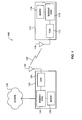
- FIG. 1 is a block diagram of a wireless local area or cellular network communication system in accordance with one or more embodiments of the present invention
- FIG. 2 is a schematic diagram of a slot antenna having a MEMS varactor for resonance frequency tuning in accordance with one or more embodiments of the present invention
- FIG. 3 is a schematic diagram of an alternative slot antenna having a MEMS varactor in accordance with one or more embodiments of the present invention
- FIGS. 4A, 4B, and 4C are schematic diagrams of a MEMS varactor suitable for utilization in a slot antenna in accordance with one or more embodiments of the present invention.
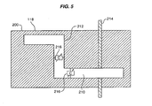
- FIG. 5 is a schematic diagram of a general case slot antenna having a MEMS varactor.
- Coupled may mean that two or more elements are in direct physical or electrical contact.
- coupled may also mean that two or more elements may not be in direct contact with each other, but yet may still cooperate or interact with each other.
- Radio systems intended to be included within the scope of the present invention include, by way of example only, wireless local area networks (WLAN) devices and wireless wide area network (WWAN) devices including wireless network interface devices and network interface cards (NICs), base stations, access points (APs), gateways, bridges, hubs, cellular radiotelephone communication systems, satellite communication systems, two-way radio communication systems, one-way pagers, two-way pagers, personal communication systems (PCS), personal computers (PCs), personal digital assistants (PDAs), and the like, although the scope of the invention is not limited in this respect.
- WLAN wireless local area networks
- WWAN wireless wide area network
- NICs network interface cards
- APs access points
- gateways gateways
- bridges bridges
- hubs hubs
- cellular radiotelephone communication systems satellite communication systems
- two-way radio communication systems one-way pagers, two-way pagers
- PCS personal communication systems
- PCs personal computers
- PDAs personal digital assistants
- Types of wireless communication systems intended to be within the scope of the present invention include, although not limited to, Wireless Local Area Network (WLAN), Wireless Wide Area Network (WWAN), Code Division Multiple Access (CDMA) cellular radiotelephone communication systems, Global System for Mobile Communications (GSM) cellular radiotelephone systems, North American Digital Cellular (NADC) cellular radiotelephone systems, Time Division Multiple Access (TDMA) systems, Extended-TDMA (E-TDMA) cellular radiotelephone systems, Third Generation Partnership Project (3GPP or 3G) systems like Wide-band CDMA (WCDMA), CDMA-2000, and the like, although the scope of the invention is not limited in this respect.
- WLAN Wireless Local Area Network
- WWAN Wireless Wide Area Network
- CDMA Code Division Multiple Access
- GSM Global System for Mobile Communications
- NADC North American Digital Cellular
- TDMA Time Division Multiple Access
- E-TDMA Extended-TDMA
- 3GPP or 3G Third Generation Partnership Project
- WCDMA Wide-band CDMA
- CDMA-2000 Code Division Multiple Access-2000
- a mobile unit 110 may include a wireless transceiver 112 to couple to an antenna 118 and to a processor 114 to provide baseband and media access control (MAC) processing functions.
- antenna 118 may be a slot antenna having a MEMS varactor for resonant frequency tuning of the antenna as show in and described with respect to FIGS. 2, 3 , and 4 , although the scope of the invention is not limited in this respect.
- mobile unit 110 may be a cellular telephone or an information handling system such as a mobile personal computer or a personal digital assistant or the like that incorporates a cellular telephone communication module, although the scope of the invention is not limited in this respect.
- Processor 114 in one embodiment may comprise a single processor, or alternatively may comprise a baseband processor and an applications processor, although the scope of the invention is not limited in this respect.
- Processor 114 may couple to a memory 116 which may include volatile memory such as dynamic random-access memory (DRAM), non-volatile memory such as flash memory, or alternatively may include other types of storage such as a hard disk drive, although the scope of the invention is not limited in this respect.
- DRAM dynamic random-access memory
- flash memory non-volatile memory
- other types of storage such as a hard disk drive
- memory 116 may be included on the same integrated circuit as processor 114, or alternatively some portion or all of memory 116 may be disposed on an integrated circuit or other medium, for example a hard disk drive, that is external to the integrated circuit of processor 114, although the scope of the invention is not limited in this respect.
- Mobile unit 110 may communicate with access point 122 via wireless communication link 132, where access point 122 may include at least one antenna 120, transceiver 124, processor 126, and memory 128.
- access point 122 may be a base station of a cellular telephone network, and in an alternative embodiment, access point 122 may be a an access point or wireless router of a wireless local or personal area network, although the scope of the invention is not limited in this respect.
- access point 122 and optionally mobile unit 110 may include two or more antennas, for example to provide a spatial division multiple access (SDMA) system or a multiple input, multiple output (MIMO) system, although the scope of the invention is not limited in this respect.
- SDMA spatial division multiple access
- MIMO multiple input, multiple output
- Access point 122 may couple with network 130 so that mobile unit 110 may communicate with network 130, including devices coupled to network 130, by communicating with access point 122 via wireless communication link 132.
- Network 130 may include a public network such as a telephone network or the Internet, or alternatively network 130 may include a private network such as an intranet, or a combination of a public and a private network, although the scope of the invention is not limited in this respect.
- Communication between mobile unit 110 and access point 122 may be implemented via a wireless local area network (WLAN), for example a network compliant with a an Institute of Electrical and Electronics Engineers (IEEE) standard such as IEEE 802.11 a, IEEE 802.11 b, HiperLAN-II, and so on, although the scope of the invention is not limited in this respect.
- IEEE Institute of Electrical and Electronics Engineers
- communication between mobile unit 110 and access point 122 may be at least partially implemented via a cellular communication network compliant with a Third Generation Partnership Project (3GPP or 3G) standard, although the scope of the invention is not limited in this respect.
- antenna 118 may be utilized in a wireless sensor network or a mesh network, although the scope of the invention is not limited in this respect.
- Antenna 118 is a slot antenna that may be constructed from a planar layer 200 which may be a conductive material such as a metal.
- Planar layer 200 may generally lie within a plane, but may also alternatively be arranged into other non-planar forms and shapes, and the scope of the invention is not limited in this respect.
- Planar layer 200 may be referred to generally as an antenna layer, although the scope of the invention is not limited in this respect.
- Planar layer 200 has a primary slot 210 and one or more secondary slots 212 formed thereon.
- Primary slot 210 and secondary slots 212 function as radiators having dimensions selected to provide a half wavelength antenna to operate as a dipole antenna.
- the inductance of antenna 118 is increased.
- the size of antenna 118 may be decreased by the addition of a greater number of secondary slots 212.
- antenna 118 may be further decreased by increasing the inductance of secondary slots 212, for example by increasing the length of secondary slots 212 or by the selected shape of secondary slots 212, for example by providing a folded or coiled shape to secondary slots 212.
- An example of an antenna having an alternatively shaped secondary slot is shown in and described with respect to FIG. 3 .
- a microstrip feed 214 may couple antenna 118 to a radio-frequency circuit such as transceiver 112, although the scope of the invention is not limited in this respect.
- the antenna 118 may be selectively tuned by utilization of one or more varactors 216 to couple to one or more secondary slots 212.
- one of secondary slots 212 includes a varactor 212
- two or more of secondary slots 212 may include one or more varactors 216
- all or most of secondary slots 212 may include one or more varactors 216, although the scope of the invention is not limited in this respect.
- one or more varactors 216 may be optionally included in primary slot 210 in combination with one or more varactors 216 in secondary slots 212, although the scope of the invention is not limited in this respect.
- a varactor 216 may generally be referred to as a variable capacitor having a varying or selectable capacitance.
- varactor 216 may be a microelectromechanical system (MEMS) based varactor such as shown in and described with respect to FIG. 4 , and in another embodiment of the invention varactor 216 may include a varactor diode, although the scope of the invention is not limited in this respect.
- a capacitance value is applied to one or more of secondary slots 212 to reduced the inductance of one or more secondary slots 212 and to reduce the inductance of antenna 118 at one or more desired frequencies.
- the capacitance of one or more varactors 216 in combination with the inductance of one or more secondary slots 212 or the inductance of antenna 118 provides a resonant circuit that may be utilized to selectively tune the resonant frequency of antenna 118 via selective actuating one or more of varactors 216 or via selectively setting the capacitance value of one or more varactors 216 to a capacitance that may cause a resonant frequency of antenna 118 to be tuned to a desired frequency of operation of antenna 118. For example, when the selected capacitance is increased in value, the inductance of antenna 118 may be reduced, and the resonant frequency of antenna 118 may be increased to a desired frequency of operation, although the scope of the invention is not limited in this respect.
- a pass band for a cellular communication system such a communication system 100 as shown in and described with respect to FIG. 1 may be divided into one or more channels, for example where the channels may have a bandwidth one the order of a few kilohertz.
- the resonance of antenna 118 is tuned via varactors 216 to a desired channel wherein antenna 118 may have a resonant frequency that is tuned to the desired channel.
- varactor 216 is a MEMS varactor
- the Q factor of varactor 216 may be relatively high, and the loss of antenna 118 may be relatively low, resulting in a narrow band mode of operation for antenna 118 to provide a relatively higher noise rejection characteristic, although the scope of the invention is not limited in this respect.
- the resonant frequency of antenna 118 may be selected via changing the capacitance of varactor 216 to tune antenna 118 to the other channel, although the scope of the invention is not limited in this respect.
- secondary slots 216 may be constructed to have a longer length than secondary slots 212 as shown in FIG. 2 . In such a configuration, there may be a greater inductance per secondary slot 212 which may allow for a greater reduction in the size of antenna 118.
- secondary slots 212 may be further arranged in a coil shape to provide an increased inductance per secondary slot 212, which may be for example a result of an increased self inductance for the secondary slots 212 provided by the coiled or folded structure of secondary slot 212. As discussed with respect to FIG.
- one or more varactors 216 may be coupled to one or more secondary slots 212 to selectively tune the resonant frequency of antenna 118 to a desired frequency or channel. Furthermore, in one or more alternative embodiments, one or more varactors 216 may be optionally included in primary slot 210 in combination with one or more varactors 216 in secondary slots 212, although the scope of the invention is not limited in this respect.
- varactor 216 may be constructed as a MEMS structure to provide a controllable or selectable capacitance via actuation of varactor 216.
- a top plan view of varactor 216 is shown at 400, an isometric view of varactor 216 in a stand-by state 410 is shown at 402, and an isometric view of varactor 216 in an actuated state 412 is shown at 404.
- Varactor 216 may be a MEMS structure such as a plate 418 suspended above a plane 414 in a stand-by state 410. While in stand-by state 410, the capacitance value of varactor 216 may be a smaller value capacitance or effectively a zero value capacitance. When selected or actuated in actuation state 412, plate 418 may be deflected closer to plane 414 to provide a resulting capacitance value between plate 418 and plane 414. The closer that plate 418 is deflected toward plane 414, the greater the resulting capacitance value is provided by varactor 216, although the scope of the invention is not limited in this respect.
- one or more of varactors 216 may be a variable tuning range capacitor as shown and described in US Patent No. 6,355,534 .
- a phase locked loop circuit (not shown) may be coupled to one or more of varactors 216 to set the capacitance value of one or more of varactors 216 to lock the resonant frequency of antenna 118 on a desired frequency of operation, although the scope of the invention is not limited in this respect.
- a planar layer 200 of a general case antenna 118 may include a slot primary 210 of any arbitrary shape, and may also have one or more secondary slots 212 also having any arbitrary shape.
- a pass band for cellular communication may be divided into several channels, for example where each channel may have a bandwidth on the order of a few kilohertz.
- the resonant frequency of antenna 118 may be tuned to a desired channel in the pass band to cause an otherwise wider band antenna to operate as a narrow band antenna when tuned to the desired channel.
- One or more varactors 216 may be disposed in a slot 210 or 212 of antenna 118 and may provide frequency tuning of the resonant frequency of antenna 118 to the desired channel.
- one or more of slots 210 and 212 may have an arbitrary shape.
- One or more of varactors 216 may be utilized to selectively reduce an effective inductance of the antenna.
- the resonant frequency of antenna 118 may be tuned by changing the capacitance of the varactors, although the scope of the invention is not limited in this respect.
Landscapes
- Support Of Aerials (AREA)
- Waveguide Aerials (AREA)
- Variable-Direction Aerials And Aerial Arrays (AREA)
- Input Circuits Of Receivers And Coupling Of Receivers And Audio Equipment (AREA)
Claims (11)
- Vorrichtung, umfassend
eine Antennenschicht (200) mit einem primären Schlitz (210) , der vollständig in der Antennenschicht (200) gebildet ist, wobei der primäre Schlitz (210) einen Rand der Antennenschicht (200) nicht berührt;
einen oder mehrere sekundäre Schlitze (212), die vollständig in der Antennenschicht (200) gebildet sind, um eine Schlitzantenne zu bilden,
dadurch gekennzeichnet, dass der eine oder die mehreren sekundären Schlitze (212) den primären Schlitz (210) jeweils rechtwinkelig kreuzen und sich an beiden Seiten davon erstrecken, wobei die sekundären Schlitze (212) den Rand der Antennenschicht nicht berühren; und
einer oder mehrere Varaktoren (216) mit einem oder mehreren der sekundären Schlitze (212) gekoppelt sind und nicht über die rechtwinkelige Schnittlinie verbunden sind, um die Schlitzantenne über die Wahl einer Kapazität eines oder mehrerer der varaktoren (216) auf eine gewünschte Frequenz abzustimmen. - Vorrichtung nach Anspruch 1, wobei die Varaktoren (216) Aufbauten aus einem mikroelektromechanischen System sind.
- Vorrichtung nach Anspruch 1, wobei die Schlitzantenne über die Varaktoren (216) auf einen Kanal eines zellularen Kommunikationssystems abgestimmt werden kann.
- Vorrichtung nach Anspruch 1, wobei die Schlitzantenne über die Varaktoren (216) auf einen Kanal eines drahtlosen lokalen Kommunikationssystems abgestimmt werden kann.
- Vorrichtung nach Anspruch 1, wobei der eine oder die mehreren sekundären schlitze (212) gefaltet sind, um dem sekundären Schlitz (212) eine erhöhte Induktivität bereitzustellen.
- Vorrichtung nach Anspruch 1, wobei die Schlitzantenne auf Basis eines höheren Gütefaktors der Varaktoren (216) einen höheren Gütefaktor aufweist.
- Vorrichtung nach Anspruch 1, wobei eine Induktivität der sekundären Schlitze (212) in Kombination mit einer Kapazität der Varaktoren (216) der Schlitzantenne eine Schmalbandcharakteristik verleiht.
- Vorrichtung nach Anspruch 1, wobei einer oder mehrere der Varaktoren (216) einen fortlaufend wählbaren Kapazitätswert aufweisen.
- Vorrichtung nach Anspruch 1, wobei einer oder mehrere der Varaktoren (216) eine diskretwertig wählbare Kapazität aufweist.
- Vorrichtung nach Anspruch 1, wobei, einer oder mehrere der Varaktoren (216) ein Netz von wählbaren Kondensatoren umfasst, um einen stufig veränderlichen Kapazitätswert bereitzustellen.
- Vorrichtung, umfassend
einen Basisbandprozessor, um Basisbandzellulartelefoninformationen zu verarbeiten;
einen Sender-Empfänger zur Koppelung mit dem Basisbandprozessor; und
eine Schlitzantenne gemäß der Vorrichtung nach einem der Ansprüche 1 bis 10.
Applications Claiming Priority (2)
| Application Number | Priority Date | Filing Date | Title |
|---|---|---|---|
| US11/013,594 US7348928B2 (en) | 2004-12-14 | 2004-12-14 | Slot antenna having a MEMS varactor for resonance frequency tuning |
| PCT/US2005/044776 WO2006065693A1 (en) | 2004-12-14 | 2005-12-09 | Slot antenna having a mems varactor for resonance frequency tuning |
Publications (2)
| Publication Number | Publication Date |
|---|---|
| EP1831957A1 EP1831957A1 (de) | 2007-09-12 |
| EP1831957B1 true EP1831957B1 (de) | 2009-01-28 |
Family
ID=36090776
Family Applications (1)
| Application Number | Title | Priority Date | Filing Date |
|---|---|---|---|
| EP05853644A Expired - Lifetime EP1831957B1 (de) | 2004-12-14 | 2005-12-09 | Schlitzantenne mit einem mems-varaktor zur resonanzfrequenzabstimmung |
Country Status (6)
| Country | Link |
|---|---|
| US (1) | US7348928B2 (de) |
| EP (1) | EP1831957B1 (de) |
| JP (1) | JP4494475B2 (de) |
| AT (1) | ATE422103T1 (de) |
| DE (1) | DE602005012601D1 (de) |
| WO (1) | WO2006065693A1 (de) |
Families Citing this family (57)
| Publication number | Priority date | Publication date | Assignee | Title |
|---|---|---|---|---|
| US7957277B2 (en) * | 2005-02-25 | 2011-06-07 | Interdigital Technology Corporation | Wireless communication method and system for routing packets via intra-mesh and extra-mesh routes |
| US9130602B2 (en) | 2006-01-18 | 2015-09-08 | Qualcomm Incorporated | Method and apparatus for delivering energy to an electrical or electronic device via a wireless link |
| US8447234B2 (en) * | 2006-01-18 | 2013-05-21 | Qualcomm Incorporated | Method and system for powering an electronic device via a wireless link |
| US7773041B2 (en) | 2006-07-12 | 2010-08-10 | Apple Inc. | Antenna system |
| JP4883573B2 (ja) * | 2006-12-06 | 2012-02-22 | 独立行政法人産業技術総合研究所 | アンテナとそれを用いた発振器 |
| US9774086B2 (en) | 2007-03-02 | 2017-09-26 | Qualcomm Incorporated | Wireless power apparatus and methods |
| US8378522B2 (en) | 2007-03-02 | 2013-02-19 | Qualcomm, Incorporated | Maximizing power yield from wireless power magnetic resonators |
| US9124120B2 (en) * | 2007-06-11 | 2015-09-01 | Qualcomm Incorporated | Wireless power system and proximity effects |
| US7612725B2 (en) * | 2007-06-21 | 2009-11-03 | Apple Inc. | Antennas for handheld electronic devices with conductive bezels |
| JP5697979B2 (ja) | 2007-08-09 | 2015-04-08 | クゥアルコム・インコーポレイテッドQualcomm Incorporated | ワイヤレスに電力供給および充電するためのシステムおよび方法 |
| JP2010539857A (ja) | 2007-09-17 | 2010-12-16 | クゥアルコム・インコーポレイテッド | ワイヤレスエネルギー伝送のための送信機および受信機 |
| EP2208279A4 (de) | 2007-10-11 | 2016-11-30 | Qualcomm Inc | Drahtloser stromtransfer unter verwendung von magnetomechanischen systemen |
| US8629576B2 (en) | 2008-03-28 | 2014-01-14 | Qualcomm Incorporated | Tuning and gain control in electro-magnetic power systems |
| US8106836B2 (en) | 2008-04-11 | 2012-01-31 | Apple Inc. | Hybrid antennas for electronic devices |
| US7773044B2 (en) * | 2008-04-25 | 2010-08-10 | Nokia Corporation | Method for enhancing an antenna performance, antenna, and apparatus |
| US20090273242A1 (en) * | 2008-05-05 | 2009-11-05 | Nigelpower, Llc | Wireless Delivery of power to a Fixed-Geometry power part |
| US8665164B2 (en) * | 2008-11-19 | 2014-03-04 | Apple Inc. | Multiband handheld electronic device slot antenna |
| US8800318B2 (en) * | 2009-01-09 | 2014-08-12 | Donald Charles Erickson | Hybrid spray absorber |
| US8588686B2 (en) | 2009-06-09 | 2013-11-19 | Broadcom Corporation | Method and system for remote power distribution and networking for passive devices |
| US8508422B2 (en) * | 2009-06-09 | 2013-08-13 | Broadcom Corporation | Method and system for converting RF power to DC power utilizing a leaky wave antenna |
| US8320856B2 (en) * | 2009-06-09 | 2012-11-27 | Broadcom Corporation | Method and system for a leaky wave antenna as a load on a power amplifier |
| US8660500B2 (en) | 2009-06-09 | 2014-02-25 | Broadcom Corporation | Method and system for a voltage-controlled oscillator with a leaky wave antenna |
| US9172139B2 (en) * | 2009-12-03 | 2015-10-27 | Apple Inc. | Bezel gap antennas |
| US8270914B2 (en) * | 2009-12-03 | 2012-09-18 | Apple Inc. | Bezel gap antennas |
| US9160056B2 (en) | 2010-04-01 | 2015-10-13 | Apple Inc. | Multiband antennas formed from bezel bands with gaps |
| US9070969B2 (en) | 2010-07-06 | 2015-06-30 | Apple Inc. | Tunable antenna systems |
| US8947303B2 (en) | 2010-12-20 | 2015-02-03 | Apple Inc. | Peripheral electronic device housing members with gaps and dielectric coatings |
| WO2012084057A1 (en) | 2010-12-23 | 2012-06-28 | Epcos Ag | Rf device and method for tuning an rf device |
| US9166300B2 (en) * | 2011-02-09 | 2015-10-20 | Nec Corporation | Slot antenna |
| US9246221B2 (en) | 2011-03-07 | 2016-01-26 | Apple Inc. | Tunable loop antennas |
| US9166279B2 (en) * | 2011-03-07 | 2015-10-20 | Apple Inc. | Tunable antenna system with receiver diversity |
| US9570420B2 (en) | 2011-09-29 | 2017-02-14 | Broadcom Corporation | Wireless communicating among vertically arranged integrated circuits (ICs) in a semiconductor package |
| JP5403637B2 (ja) * | 2011-10-03 | 2014-01-29 | 独立行政法人産業技術総合研究所 | アンテナとそれを用いた発振器 |
| US9350069B2 (en) | 2012-01-04 | 2016-05-24 | Apple Inc. | Antenna with switchable inductor low-band tuning |
| US9190712B2 (en) | 2012-02-03 | 2015-11-17 | Apple Inc. | Tunable antenna system |
| US9379431B2 (en) * | 2012-10-08 | 2016-06-28 | Taoglas Group Holdings Limited | Electromagnetic open loop antenna with self-coupling element |
| US9287630B2 (en) * | 2012-12-03 | 2016-03-15 | Intel Corporation | Dual-band folded meta-inspired antenna with user equipment embedded wideband characteristics |
| US9601267B2 (en) | 2013-07-03 | 2017-03-21 | Qualcomm Incorporated | Wireless power transmitter with a plurality of magnetic oscillators |
| KR102026739B1 (ko) * | 2013-09-02 | 2019-09-30 | 삼성전자주식회사 | 가변성 나노 안테나와 그 제조 및 방법 |
| US10003131B2 (en) | 2013-11-19 | 2018-06-19 | At&T Intellectual Property I, L.P. | System and method of optical antenna tuning |
| WO2015104409A1 (en) * | 2014-01-13 | 2015-07-16 | Thomson Licensing | Slot line resonator for filters |
| US10739437B2 (en) * | 2015-01-26 | 2020-08-11 | Nec Corporation | Frequency selective surface, wireless communication device, and radar device |
| US10176422B2 (en) | 2015-06-09 | 2019-01-08 | Assa Abloy Ab | RIFD tag with a tunable antenna |
| CN107851889B (zh) | 2015-07-24 | 2020-10-30 | Agc株式会社 | 玻璃天线和具有玻璃天线的车辆用窗玻璃 |
| CN107851890B (zh) | 2015-07-24 | 2020-12-22 | Agc株式会社 | 玻璃天线和具有玻璃天线的车辆用窗玻璃 |
| KR101723843B1 (ko) * | 2015-09-13 | 2017-04-07 | 주식회사 아이엠텍 | 휴대 단말기 |
| KR20170032498A (ko) * | 2015-09-13 | 2017-03-23 | 주식회사 아이엠텍 | 휴대 단말기 |
| US9698495B2 (en) | 2015-10-01 | 2017-07-04 | King Fahd University Of Petroleum And Minerals | Reconfigurable MIMO and sensing antenna system |
| US20170301475A1 (en) * | 2016-04-15 | 2017-10-19 | Kymeta Corporation | Rf resonators with tunable capacitor and methods for fabricating the same |
| CN106025562B (zh) * | 2016-06-27 | 2018-06-05 | 北京航空航天大学 | 一种具有耦合抑制窄带的缝隙天线 |
| TWI635653B (zh) * | 2017-04-18 | 2018-09-11 | 華碩電腦股份有限公司 | 天線元件 |
| US10296821B2 (en) | 2017-08-17 | 2019-05-21 | Assa Abloy Ab | RFID devices and methods of making the same |
| US11342671B2 (en) | 2019-06-07 | 2022-05-24 | Sonos, Inc. | Dual-band antenna topology |
| US10790590B1 (en) * | 2019-11-06 | 2020-09-29 | United Arab Emirates University | Frequency agile antenna |
| JP7575305B2 (ja) * | 2021-03-12 | 2024-10-29 | 大王製紙株式会社 | Rfidタグ及びrfidタグの製造方法 |
| US12266856B2 (en) * | 2021-07-12 | 2025-04-01 | Samsung Electronics Co., Ltd. | Electronic device including antenna |
| US20230353196A1 (en) * | 2022-04-28 | 2023-11-02 | Shanmathi S | Miniaturized 5g dual-band mimo radiating system and device thereof |
Family Cites Families (10)
| Publication number | Priority date | Publication date | Assignee | Title |
|---|---|---|---|---|
| US3328800A (en) * | 1964-03-12 | 1967-06-27 | North American Aviation Inc | Slot antenna utilizing variable standing wave pattern for controlling slot excitation |
| GB2304466B (en) | 1993-03-17 | 1997-10-22 | Seiko Epson Corp | Slot antenna device |
| US5644319A (en) * | 1995-05-31 | 1997-07-01 | Industrial Technology Research Institute | Multi-resonance horizontal-U shaped antenna |
| JP3684285B2 (ja) * | 1997-03-10 | 2005-08-17 | 株式会社日立製作所 | 同調型スロットアンテナ |
| US6355534B1 (en) | 2000-01-26 | 2002-03-12 | Intel Corporation | Variable tunable range MEMS capacitor |
| US6593672B2 (en) | 2000-12-22 | 2003-07-15 | Intel Corporation | MEMS-switched stepped variable capacitor and method of making same |
| JP3830029B2 (ja) * | 2001-09-28 | 2006-10-04 | 日本電波工業株式会社 | 平面回路 |
| US6864848B2 (en) * | 2001-12-27 | 2005-03-08 | Hrl Laboratories, Llc | RF MEMs-tuned slot antenna and a method of making same |
| WO2003094293A1 (en) | 2002-05-01 | 2003-11-13 | The Regents Of The University Of Michigan | Slot antenna |
| JP2004214726A (ja) * | 2002-12-26 | 2004-07-29 | Sony Corp | 無線通信アンテナ及び無線通信装置 |
-
2004
- 2004-12-14 US US11/013,594 patent/US7348928B2/en not_active Expired - Lifetime
-
2005
- 2005-12-09 WO PCT/US2005/044776 patent/WO2006065693A1/en not_active Ceased
- 2005-12-09 DE DE602005012601T patent/DE602005012601D1/de not_active Expired - Lifetime
- 2005-12-09 AT AT05853644T patent/ATE422103T1/de not_active IP Right Cessation
- 2005-12-09 JP JP2007546794A patent/JP4494475B2/ja not_active Expired - Lifetime
- 2005-12-09 EP EP05853644A patent/EP1831957B1/de not_active Expired - Lifetime
Also Published As
| Publication number | Publication date |
|---|---|
| US20060125703A1 (en) | 2006-06-15 |
| JP2008523768A (ja) | 2008-07-03 |
| JP4494475B2 (ja) | 2010-06-30 |
| EP1831957A1 (de) | 2007-09-12 |
| DE602005012601D1 (de) | 2009-03-19 |
| ATE422103T1 (de) | 2009-02-15 |
| WO2006065693A1 (en) | 2006-06-22 |
| US7348928B2 (en) | 2008-03-25 |
Similar Documents
| Publication | Publication Date | Title |
|---|---|---|
| US7348928B2 (en) | Slot antenna having a MEMS varactor for resonance frequency tuning | |
| US12224509B2 (en) | Reconfigurable antenna systems with ground tuning pads | |
| US10892555B2 (en) | Frequency and polarization reconfigurable antenna systems | |
| US6343208B1 (en) | Printed multi-band patch antenna | |
| US7339446B2 (en) | Tunable resonator with MEMS element | |
| CN102948013B (zh) | 利用多个寄生耦合元件的多频带天线以及使用该天线的无线装置 | |
| EP1095422A1 (de) | Doppelbandantenne mit zwei gedruckten spiralelementen | |
| EP1212808A1 (de) | Halbeingebaute gedruckte multibandantenne | |
| US7403161B2 (en) | Multiband antenna in a communication device | |
| US20250357670A1 (en) | Antenna systems with tunable frequency response circuits | |
| US20150280315A1 (en) | Method and apparatus for tunable antenna and ground plane for handset applications | |
| US20200161761A1 (en) | Phase shifters for communication systems | |
| EP2132827A1 (de) | Funkantenne für ein kommunikationsendgerät | |
| EP3799676B1 (de) | Mehrelementresonator | |
| Bhellar et al. | Frequency reconfigurable antenna for hand‐held wireless devices | |
| WO2017146854A1 (en) | Dual resonator antennas | |
| Bahramzy et al. | Compact agile antenna concept utilizing reconfigurable front end for wireless communications | |
| CN115224463A (zh) | 一种天线及无线设备 | |
| Montaser | Reconfigurable antenna for RFID reader and notched UWB applications using DTO algorithm | |
| EP2521216A1 (de) | Antennenanordnung, die metallische dielektrische Strukturen verwendet | |
| Li et al. | A high frequency ratio quadri‐band frequency independently tunable antenna with spurious‐mode suppression | |
| CN115332802B (zh) | 一种电子设备 | |
| US20240258039A1 (en) | Tunable capacitor | |
| US20250007138A1 (en) | Cavity filter | |
| KR20050019471A (ko) | Ism 대역용 이중대역 평면 역-f 안테나 |
Legal Events
| Date | Code | Title | Description |
|---|---|---|---|
| PUAI | Public reference made under article 153(3) epc to a published international application that has entered the european phase |
Free format text: ORIGINAL CODE: 0009012 |
|
| 17P | Request for examination filed |
Effective date: 20070713 |
|
| AK | Designated contracting states |
Kind code of ref document: A1 Designated state(s): AT BE BG CH CY CZ DE DK EE ES FI FR GB GR HU IE IS IT LI LT LU LV MC NL PL PT RO SE SI SK TR |
|
| 17Q | First examination report despatched |
Effective date: 20071220 |
|
| DAX | Request for extension of the european patent (deleted) | ||
| GRAP | Despatch of communication of intention to grant a patent |
Free format text: ORIGINAL CODE: EPIDOSNIGR1 |
|
| GRAS | Grant fee paid |
Free format text: ORIGINAL CODE: EPIDOSNIGR3 |
|
| GRAA | (expected) grant |
Free format text: ORIGINAL CODE: 0009210 |
|
| AK | Designated contracting states |
Kind code of ref document: B1 Designated state(s): AT BE BG CH CY CZ DE DK EE ES FI FR GB GR HU IE IS IT LI LT LU LV MC NL PL PT RO SE SI SK TR |
|
| REG | Reference to a national code |
Ref country code: GB Ref legal event code: FG4D |
|
| REG | Reference to a national code |
Ref country code: CH Ref legal event code: EP |
|
| REG | Reference to a national code |
Ref country code: IE Ref legal event code: FG4D |
|
| REF | Corresponds to: |
Ref document number: 602005012601 Country of ref document: DE Date of ref document: 20090319 Kind code of ref document: P |
|
| NLV1 | Nl: lapsed or annulled due to failure to fulfill the requirements of art. 29p and 29m of the patents act | ||
| PG25 | Lapsed in a contracting state [announced via postgrant information from national office to epo] |
Ref country code: NL Free format text: LAPSE BECAUSE OF FAILURE TO SUBMIT A TRANSLATION OF THE DESCRIPTION OR TO PAY THE FEE WITHIN THE PRESCRIBED TIME-LIMIT Effective date: 20090128 Ref country code: LT Free format text: LAPSE BECAUSE OF FAILURE TO SUBMIT A TRANSLATION OF THE DESCRIPTION OR TO PAY THE FEE WITHIN THE PRESCRIBED TIME-LIMIT Effective date: 20090128 Ref country code: SI Free format text: LAPSE BECAUSE OF FAILURE TO SUBMIT A TRANSLATION OF THE DESCRIPTION OR TO PAY THE FEE WITHIN THE PRESCRIBED TIME-LIMIT Effective date: 20090128 Ref country code: FI Free format text: LAPSE BECAUSE OF FAILURE TO SUBMIT A TRANSLATION OF THE DESCRIPTION OR TO PAY THE FEE WITHIN THE PRESCRIBED TIME-LIMIT Effective date: 20090128 Ref country code: ES Free format text: LAPSE BECAUSE OF FAILURE TO SUBMIT A TRANSLATION OF THE DESCRIPTION OR TO PAY THE FEE WITHIN THE PRESCRIBED TIME-LIMIT Effective date: 20090509 |
|
| PG25 | Lapsed in a contracting state [announced via postgrant information from national office to epo] |
Ref country code: SE Free format text: LAPSE BECAUSE OF FAILURE TO SUBMIT A TRANSLATION OF THE DESCRIPTION OR TO PAY THE FEE WITHIN THE PRESCRIBED TIME-LIMIT Effective date: 20090428 Ref country code: PL Free format text: LAPSE BECAUSE OF FAILURE TO SUBMIT A TRANSLATION OF THE DESCRIPTION OR TO PAY THE FEE WITHIN THE PRESCRIBED TIME-LIMIT Effective date: 20090128 Ref country code: AT Free format text: LAPSE BECAUSE OF FAILURE TO SUBMIT A TRANSLATION OF THE DESCRIPTION OR TO PAY THE FEE WITHIN THE PRESCRIBED TIME-LIMIT Effective date: 20090128 Ref country code: LV Free format text: LAPSE BECAUSE OF FAILURE TO SUBMIT A TRANSLATION OF THE DESCRIPTION OR TO PAY THE FEE WITHIN THE PRESCRIBED TIME-LIMIT Effective date: 20090128 Ref country code: IS Free format text: LAPSE BECAUSE OF FAILURE TO SUBMIT A TRANSLATION OF THE DESCRIPTION OR TO PAY THE FEE WITHIN THE PRESCRIBED TIME-LIMIT Effective date: 20090528 Ref country code: PT Free format text: LAPSE BECAUSE OF FAILURE TO SUBMIT A TRANSLATION OF THE DESCRIPTION OR TO PAY THE FEE WITHIN THE PRESCRIBED TIME-LIMIT Effective date: 20090629 |
|
| PG25 | Lapsed in a contracting state [announced via postgrant information from national office to epo] |
Ref country code: BE Free format text: LAPSE BECAUSE OF FAILURE TO SUBMIT A TRANSLATION OF THE DESCRIPTION OR TO PAY THE FEE WITHIN THE PRESCRIBED TIME-LIMIT Effective date: 20090128 |
|
| PG25 | Lapsed in a contracting state [announced via postgrant information from national office to epo] |
Ref country code: CZ Free format text: LAPSE BECAUSE OF FAILURE TO SUBMIT A TRANSLATION OF THE DESCRIPTION OR TO PAY THE FEE WITHIN THE PRESCRIBED TIME-LIMIT Effective date: 20090128 Ref country code: DK Free format text: LAPSE BECAUSE OF FAILURE TO SUBMIT A TRANSLATION OF THE DESCRIPTION OR TO PAY THE FEE WITHIN THE PRESCRIBED TIME-LIMIT Effective date: 20090128 Ref country code: EE Free format text: LAPSE BECAUSE OF FAILURE TO SUBMIT A TRANSLATION OF THE DESCRIPTION OR TO PAY THE FEE WITHIN THE PRESCRIBED TIME-LIMIT Effective date: 20090128 |
|
| PG25 | Lapsed in a contracting state [announced via postgrant information from national office to epo] |
Ref country code: SK Free format text: LAPSE BECAUSE OF FAILURE TO SUBMIT A TRANSLATION OF THE DESCRIPTION OR TO PAY THE FEE WITHIN THE PRESCRIBED TIME-LIMIT Effective date: 20090128 Ref country code: RO Free format text: LAPSE BECAUSE OF FAILURE TO SUBMIT A TRANSLATION OF THE DESCRIPTION OR TO PAY THE FEE WITHIN THE PRESCRIBED TIME-LIMIT Effective date: 20090128 |
|
| PLBE | No opposition filed within time limit |
Free format text: ORIGINAL CODE: 0009261 |
|
| STAA | Information on the status of an ep patent application or granted ep patent |
Free format text: STATUS: NO OPPOSITION FILED WITHIN TIME LIMIT |
|
| 26N | No opposition filed |
Effective date: 20091029 |
|
| PG25 | Lapsed in a contracting state [announced via postgrant information from national office to epo] |
Ref country code: BG Free format text: LAPSE BECAUSE OF FAILURE TO SUBMIT A TRANSLATION OF THE DESCRIPTION OR TO PAY THE FEE WITHIN THE PRESCRIBED TIME-LIMIT Effective date: 20090428 |
|
| PG25 | Lapsed in a contracting state [announced via postgrant information from national office to epo] |
Ref country code: MC Free format text: LAPSE BECAUSE OF NON-PAYMENT OF DUE FEES Effective date: 20100701 |
|
| REG | Reference to a national code |
Ref country code: CH Ref legal event code: PL |
|
| REG | Reference to a national code |
Ref country code: FR Ref legal event code: ST Effective date: 20100831 |
|
| PG25 | Lapsed in a contracting state [announced via postgrant information from national office to epo] |
Ref country code: IE Free format text: LAPSE BECAUSE OF NON-PAYMENT OF DUE FEES Effective date: 20091209 Ref country code: CH Free format text: LAPSE BECAUSE OF NON-PAYMENT OF DUE FEES Effective date: 20091231 Ref country code: FR Free format text: LAPSE BECAUSE OF NON-PAYMENT OF DUE FEES Effective date: 20091231 Ref country code: GR Free format text: LAPSE BECAUSE OF FAILURE TO SUBMIT A TRANSLATION OF THE DESCRIPTION OR TO PAY THE FEE WITHIN THE PRESCRIBED TIME-LIMIT Effective date: 20090429 Ref country code: LI Free format text: LAPSE BECAUSE OF NON-PAYMENT OF DUE FEES Effective date: 20091231 |
|
| PG25 | Lapsed in a contracting state [announced via postgrant information from national office to epo] |
Ref country code: IT Free format text: LAPSE BECAUSE OF FAILURE TO SUBMIT A TRANSLATION OF THE DESCRIPTION OR TO PAY THE FEE WITHIN THE PRESCRIBED TIME-LIMIT Effective date: 20090128 |
|
| PG25 | Lapsed in a contracting state [announced via postgrant information from national office to epo] |
Ref country code: LU Free format text: LAPSE BECAUSE OF NON-PAYMENT OF DUE FEES Effective date: 20091209 |
|
| PG25 | Lapsed in a contracting state [announced via postgrant information from national office to epo] |
Ref country code: HU Free format text: LAPSE BECAUSE OF FAILURE TO SUBMIT A TRANSLATION OF THE DESCRIPTION OR TO PAY THE FEE WITHIN THE PRESCRIBED TIME-LIMIT Effective date: 20090729 |
|
| PG25 | Lapsed in a contracting state [announced via postgrant information from national office to epo] |
Ref country code: TR Free format text: LAPSE BECAUSE OF FAILURE TO SUBMIT A TRANSLATION OF THE DESCRIPTION OR TO PAY THE FEE WITHIN THE PRESCRIBED TIME-LIMIT Effective date: 20090128 |
|
| PG25 | Lapsed in a contracting state [announced via postgrant information from national office to epo] |
Ref country code: CY Free format text: LAPSE BECAUSE OF FAILURE TO SUBMIT A TRANSLATION OF THE DESCRIPTION OR TO PAY THE FEE WITHIN THE PRESCRIBED TIME-LIMIT Effective date: 20090128 |
|
| PGFP | Annual fee paid to national office [announced via postgrant information from national office to epo] |
Ref country code: DE Payment date: 20200922 Year of fee payment: 16 Ref country code: GB Payment date: 20201001 Year of fee payment: 16 |
|
| REG | Reference to a national code |
Ref country code: DE Ref legal event code: R119 Ref document number: 602005012601 Country of ref document: DE |
|
| GBPC | Gb: european patent ceased through non-payment of renewal fee |
Effective date: 20211209 |
|
| PG25 | Lapsed in a contracting state [announced via postgrant information from national office to epo] |
Ref country code: GB Free format text: LAPSE BECAUSE OF NON-PAYMENT OF DUE FEES Effective date: 20211209 Ref country code: DE Free format text: LAPSE BECAUSE OF NON-PAYMENT OF DUE FEES Effective date: 20220701 |