EP1832886B1 - Dispositif et procédé destiné au test de composants électroniques - Google Patents
Dispositif et procédé destiné au test de composants électroniques Download PDFInfo
- Publication number
- EP1832886B1 EP1832886B1 EP06024651.9A EP06024651A EP1832886B1 EP 1832886 B1 EP1832886 B1 EP 1832886B1 EP 06024651 A EP06024651 A EP 06024651A EP 1832886 B1 EP1832886 B1 EP 1832886B1
- Authority
- EP
- European Patent Office
- Prior art keywords
- loading
- transfer elements
- transfer
- test position
- transfer element
- Prior art date
- Legal status (The legal status is an assumption and is not a legal conclusion. Google has not performed a legal analysis and makes no representation as to the accuracy of the status listed.)
- Not-in-force
Links
- 238000012360 testing method Methods 0.000 title claims description 107
- 238000000034 method Methods 0.000 title description 9
- 230000005484 gravity Effects 0.000 claims description 19
- 238000010998 test method Methods 0.000 claims 1
- 238000005496 tempering Methods 0.000 description 3
- 239000004065 semiconductor Substances 0.000 description 2
- 238000010276 construction Methods 0.000 description 1
- 238000006073 displacement reaction Methods 0.000 description 1
- 239000012212 insulator Substances 0.000 description 1
- 238000004519 manufacturing process Methods 0.000 description 1
- 239000000463 material Substances 0.000 description 1
- 230000008672 reprogramming Effects 0.000 description 1
Images



Classifications
-
- G—PHYSICS
- G01—MEASURING; TESTING
- G01R—MEASURING ELECTRIC VARIABLES; MEASURING MAGNETIC VARIABLES
- G01R31/00—Arrangements for testing electric properties; Arrangements for locating electric faults; Arrangements for electrical testing characterised by what is being tested not provided for elsewhere
- G01R31/28—Testing of electronic circuits, e.g. by signal tracer
- G01R31/2851—Testing of integrated circuits [IC]
- G01R31/2893—Handling, conveying or loading, e.g. belts, boats, vacuum fingers
Definitions
- Electronic components are usually tested after manufacture for their electronic or electrical properties. This can be done both at ambient temperature and at elevated or lowered temperature.
- index time This is the time it takes to replace a tested component with what is still being tested.
- the DE 36 34 860 A1 shows a device for sorting electronic components, which are turned simultaneously, for testing or test machines.
- the object of the present invention is to shorten the indexing time.
- the device has two loading positions and a common test position. With transfer elements, an electronic component of one or two loading positions can be supplied to the common test position. Thus, while one electronic component is being tested, the other transfer member can output a tested component and pick up a component to be tested.
- the index time is thus determined only by the time required to exchange the two transfer elements in the test position. The time it takes to eject an electronic component from a transfer element and replace it with a new one Issue electronic component from a transfer element and this load with a new electronic component to be tested, then no longer relevant. This is true at least as long as the electrical test time is longer than the time required to remove an electronically tested component from a transfer element and to supply a component to be tested.
- the path that a transfer element can take between the loading position and the test position can be configured in a variety of ways. It may for example be straight, curved, S-shaped or composed of straight or curved or S-shaped pieces.
- the orientation of the transfer element in the loading position and in the test position can be the same. This means that the transfer element could be transferred from the loading position to the test position with a pure translational movement, without the rotational movement of the transfer element being superimposed on it.
- the transfer elements occupy different orientations in the loading and in the test position. This allows other drive modes and other configurations resulting in a more compact embodiment.
- the paths between the two loading positions and the common test position are congruent at least immediately before the test position. This allows the arrangement of the two paths in such a way that the electrical contacts of the electrical test head are as little as possible strained, as a transverse movement component is avoided when contacting the electrical contacts of the electrical test head. A vertical impact on the contacts is advantageous for a low wear of the contacts.
- the paths for the transfer elements can be realized in various ways. Possible, for example, guides, such as rods, rails, grooves, scenes or the like. Such embodiments allow a fixed predetermined routing, which is less susceptible to wear.
- the two transfer elements can be connected to the common drive means with mechanically rigid connection elements, such as rods, form elements or the like. This allows the simplest possible and reliable devices.
- a rotary member such as a turntable or a rotary cylinder or a rotating rod, which can be driven pneumatically, electrically, hydraulically or with a stepper or servo motor.
- Such drive means with a rotary member each have parts of a rotary member with opposite directions of movement, which can be used for the opposite movements of two transfer elements.
- the electronic components can be fed to the two loading positions independently via two separate channels. However, it is also possible to provide an at least partially common channel, which is divided into two sub-channels only before the respective loading positions. In the event of failure of one loading position or of one transfer element, the other can then continue to be operated, albeit with a reduced overall capacity. This is particularly advantageous if, for example, only a few components are to be tested.
- one or the other or both transfer elements are each coupled to a further transfer element.
- two transfer elements can be provided one above the other, which are coupled together so that they can preferably be moved simultaneously. If both transfer elements each have a further transfer element, then a total of four transfer elements are provided.
- the two transfer elements one above the other are coupled together for simultaneous movement, whereas the elements are provided side by side for alternate movement.
- the device is preferably a gravity handler.
- a gravity handler the electronic components to be tested are moved by gravity. Here they are moved along a transport path by gravity.
- the electronic components may, for example, come into the transfer elements by the action of gravity and / or fall out of them by the action of gravity.
- the path the electronic components take for testing is substantially perpendicular, but may also be slightly inclined in certain areas.
- a tested component While testing an electronic component, a tested component is removed from the other transfer element and loaded with an electronic component to be tested. This can be done simultaneously with the testing of another electronic component, so that a time gain is achieved.
- each transfer element has the same orientation in the common loading position and in the common test position.
- the avoidance of rotational movements of the transfer elements leads to a better positioning accuracy of the electronic components in the respective transfer element.
- the two transfer elements are driven by a common drive element, wherein this is designed so that with only one movement of the transfer elements causing drive element movement can be reached from the loading to the test position. This allows quick replacement of the two transfer elements. If several drive elements have to be used for different movement sections, this increases the time required since the two movements must be carried out one after the other.
- an embodiment with two or three or more drive means is not excluded.
- This device is also preferably a gravity handler.
- a gravity handler is the loading of the transfer elements or by a movement of electronic components, which is caused by gravity. Otherwise, for example, the statements made above for the gravity handler apply accordingly.
- a first transfer element is loaded with a first (still to be tested) electronic component in a first loading position and tested at least partially simultaneously a second electronic component in a second transfer element in a test position. After completion of the testing, the second transfer element is moved away from the test position and thereafter or at least partially simultaneously the first transfer element is supplied to the common test position.
- a first transfer element is loaded in a common loading position with a first (still to be tested) electronic component and at least simultaneously an electronic component of a second transfer element is tested in a test position.
- the second transfer element is in the test position. Thereafter, the second transfer element is led away from the common test position and thereafter or at least partially simultaneously the first transfer element is guided into the test position.
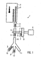
- Fig. 1 shows a schematic view of an apparatus 1 for testing electronic components 3.
- the electronic components 3, such as typically IC chips or the like, can be heated or cooled in a tempering device 2 to a predetermined temperature.
- the tempering device 2 does not have to be used or provided. Testing of the components at room temperature is also possible.
- the device is a gravity handler.
- the path taken by the electronic components is essentially vertical.
- the electronic components 3 are singled out and guided along a guide channel 4 to a transfer element 5.
- suitable separating means may be provided and one or more stoppers for purposefully stopping the various electronic components along the channel.
- the movements of the electronic components is caused by gravity or at least partly caused.
- An electronic component 3 is introduced into the transfer element 5 (eg let it fall through), as shown in FIG Fig. 1 is shown.
- the transfer element 5 can then be brought along the guide 6 in the test position 7.
- Adjacent to the test position 7 is an electrical test head 8, which is actuated by a test device 9 shown schematically. With the electrical test head 8, the electrical Connections of an electronic component 3 can be contacted to test this with respect to its electronic properties.
- the transfer element 5 is moved back from the test position 7 in the Beladeposi- tion (see Fig. 1 ) to eject the tested electronic component 3 downward (eg, by falling out by gravity) and to receive a new electronic component to be tested from above.
- Fig. 1 In the illustration, only one transfer element 5 can be seen, since a second transfer element is covered by the first transfer element.
- various branches may be provided to guide the tested electronic components 3 into one or the other discharge channel or storage 11, 12, 13, depending on the test result.
- Fig. 2 are sectional views at the level of the transfer element 5 in the Fig. 1 shown in plan view. The illustrations are schematic and essentially show the respective loading positions of a transfer element 5a, 5b and the test position 7.
- a first transfer element 5a and a second transfer element 5b are arranged next to one another.
- Each of these two transfer elements can be loaded with electronic components 3 (from above, ie from a direction above the plane of the drawing) and each of these transfer elements can output tested electronic components downwards (in a direction below the drawing plane).
- Each of the two transfer elements 5a, 5b can be transferred separately into the common test position 7 along the paths 14a, 14b.
- the return takes place along the way. However, other ways are possible for the return.
- an intermediate position is provided with the reference numeral 15.
- the transfer element 5a in the position 15 has the same orientation as in the loading position or in the test position 7. From the loading position, the transfer element 5a can be transferred to the position 15 or the position 7 with a pure linear displacement, without a Rotational movement would be superimposed. This means that the orientation is the same in each case.
- Fig. 2b shown that the intermediate position 15 'compared to the loading or test position 7 can also be rotated.
- an embodiment is advantageous in which the orientation of the transfer element 5a, 5b does not change or does not substantially change in comparison to the tangent of the path 14a, 14b, at which the transfer element 5a, 5b is currently located. This facilitates a guide along predetermined guides. Even if in Fig. 2b the intermediate position is rotated, the loading and the test position 7 still has the same orientation.
- the transfer elements 5a, 5b can be guided into the test position 7, but also along rectilinear paths 16a, 16b.
- a corresponding intermediate position is shown at reference numeral 17.
- a distance piece 19 may be provided along which the paths 18a, 18b, which are shown here in dashed lines only schematically in the approach, overlap one above the other. This allows a vertical shrinkage of the transfer elements 5a, 5b on the electrical test head 8. This reduces wear of the electrical contacts of the electrical test head 8, since no dragging transverse movements take place, as for example in FIG Fig. 2c could occur.
- the ways 18a and 18b in Fig. 2d may be rectilinear or curved, curved, curved, S-shaped or otherwise formed.
- Fig. 2e the two loading positions of transfer elements 20a, 20b are not juxtaposed, but arranged opposite one another. From the positions in the Fig. 2a-2d are the in Fig. 2e shown positions by rotation by 90 ° emerged. However, larger or smaller angles of rotation than 90 °, such as 30 °, 45 °, 60 ° or more or less than 30 °, 45 °, or 60 ° are conceivable.
- a transfer element 20a, 20b can be brought into the test position 7 by a pivoting movement. Furthermore, a vertical shrinkage in the test position 7 is guaranteed here.
- the transfer element 20a can be transferred about a pivot axis 22a in the position 7. This is a pure rotational movement without a linear component. The same applies to the transfer element 20b when pivoting about the axis 22b.
- the respective paths are designated 21 a, 21 b.
- FIG. 2f another possible embodiment is shown in which the loading positions of the transfer elements 23a and 23b compared to the positions in Figs. 2a-2d and 2e stand diagonally. From such a position, the transfer of the transfer element 23a, 23b into the test position 7 with a pure rotational movement or as in Fig. 2f shown, with a movement, which are composed of a rectilinear, a curved and a rectilinear motion, achieved. The required rotation angles are compared to Fig. 2e smaller, so the movement can be done faster.
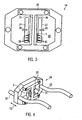
- Fig. 3 a detail view of a transfer element is shown. This bears the reference numeral 24 and corresponds to the transfer elements 5a, 5b, 20a, 20b, 23a, 23b in Fig. 2 ,
- Fig. 4 is a three-dimensional schematic view of the transfer element 24 from Fig. 3 shown schematically.
- the transfer element 24 has a frame around one or two openings 29, to which a double-T-shaped element 25 is attached with a web 31. Between the base body of the transfer element 24 and the web 31, an electronic component to be tested can slide from top to bottom.
- a stopper 27 is provided which can engage the electrical contacts 30 of an electronic component 3 to be tested with corresponding projections (see lower end of the stoppers 27).
- Other stoppers which attack the electronic component to be tested on the body are also possible in addition or as an alternative.
- a stopper and vacuum openings may be provided which hold an electronic component.
- the electronic component 3 can be released so that it can slide down out.
- an insulator material 26 is arranged, which serves to insulate the electrical contacts 30 of the electronic component 3 against the web 31 and to guide the electronic component 3.
- the electronic contacts are accessible from the outside and can be contacted by the contacts of the electrical test head 8.
- a guide of rods 32 is shown by way of example.
- the transfer element 24 can be moved back and forth along these rods 32 in the direction 33.
- an S-shaped guide of the transfer element 24 is possible.
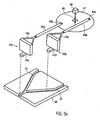
- Fig. 5a a preferred variant for driving the transfer elements is shown.
- the transfer elements have reference numbers 43a and 43b here.
- a plate 40 with grooves 41 and 42 is provided below the transfer elements. This plate 40 is shown here for better graphical representation down along the dashed line as deposed in an exploded view.
- boats 44a, 44b can slide along. These shuttles 44a, 44b may in part be arranged in front of or behind the respective transfer element 43a, 43b or else thereof.
- the boats are advantageously at least as long that they are longer than the common path of the grooves 41, 42 at the in Fig. 5a arranged on the left front common path. This ensures that a boat 44b entering the groove 41 is also returned to this groove. The same applies to the shuttle 44a.
- two separate route guides can be provided. This is made possible, for example, by the fact that the boats do not lie centrally in the transfer elements, but are displaced outwards in each case. This is also advantageous for an output of the tested electronic components, since otherwise a boat could be in the way.
- a holder 45a or 45b is arranged together with a rod 46a, 46b.
- the rods 46a, 46b are connected via pivot points 49a, 49b to a rotatable disk 47.
- the disc 47 can be substantially rotated back and forth, this being done by a motor 49 about an axis 48.
- the motor 49 may be a pneumatic actuator, a stepping motor, a servomotor or other motor.
- connection between the rotatable disk 47 and the transfer elements 43a, 43b can also take place via the shuttles 44a, 44b, in that the rods 46 or the holders 45 engage the shuttles.
- the transfer element 43a By rotating the disc 47 in a clockwise direction by about 150 °, the transfer element 43a is pulled back by the rod 46a, while at the same time the transfer member 43b is pushed by the rod 46 b to the front. As a result, the transfer element 43b is brought into the test position and the transfer element 43a is returned to the left loading position.
- FIG. 5b Another drive form is in Fig. 5b shown.
- a servomotor 52b can reciprocate another servomotor 53b in the direction 55.
- the servo motor 53b can move a carrier 54b in a direction 56 back and forth.
- the transfer elements 63a and 63b are shown in their respective loading position and the view is toward the device in the direction from the electrical test head Fig. 1 directed. In the direction of the drawing plane and shown in dashed lines is the test position 64.
- the loading position supply channels 62a, 62b are shown for the two loading positions. These can be straight and / or independent of each other.
- Fig. 6 an embodiment is shown in which both channels 62a, 62b are served by a common channel 60.
- a switch 61 is shown schematically, can be given with the electronic components to be tested 3 from the channel 60 either in the channel 62 a or in the channel 62 b.
- two channels 66a and 66b are provided here, which can also be formed independently of one another. Preferably, they lead straight down (see also Fig. 1 with channel 10).
- Fig. 6 an embodiment is shown in which the two channels 66a and 66b open into a common channel 67. This allows the use of only one channel with corresponding branches in the containers 11, 12, 13 (see Fig. 1 ). With two independent channels, twice the number of branches is needed, which is more mechanically complicated.
- Fig. 7 shows a possible arrangement of several transfer elements 5 side by side and one above the other.
- Electronic components 3 can be supplied or removed along the channels 70, 71, 72.
- the two transfer elements 5 left in the upper row can be used to serve a common test position, whereas the two right transfer elements in the upper row can be used to serve another test position.
- the respective superimposed transfer elements 5 are advantageously coupled directly or indirectly with each other mechanically so that they are moved together. As a result, it is possible to use two electrical test positions lying one above the other alternately with the transfer elements 5 of the first and second gaps (in FIG Fig. 7 from left). In the Fig. 7 left four transfer elements 5 can be driven by a single motor. The same applies to the four in Fig. 7 right arranged transfer elements 5.
- the electronic components 3 can be conveyed from the respective upper transfer elements 5 through the lower transfer elements 5 to the exit and electronic components to be tested for the respective lower transfer element are passed through the upper transfer element.
- FIG. 8 For example, another example is shown in which a common loading position is provided for two transfer elements 80a, 80b. Between the loading position 88 and the test position 89 two paths 82a and 82b are provided, wherein the transfer element 80b is to be moved along the path 82b and the transfer element 80a along the path 82a (see also FIG Fig. 8b ).
- the drive is similar to in Fig. 5a with a rotary element 87 and two rods 81 a, 81 b, which are each mounted at pivot points 84 a, 84 b.
- the rods engage directly with the transfer elements 80a, 80b, as in FIG Fig. 5a is possible.
- a transfer element 90a is shown in a loading position 92a. In this position, it can be loaded with an electronic component to be tested.
- the other transfer element 90b is located in the common test position 91. There it can be detected by the electrical test head 8 (see Fig. 1 ) be tested.
- the transfer element 90b is transferred from the common test position 91 to the loading position 92b (see FIG Fig. 9b ). In this position, the tested electronic component can be output downwards (see Fig. 1 and 6 ) and loaded with a new component to be tested.
- the transfer member 90a may be transferred from the loading position 92a to the common test position 91. There, the component can then be tested.
- the transfer element 90a is moved back from the common test position 91 back into the loading position 92a (see FIG Fig. 9a ) and during or after that, the transfer member 90b may be transferred from the loading position with the new electronic component to be tested from the loading position 92b to the common test position 91 (see FIG Fig. 9a ). This process can then be repeated to test many components.
Landscapes
- Engineering & Computer Science (AREA)
- Computer Hardware Design (AREA)
- Microelectronics & Electronic Packaging (AREA)
- General Engineering & Computer Science (AREA)
- Physics & Mathematics (AREA)
- General Physics & Mathematics (AREA)
- Testing Of Individual Semiconductor Devices (AREA)
- Testing Electric Properties And Detecting Electric Faults (AREA)
Claims (15)
- Dispositif destiné à tester des composants électroniques (3), comprenant :au moins deux éléments de transfert mécaniques (5a, 5b, 90a, 90b), dont chacun peut être chargé avec un composant électronique (3) respectivement au niveau d'une, qui lui est propre, de deux positions de chargement (92a; 92b) différentes, séparées l'une de l'autre spatialement,caractériséen ce qu'il est prévu une position de test (7) commune pour les composants électroniques (3), dans laquelle peuvent être amenés les deux éléments de transfert (5a, 5b),le dispositif étant conçu de manière à pouvoir déplacer les éléments de transfert (5a, 5b) entre la position de chargement (92a; 92b) et la position de test (7), etles éléments de transfert étant agencés de manière telle, que les composants électroniques puissent tomber dans les éléments de transfert sous l'effet de la gravité, et puissent tomber hors de ceux-ci sous l'effet de la gravité.
- Dispositif selon la revendication 1, caractérisé en ce que la trajectoire des éléments de transfert (5a, 5b) de la position de chargement (5a, 5b) à la position de test (7) est de forme rectiligne (16a, 16b), de forme courbe (14a, 14b, 21a, 12b, 23a, 23b), en forme de S (14a, 14b), ou est constituée de portions rectilignes et de forme courbe.
- Dispositif selon la revendication 1 ou la revendication 2, caractérisé en ce qu'au moins un ou deux éléments de transfert (5a, 5b) présentent la même orientation dans la position de chargement que dans la position de test (7).
- Dispositif selon la revendication 3, caractérisé en ce qu'au moins un ou deux éléments de transfert (5a, 5b) présentent toujours, sur la trajectoire entre la position de chargement et la position de test (7), l'orientation telle que dans la position de chargement et de test.
- Dispositif selon la revendication 3, caractérisé en ce qu'un ou deux éléments de transfert (5a, 5b) présentent, tout au moins sur une ou plusieurs parties de la trajectoire entre la position de chargement et la position de test (7) ou sur l'ensemble de la trajectoire, une orientation tournée par rapport à l'orientation telle que dans la position de chargement et de test (7).
- Dispositif selon l'une des revendications 1 ou 2, caractérisé en ce qu'au moins un ou deux éléments de transfert (20a, 20b, 23a, 23b) présentent une orientation différente dans la position de chargement et dans la position de test.
- Dispositif selon l'une des revendications 1 à 6, caractérisé en ce que les trajectoires entre les deux positions de chargement et la position de test présentent une étendue mutuellement coïncidente au moins dans la zone (19) directement avant la position de test (7).
- Dispositif selon l'une des revendications 1 à 7, caractérisé en ce que les trajectoires pour les éléments de transfert (24, 43a, 43b) entre la position de chargement et la position de test sont prédéterminées par des guidages comme par exemple des tiges (32), des rails, des rainures (41, 42) ou des coulisses.
- Dispositif selon l'une des revendications 1 à 8, caractérisé en ce que les éléments de transfert (50a, 50b) sont déplacés entre la position de chargement et la position de test, respectivement par un entraînement à un, deux ou plusieurs axes (52, 53, 54).
- Dispositif selon l'une des revendications 1 à 9, caractérisé en ce que les deux éléments de transfert (43a, 43b) sont reliés à un moyen d'entraînement (47, 49) commun.
- Dispositif selon la revendication 10, caractérisé en ce que les deux éléments de transfert (43a, 43b) sont reliés au moyen d'entraînement (47, 49) commun, par des éléments de liaison mécaniquement rigides comme par exemple des tiges (46a, 46b) ou des éléments de forme.
- Dispositif selon la revendication 10 ou la revendication 11, caractérisé en ce que le moyen d'entraînement commun comprend un élément rotatif (47) comme par exemple un disque rotatif ou un cylindre rotatif, qui peut être entraîné par voie pneumatique, électrique, hydraulique, à l'aide d'un moteur pas à pas ou d'un servomoteur (49).
- Dispositif selon l'une des revendications 1 à 12, caractérisé en ce que des composants électroniques peuvent être amenés aux deux positions de chargement de manière mutuellement indépendante, ou des composants électroniques sont amenés aux deux positions de chargement par l'intermédiaire d'un canal (60) au moins partiellement commun.
- Dispositif selon l'une des revendications 1 à 13, caractérisé en ce qu'au moins un ou deux éléments de transfert (5) sont couplés respectivement à au moins un autre élément de transfert.
- Procédé pour tester des composants électroniques (3) comprenant les étapes suivantes :un premier élément de transfert est chargé avec un composant électronique, dans une première position de chargement du premier élément de transfert, le composant électronique tombant dans l'élément de transfert sous l'effet de la gravité ;au moins partiellement de manière simultanée, un composant électronique est testé dans un deuxième élément de transfert qui se trouve dans une position de test commune ;après le test du composant électronique du deuxième élément de transfert, celui-ci est amené dans une deuxième position de chargement, qui est différente de la première position de chargement et séparée spatialement de celle-ci, pour l'évacuer vers le bas en le laissant tomber sous l'effet de la gravité ;ensuite, ou au moins partiellement de manière simultanée, le premier élément de transfert est amené à la position de test commune.
Priority Applications (3)
| Application Number | Priority Date | Filing Date | Title |
|---|---|---|---|
| EP06024651.9A EP1832886B1 (fr) | 2006-03-08 | 2006-11-28 | Dispositif et procédé destiné au test de composants électroniques |
| MYPI20070337A MY146701A (en) | 2006-03-08 | 2007-03-05 | Device and method for testing electronic components |
| US11/683,279 US7673520B2 (en) | 2006-03-08 | 2007-03-07 | Device and method for testing electronic components |
Applications Claiming Priority (2)
| Application Number | Priority Date | Filing Date | Title |
|---|---|---|---|
| EP06004765 | 2006-03-08 | ||
| EP06024651.9A EP1832886B1 (fr) | 2006-03-08 | 2006-11-28 | Dispositif et procédé destiné au test de composants électroniques |
Publications (2)
| Publication Number | Publication Date |
|---|---|
| EP1832886A1 EP1832886A1 (fr) | 2007-09-12 |
| EP1832886B1 true EP1832886B1 (fr) | 2015-04-01 |
Family
ID=38370705
Family Applications (1)
| Application Number | Title | Priority Date | Filing Date |
|---|---|---|---|
| EP06024651.9A Not-in-force EP1832886B1 (fr) | 2006-03-08 | 2006-11-28 | Dispositif et procédé destiné au test de composants électroniques |
Country Status (3)
| Country | Link |
|---|---|
| US (1) | US7673520B2 (fr) |
| EP (1) | EP1832886B1 (fr) |
| MY (1) | MY146701A (fr) |
Families Citing this family (3)
| Publication number | Priority date | Publication date | Assignee | Title |
|---|---|---|---|---|
| DE102007047678B4 (de) * | 2007-10-05 | 2010-02-11 | Multitest Elektronische Systeme Gmbh | Handhabungsvorrichtung für elektronische Bauelemente, insbesondere IC's, mit Pneumatikzylinderbewegungseinrichtung zum Verschieben von Plungern |
| US9594111B2 (en) * | 2013-02-27 | 2017-03-14 | Infineon Technologies Ag | Turret handlers and methods of operations thereof |
| DE102014107314B3 (de) * | 2014-05-23 | 2015-10-22 | Multitest Elektronische Systeme Gmbh | Führungs- und Stützglied für eine Vorrichtung zum Prüfen von elektronischen Bauteilen |
Citations (3)
| Publication number | Priority date | Publication date | Assignee | Title |
|---|---|---|---|---|
| DE3634860A1 (de) * | 1986-10-13 | 1988-04-14 | Microhandling Handhabungsgerae | Vorrichtung zum sortieren unter gleichzeitigem wenden (insichdrehen um 180(grad)) von quaderfoermigen bauteilen |
| DE3719148A1 (de) * | 1987-06-09 | 1988-12-29 | Willberg Hans Heinrich | Einrichtung zum pruefen und sortieren von elektronischen bauelementen, insbesondere ics |
| US20030117162A1 (en) * | 2001-12-21 | 2003-06-26 | Watts Stephen M. | Parallel integrated circuit test apparatus and test method |
Family Cites Families (20)
| Publication number | Priority date | Publication date | Assignee | Title |
|---|---|---|---|---|
| US4128174A (en) * | 1977-02-28 | 1978-12-05 | Motorola, Inc. | High-speed integrated circuit handler |
| US4506213A (en) * | 1983-07-18 | 1985-03-19 | Sym-Tek Systems, Inc. | Electronic device handler |
| US4691831A (en) * | 1984-06-25 | 1987-09-08 | Takeda Riken Co., Ltd. | IC test equipment |
| DE3715671A1 (de) * | 1987-05-11 | 1988-11-24 | Ekkehard Ueberreiter | Einrichtung zum pruefen und sortieren von elektronischen bauelementen insbesondere chips mit integrierten schaltungen (ic's) |
| JPH0498167A (ja) * | 1990-08-16 | 1992-03-30 | Tokyo Electron Ltd | Ic検査装置 |
| KR930702085A (ko) * | 1990-09-24 | 1993-09-08 | 레이몬드 지. 트위그 | 전자장치 테스트 처리기 |
| US5184068A (en) * | 1990-09-24 | 1993-02-02 | Symtek Systems, Inc. | Electronic device test handler |
| JP3183591B2 (ja) * | 1993-07-02 | 2001-07-09 | 三菱電機株式会社 | 半導体デバイスのテストシステム、半導体デバイスのテスト方法、半導体デバイス挿抜ステーション及びテスト用チャンバ |
| TW312749B (fr) * | 1994-07-26 | 1997-08-11 | Tokyo Electron Co Ltd | |
| JP3533879B2 (ja) * | 1996-07-15 | 2004-05-31 | セイコーエプソン株式会社 | 部材の受け渡し装置および集積回路デバイスの検査装置 |
| JP3503860B2 (ja) * | 1997-03-18 | 2004-03-08 | 株式会社アドバンテスト | Ic試験方法およびこの方法を実施する装置 |
| JP3339390B2 (ja) * | 1997-11-12 | 2002-10-28 | 株式会社村田製作所 | 電子部品の搬送装置 |
| TW432221B (en) * | 1998-05-29 | 2001-05-01 | Advantest Corp | Tray for electronic device, the transporting apparatus of tray for electronic device and testing apparatus for electronic device |
| US6364089B1 (en) * | 1999-12-10 | 2002-04-02 | National Semiconductor Corporation | Multi-station rotary die handling device |
| JP3792996B2 (ja) * | 2000-06-08 | 2006-07-05 | 株式会社新川 | ダイ及び小物部品の移送装置 |
| US6518745B2 (en) * | 2000-10-10 | 2003-02-11 | Mirae Corporation | Device test handler and method for operating the same |
| KR100392229B1 (ko) * | 2001-01-09 | 2003-07-22 | 미래산업 주식회사 | 반도체 소자 테스트 핸들러의 인덱스헤드 |
| US6831454B2 (en) * | 2003-02-20 | 2004-12-14 | Mirae Corporation | Indexing device in semiconductor device handler and method for operating the same |
| US7183785B2 (en) * | 2004-01-29 | 2007-02-27 | Howard Roberts | Test system and method for reduced index time |
| US7274202B2 (en) * | 2005-10-07 | 2007-09-25 | Verigy (Singapore) Pte. Ltd. | Carousel device, system and method for electronic circuit tester |
-
2006
- 2006-11-28 EP EP06024651.9A patent/EP1832886B1/fr not_active Not-in-force
-
2007
- 2007-03-05 MY MYPI20070337A patent/MY146701A/en unknown
- 2007-03-07 US US11/683,279 patent/US7673520B2/en not_active Expired - Fee Related
Patent Citations (3)
| Publication number | Priority date | Publication date | Assignee | Title |
|---|---|---|---|---|
| DE3634860A1 (de) * | 1986-10-13 | 1988-04-14 | Microhandling Handhabungsgerae | Vorrichtung zum sortieren unter gleichzeitigem wenden (insichdrehen um 180(grad)) von quaderfoermigen bauteilen |
| DE3719148A1 (de) * | 1987-06-09 | 1988-12-29 | Willberg Hans Heinrich | Einrichtung zum pruefen und sortieren von elektronischen bauelementen, insbesondere ics |
| US20030117162A1 (en) * | 2001-12-21 | 2003-06-26 | Watts Stephen M. | Parallel integrated circuit test apparatus and test method |
Also Published As
| Publication number | Publication date |
|---|---|
| MY146701A (en) | 2012-09-14 |
| US7673520B2 (en) | 2010-03-09 |
| EP1832886A1 (fr) | 2007-09-12 |
| US20070212201A1 (en) | 2007-09-13 |
Similar Documents
| Publication | Publication Date | Title |
|---|---|---|
| DE10004193C2 (de) | Trägerhandhabungsvorrichtung für ein IC-Modulhandhabungsgerät sowie Verfahren dafür | |
| EP1678744B1 (fr) | Dispositif et procede de positionnement pour transferer des composants electroniques | |
| DE10133448A1 (de) | Ausrichtungsverfahren und -vorrichtung zum Ausrichten eines Schneidmessers | |
| DE4418142A1 (de) | Vorrichtung und Verfahren zum Umsetzen von Teilen in eine Testeinrichtung | |
| EP2982472A1 (fr) | Système de positionnement | |
| DE2028910B2 (de) | Einrichtung zum Sortieren von elektrischen Schaltungselementen | |
| DE60132908T2 (de) | Prüfsystem in einer leiterplatten-herstellungslinie zum automatischen prüfen von leiterplatten | |
| EP0782175A2 (fr) | Appareil de manipulation d'objets en forme de disque | |
| DE3624416C2 (de) | Vorrichtung zum Werkstückbe- und Entladen einer Presse | |
| EP0204291B1 (fr) | Dispositif à tester et trier des composants électroniques, en particulier des puces intégrées | |
| EP2073620A1 (fr) | Dispositif de transport de substrat pour un automate d'implantation | |
| DE102008010236B4 (de) | Vorrichtung zum Transportieren von Substraten bei einem Bestückautomaten, Bestückungsautomat und Verfahren zum Transportieren von Substraten | |
| DE4015315A1 (de) | Verfahren sowie vorrichtung zum einbringen von bauelementen, insbesondere elektrischen bauelementen, bevorzugt chips in vertiefungen eines gurtes | |
| EP0426798B1 (fr) | Dispositif de manipulation d'objets et son application | |
| DE69532379T2 (de) | Greifkopf für eine bestückungsmaschine | |
| DE3902063C2 (fr) | ||
| DE2341524C2 (de) | Maschine zum Bestücken von bedruckten Leiterplatten | |
| EP1832886A1 (fr) | Dispositif et procédé destiné au test de composants électroniques | |
| DE2209252C2 (de) | Einrichtung zum Ausrichten eines kleinen plattenförmigen, rechteckigen Werkstückes | |
| DE19756900A1 (de) | Testvorrichtung für Halbleiterbauelemente | |
| DE3715671A1 (de) | Einrichtung zum pruefen und sortieren von elektronischen bauelementen insbesondere chips mit integrierten schaltungen (ic's) | |
| CH674504A5 (fr) | ||
| EP4211519B1 (fr) | Dispositifs et procédés pour faire fonctionner au moins deux outils | |
| DE102005061680B3 (de) | Einrichtung und Verfahren zur gleichzeitigen Übertragung einer Mehrzahl von elektronischen Bauteilen | |
| EP4338842B1 (fr) | Procédé d'emballage pour pointes de pipettes ou récipients de réaction médical avec contrôle latéral, dispositif d'emballage et système de moulage par injection |
Legal Events
| Date | Code | Title | Description |
|---|---|---|---|
| PUAI | Public reference made under article 153(3) epc to a published international application that has entered the european phase |
Free format text: ORIGINAL CODE: 0009012 |
|
| AK | Designated contracting states |
Kind code of ref document: A1 Designated state(s): AT BE BG CH CY CZ DE DK EE ES FI FR GB GR HU IE IS IT LI LT LU LV MC NL PL PT RO SE SI SK TR |
|
| AX | Request for extension of the european patent |
Extension state: AL BA HR MK YU |
|
| 17P | Request for examination filed |
Effective date: 20080307 |
|
| 17Q | First examination report despatched |
Effective date: 20080402 |
|
| AKX | Designation fees paid |
Designated state(s): AT BE BG CH CY CZ DE DK EE ES FI FR GB GR HU IE IS IT LI LT LU LV MC NL PL PT RO SE SI SK TR |
|
| GRAP | Despatch of communication of intention to grant a patent |
Free format text: ORIGINAL CODE: EPIDOSNIGR1 |
|
| INTG | Intention to grant announced |
Effective date: 20141009 |
|
| GRAS | Grant fee paid |
Free format text: ORIGINAL CODE: EPIDOSNIGR3 |
|
| GRAA | (expected) grant |
Free format text: ORIGINAL CODE: 0009210 |
|
| AK | Designated contracting states |
Kind code of ref document: B1 Designated state(s): AT BE BG CH CY CZ DE DK EE ES FI FR GB GR HU IE IS IT LI LT LU LV MC NL PL PT RO SE SI SK TR |
|
| REG | Reference to a national code |
Ref country code: GB Ref legal event code: FG4D Free format text: NOT ENGLISH |
|
| REG | Reference to a national code |
Ref country code: CH Ref legal event code: EP |
|
| REG | Reference to a national code |
Ref country code: IE Ref legal event code: FG4D Free format text: LANGUAGE OF EP DOCUMENT: GERMAN |
|
| REG | Reference to a national code |
Ref country code: DE Ref legal event code: R096 Ref document number: 502006014261 Country of ref document: DE Effective date: 20150507 |
|
| REG | Reference to a national code |
Ref country code: AT Ref legal event code: REF Ref document number: 719390 Country of ref document: AT Kind code of ref document: T Effective date: 20150515 |
|
| REG | Reference to a national code |
Ref country code: NL Ref legal event code: VDEP Effective date: 20150401 |
|
| REG | Reference to a national code |
Ref country code: LT Ref legal event code: MG4D |
|
| PG25 | Lapsed in a contracting state [announced via postgrant information from national office to epo] |
Ref country code: NL Free format text: LAPSE BECAUSE OF FAILURE TO SUBMIT A TRANSLATION OF THE DESCRIPTION OR TO PAY THE FEE WITHIN THE PRESCRIBED TIME-LIMIT Effective date: 20150401 |
|
| PG25 | Lapsed in a contracting state [announced via postgrant information from national office to epo] |
Ref country code: PT Free format text: LAPSE BECAUSE OF FAILURE TO SUBMIT A TRANSLATION OF THE DESCRIPTION OR TO PAY THE FEE WITHIN THE PRESCRIBED TIME-LIMIT Effective date: 20150803 Ref country code: FI Free format text: LAPSE BECAUSE OF FAILURE TO SUBMIT A TRANSLATION OF THE DESCRIPTION OR TO PAY THE FEE WITHIN THE PRESCRIBED TIME-LIMIT Effective date: 20150401 Ref country code: CZ Free format text: LAPSE BECAUSE OF FAILURE TO SUBMIT A TRANSLATION OF THE DESCRIPTION OR TO PAY THE FEE WITHIN THE PRESCRIBED TIME-LIMIT Effective date: 20150401 Ref country code: LT Free format text: LAPSE BECAUSE OF FAILURE TO SUBMIT A TRANSLATION OF THE DESCRIPTION OR TO PAY THE FEE WITHIN THE PRESCRIBED TIME-LIMIT Effective date: 20150401 Ref country code: ES Free format text: LAPSE BECAUSE OF FAILURE TO SUBMIT A TRANSLATION OF THE DESCRIPTION OR TO PAY THE FEE WITHIN THE PRESCRIBED TIME-LIMIT Effective date: 20150401 |
|
| REG | Reference to a national code |
Ref country code: FR Ref legal event code: PLFP Year of fee payment: 10 |
|
| PG25 | Lapsed in a contracting state [announced via postgrant information from national office to epo] |
Ref country code: GR Free format text: LAPSE BECAUSE OF FAILURE TO SUBMIT A TRANSLATION OF THE DESCRIPTION OR TO PAY THE FEE WITHIN THE PRESCRIBED TIME-LIMIT Effective date: 20150702 Ref country code: LV Free format text: LAPSE BECAUSE OF FAILURE TO SUBMIT A TRANSLATION OF THE DESCRIPTION OR TO PAY THE FEE WITHIN THE PRESCRIBED TIME-LIMIT Effective date: 20150401 Ref country code: IS Free format text: LAPSE BECAUSE OF FAILURE TO SUBMIT A TRANSLATION OF THE DESCRIPTION OR TO PAY THE FEE WITHIN THE PRESCRIBED TIME-LIMIT Effective date: 20150801 |
|
| REG | Reference to a national code |
Ref country code: DE Ref legal event code: R097 Ref document number: 502006014261 Country of ref document: DE |
|
| PG25 | Lapsed in a contracting state [announced via postgrant information from national office to epo] |
Ref country code: EE Free format text: LAPSE BECAUSE OF FAILURE TO SUBMIT A TRANSLATION OF THE DESCRIPTION OR TO PAY THE FEE WITHIN THE PRESCRIBED TIME-LIMIT Effective date: 20150401 Ref country code: DK Free format text: LAPSE BECAUSE OF FAILURE TO SUBMIT A TRANSLATION OF THE DESCRIPTION OR TO PAY THE FEE WITHIN THE PRESCRIBED TIME-LIMIT Effective date: 20150401 |
|
| PLBE | No opposition filed within time limit |
Free format text: ORIGINAL CODE: 0009261 |
|
| STAA | Information on the status of an ep patent application or granted ep patent |
Free format text: STATUS: NO OPPOSITION FILED WITHIN TIME LIMIT |
|
| PG25 | Lapsed in a contracting state [announced via postgrant information from national office to epo] |
Ref country code: RO Free format text: LAPSE BECAUSE OF NON-PAYMENT OF DUE FEES Effective date: 20150401 Ref country code: PL Free format text: LAPSE BECAUSE OF FAILURE TO SUBMIT A TRANSLATION OF THE DESCRIPTION OR TO PAY THE FEE WITHIN THE PRESCRIBED TIME-LIMIT Effective date: 20150401 Ref country code: SK Free format text: LAPSE BECAUSE OF FAILURE TO SUBMIT A TRANSLATION OF THE DESCRIPTION OR TO PAY THE FEE WITHIN THE PRESCRIBED TIME-LIMIT Effective date: 20150401 |
|
| 26N | No opposition filed |
Effective date: 20160105 |
|
| PG25 | Lapsed in a contracting state [announced via postgrant information from national office to epo] |
Ref country code: SI Free format text: LAPSE BECAUSE OF FAILURE TO SUBMIT A TRANSLATION OF THE DESCRIPTION OR TO PAY THE FEE WITHIN THE PRESCRIBED TIME-LIMIT Effective date: 20150401 |
|
| PG25 | Lapsed in a contracting state [announced via postgrant information from national office to epo] |
Ref country code: MC Free format text: LAPSE BECAUSE OF FAILURE TO SUBMIT A TRANSLATION OF THE DESCRIPTION OR TO PAY THE FEE WITHIN THE PRESCRIBED TIME-LIMIT Effective date: 20150401 Ref country code: LU Free format text: LAPSE BECAUSE OF FAILURE TO SUBMIT A TRANSLATION OF THE DESCRIPTION OR TO PAY THE FEE WITHIN THE PRESCRIBED TIME-LIMIT Effective date: 20151128 |
|
| REG | Reference to a national code |
Ref country code: CH Ref legal event code: PL |
|
| GBPC | Gb: european patent ceased through non-payment of renewal fee |
Effective date: 20151128 |
|
| PG25 | Lapsed in a contracting state [announced via postgrant information from national office to epo] |
Ref country code: LI Free format text: LAPSE BECAUSE OF NON-PAYMENT OF DUE FEES Effective date: 20151130 Ref country code: CH Free format text: LAPSE BECAUSE OF NON-PAYMENT OF DUE FEES Effective date: 20151130 |
|
| REG | Reference to a national code |
Ref country code: IE Ref legal event code: MM4A |
|
| PG25 | Lapsed in a contracting state [announced via postgrant information from national office to epo] |
Ref country code: GB Free format text: LAPSE BECAUSE OF NON-PAYMENT OF DUE FEES Effective date: 20151128 Ref country code: IE Free format text: LAPSE BECAUSE OF NON-PAYMENT OF DUE FEES Effective date: 20151128 |
|
| REG | Reference to a national code |
Ref country code: FR Ref legal event code: PLFP Year of fee payment: 11 |
|
| REG | Reference to a national code |
Ref country code: AT Ref legal event code: MM01 Ref document number: 719390 Country of ref document: AT Kind code of ref document: T Effective date: 20151128 |
|
| PGFP | Annual fee paid to national office [announced via postgrant information from national office to epo] |
Ref country code: FR Payment date: 20161127 Year of fee payment: 11 |
|
| PG25 | Lapsed in a contracting state [announced via postgrant information from national office to epo] |
Ref country code: AT Free format text: LAPSE BECAUSE OF NON-PAYMENT OF DUE FEES Effective date: 20151128 |
|
| PG25 | Lapsed in a contracting state [announced via postgrant information from national office to epo] |
Ref country code: HU Free format text: LAPSE BECAUSE OF FAILURE TO SUBMIT A TRANSLATION OF THE DESCRIPTION OR TO PAY THE FEE WITHIN THE PRESCRIBED TIME-LIMIT; INVALID AB INITIO Effective date: 20061128 Ref country code: BG Free format text: LAPSE BECAUSE OF FAILURE TO SUBMIT A TRANSLATION OF THE DESCRIPTION OR TO PAY THE FEE WITHIN THE PRESCRIBED TIME-LIMIT Effective date: 20150401 |
|
| PG25 | Lapsed in a contracting state [announced via postgrant information from national office to epo] |
Ref country code: SE Free format text: LAPSE BECAUSE OF FAILURE TO SUBMIT A TRANSLATION OF THE DESCRIPTION OR TO PAY THE FEE WITHIN THE PRESCRIBED TIME-LIMIT Effective date: 20150401 Ref country code: CY Free format text: LAPSE BECAUSE OF FAILURE TO SUBMIT A TRANSLATION OF THE DESCRIPTION OR TO PAY THE FEE WITHIN THE PRESCRIBED TIME-LIMIT Effective date: 20150401 |
|
| PG25 | Lapsed in a contracting state [announced via postgrant information from national office to epo] |
Ref country code: BE Free format text: LAPSE BECAUSE OF NON-PAYMENT OF DUE FEES Effective date: 20151130 |
|
| PG25 | Lapsed in a contracting state [announced via postgrant information from national office to epo] |
Ref country code: TR Free format text: LAPSE BECAUSE OF FAILURE TO SUBMIT A TRANSLATION OF THE DESCRIPTION OR TO PAY THE FEE WITHIN THE PRESCRIBED TIME-LIMIT Effective date: 20150401 |
|
| REG | Reference to a national code |
Ref country code: FR Ref legal event code: ST Effective date: 20180731 |
|
| PG25 | Lapsed in a contracting state [announced via postgrant information from national office to epo] |
Ref country code: FR Free format text: LAPSE BECAUSE OF NON-PAYMENT OF DUE FEES Effective date: 20171130 |
|
| PGFP | Annual fee paid to national office [announced via postgrant information from national office to epo] |
Ref country code: DE Payment date: 20181126 Year of fee payment: 13 |
|
| PGFP | Annual fee paid to national office [announced via postgrant information from national office to epo] |
Ref country code: IT Payment date: 20181130 Year of fee payment: 13 |
|
| REG | Reference to a national code |
Ref country code: DE Ref legal event code: R119 Ref document number: 502006014261 Country of ref document: DE |
|
| PG25 | Lapsed in a contracting state [announced via postgrant information from national office to epo] |
Ref country code: DE Free format text: LAPSE BECAUSE OF NON-PAYMENT OF DUE FEES Effective date: 20200603 Ref country code: IT Free format text: LAPSE BECAUSE OF NON-PAYMENT OF DUE FEES Effective date: 20191128 |