EP1833071B1 - Anzeigefilter und Anzeigevorrichtung damit - Google Patents
Anzeigefilter und Anzeigevorrichtung damit Download PDFInfo
- Publication number
- EP1833071B1 EP1833071B1 EP07103136A EP07103136A EP1833071B1 EP 1833071 B1 EP1833071 B1 EP 1833071B1 EP 07103136 A EP07103136 A EP 07103136A EP 07103136 A EP07103136 A EP 07103136A EP 1833071 B1 EP1833071 B1 EP 1833071B1
- Authority
- EP
- European Patent Office
- Prior art keywords
- shielding
- radiation
- filter
- light
- display
- Prior art date
- Legal status (The legal status is an assumption and is not a legal conclusion. Google has not performed a legal analysis and makes no representation as to the accuracy of the status listed.)
- Not-in-force
Links
Images


Classifications
-
- G—PHYSICS
- G02—OPTICS
- G02B—OPTICAL ELEMENTS, SYSTEMS OR APPARATUS
- G02B5/00—Optical elements other than lenses
- G02B5/20—Filters
-
- G—PHYSICS
- G02—OPTICS
- G02B—OPTICAL ELEMENTS, SYSTEMS OR APPARATUS
- G02B1/00—Optical elements characterised by the material of which they are made; Optical coatings for optical elements
- G02B1/10—Optical coatings produced by application to, or surface treatment of, optical elements
-
- G—PHYSICS
- G02—OPTICS
- G02B—OPTICAL ELEMENTS, SYSTEMS OR APPARATUS
- G02B1/00—Optical elements characterised by the material of which they are made; Optical coatings for optical elements
- G02B1/10—Optical coatings produced by application to, or surface treatment of, optical elements
- G02B1/11—Anti-reflection coatings
- G02B1/111—Anti-reflection coatings using layers comprising organic materials
-
- G—PHYSICS
- G02—OPTICS
- G02B—OPTICAL ELEMENTS, SYSTEMS OR APPARATUS
- G02B1/00—Optical elements characterised by the material of which they are made; Optical coatings for optical elements
- G02B1/10—Optical coatings produced by application to, or surface treatment of, optical elements
- G02B1/11—Anti-reflection coatings
- G02B1/113—Anti-reflection coatings using inorganic layer materials only
- G02B1/115—Multilayers
- G02B1/116—Multilayers including electrically conducting layers
-
- G—PHYSICS
- G02—OPTICS
- G02B—OPTICAL ELEMENTS, SYSTEMS OR APPARATUS
- G02B5/00—Optical elements other than lenses
-
- G—PHYSICS
- G02—OPTICS
- G02F—OPTICAL DEVICES OR ARRANGEMENTS FOR THE CONTROL OF LIGHT BY MODIFICATION OF THE OPTICAL PROPERTIES OF THE MEDIA OF THE ELEMENTS INVOLVED THEREIN; NON-LINEAR OPTICS; FREQUENCY-CHANGING OF LIGHT; OPTICAL LOGIC ELEMENTS; OPTICAL ANALOGUE/DIGITAL CONVERTERS
- G02F1/00—Devices or arrangements for the control of the intensity, colour, phase, polarisation or direction of light arriving from an independent light source, e.g. switching, gating or modulating; Non-linear optics
- G02F1/01—Devices or arrangements for the control of the intensity, colour, phase, polarisation or direction of light arriving from an independent light source, e.g. switching, gating or modulating; Non-linear optics for the control of the intensity, phase, polarisation or colour
- G02F1/13—Devices or arrangements for the control of the intensity, colour, phase, polarisation or direction of light arriving from an independent light source, e.g. switching, gating or modulating; Non-linear optics for the control of the intensity, phase, polarisation or colour based on liquid crystals, e.g. single liquid crystal display cells
- G02F1/133—Constructional arrangements; Operation of liquid crystal cells; Circuit arrangements
- G02F1/1333—Constructional arrangements; Manufacturing methods
- G02F1/1335—Structural association of cells with optical devices, e.g. polarisers or reflectors
- G02F1/133509—Filters, e.g. light shielding masks
- G02F1/133512—Light shielding layers, e.g. black matrix
-
- H—ELECTRICITY
- H01—ELECTRIC ELEMENTS
- H01J—ELECTRIC DISCHARGE TUBES OR DISCHARGE LAMPS
- H01J11/00—Gas-filled discharge tubes with alternating current induction of the discharge, e.g. alternating current plasma display panels [AC-PDP]; Gas-filled discharge tubes without any main electrode inside the vessel; Gas-filled discharge tubes with at least one main electrode outside the vessel
- H01J11/10—AC-PDPs with at least one main electrode being out of contact with the plasma
-
- H—ELECTRICITY
- H01—ELECTRIC ELEMENTS
- H01J—ELECTRIC DISCHARGE TUBES OR DISCHARGE LAMPS
- H01J11/00—Gas-filled discharge tubes with alternating current induction of the discharge, e.g. alternating current plasma display panels [AC-PDP]; Gas-filled discharge tubes without any main electrode inside the vessel; Gas-filled discharge tubes with at least one main electrode outside the vessel
- H01J11/20—Constructional details
- H01J11/34—Vessels, containers or parts thereof, e.g. substrates
- H01J11/44—Optical arrangements or shielding arrangements, e.g. filters, black matrices, light reflecting means or electromagnetic shielding means
-
- G—PHYSICS
- G02—OPTICS
- G02F—OPTICAL DEVICES OR ARRANGEMENTS FOR THE CONTROL OF LIGHT BY MODIFICATION OF THE OPTICAL PROPERTIES OF THE MEDIA OF THE ELEMENTS INVOLVED THEREIN; NON-LINEAR OPTICS; FREQUENCY-CHANGING OF LIGHT; OPTICAL LOGIC ELEMENTS; OPTICAL ANALOGUE/DIGITAL CONVERTERS
- G02F1/00—Devices or arrangements for the control of the intensity, colour, phase, polarisation or direction of light arriving from an independent light source, e.g. switching, gating or modulating; Non-linear optics
- G02F1/01—Devices or arrangements for the control of the intensity, colour, phase, polarisation or direction of light arriving from an independent light source, e.g. switching, gating or modulating; Non-linear optics for the control of the intensity, phase, polarisation or colour
- G02F1/13—Devices or arrangements for the control of the intensity, colour, phase, polarisation or direction of light arriving from an independent light source, e.g. switching, gating or modulating; Non-linear optics for the control of the intensity, phase, polarisation or colour based on liquid crystals, e.g. single liquid crystal display cells
- G02F1/133—Constructional arrangements; Operation of liquid crystal cells; Circuit arrangements
- G02F1/1333—Constructional arrangements; Manufacturing methods
- G02F1/133308—Support structures for LCD panels, e.g. frames or bezels
- G02F1/133334—Electromagnetic shields
-
- H—ELECTRICITY
- H01—ELECTRIC ELEMENTS
- H01J—ELECTRIC DISCHARGE TUBES OR DISCHARGE LAMPS
- H01J2211/00—Plasma display panels with alternate current induction of the discharge, e.g. AC-PDPs
- H01J2211/20—Constructional details
- H01J2211/34—Vessels, containers or parts thereof, e.g. substrates
- H01J2211/44—Optical arrangements or shielding arrangements, e.g. filters or lenses
- H01J2211/444—Means for improving contrast or colour purity, e.g. black matrix or light shielding means
-
- H—ELECTRICITY
- H01—ELECTRIC ELEMENTS
- H01J—ELECTRIC DISCHARGE TUBES OR DISCHARGE LAMPS
- H01J2329/00—Electron emission display panels, e.g. field emission display panels
- H01J2329/86—Vessels
- H01J2329/868—Passive shielding means of vessels
- H01J2329/869—Electromagnetic shielding
-
- H—ELECTRICITY
- H01—ELECTRIC ELEMENTS
- H01J—ELECTRIC DISCHARGE TUBES OR DISCHARGE LAMPS
- H01J2329/00—Electron emission display panels, e.g. field emission display panels
- H01J2329/86—Vessels
- H01J2329/89—Optical components structurally combined with the vessel
- H01J2329/892—Anti-reflection, anti-glare, viewing angle and contrast improving means
-
- H—ELECTRICITY
- H10—SEMICONDUCTOR DEVICES; ELECTRIC SOLID-STATE DEVICES NOT OTHERWISE PROVIDED FOR
- H10K—ORGANIC ELECTRIC SOLID-STATE DEVICES
- H10K50/00—Organic light-emitting devices
- H10K50/80—Constructional details
- H10K50/86—Arrangements for improving contrast, e.g. preventing reflection of ambient light
- H10K50/865—Arrangements for improving contrast, e.g. preventing reflection of ambient light comprising light absorbing layers, e.g. light-blocking layers
-
- H—ELECTRICITY
- H10—SEMICONDUCTOR DEVICES; ELECTRIC SOLID-STATE DEVICES NOT OTHERWISE PROVIDED FOR
- H10K—ORGANIC ELECTRIC SOLID-STATE DEVICES
- H10K59/00—Integrated devices, or assemblies of multiple devices, comprising at least one organic light-emitting element covered by group H10K50/00
- H10K59/80—Constructional details
- H10K59/8791—Arrangements for improving contrast, e.g. preventing reflection of ambient light
- H10K59/8792—Arrangements for improving contrast, e.g. preventing reflection of ambient light comprising light absorbing layers, e.g. black layers
Definitions
- the present invention relates to a display filter and a display apparatus including the display filter, and more particularly, to a display filter and a display apparatus including the display filter, which can increase a contrast ratio in a bright room, increase brightness, and have a great electromagnetic (EM) radiation-shielding effect.
- EM electromagnetic
- a method of excessively reducing a transmittance of the filter, and controlling reflection amount of external light in order to increase a contrast ratio in a bright room is used.
- a multi-layered transparent conductive film stacking a conductive mesh film, a metal thin film, and a transparent thin film having a high four to six metal thin films in order to increase the EM radiation-shielding effect is used.
- the greater the number of the metal thin films stacked in the multi-layered transparent conductive film there are the greater the EM radiation-shielding effect is.
- transmittance with regard to visible light is decreased, and therefore, brightness is reduced.
- the greater the number of the metal thin films there are the greater a period of time required for production is, and the higher a unit cost of manufacturing is.
- a display filter and a display apparatus including the display filter which can increase a contrast ratio in a bright room, increase brightness, and have a great EM radiation-shielding effect, are required.
- An aspect of the present invention provides a display filter, which can increase a contrast ratio, increase brightness, and have a great electromagnetic (EM) radiation-shielding effect.
- EM electromagnetic
- An aspect of the present invention also provides a display apparatus including a display filter.
- a display filter including the features of claim 1: a filter base; and an external light-shielding layer formed on a surface of the filter base, wherein the external light-shielding layer includes a base substrate including a transparent resin and light-shielding patterns spaced apart on a surface of the base substrate at predetermined intervals.
- a light shielding pattern includes a conductive material and is formed on the surface of the base substrate in stripe form whereby a stripe has a wedge-shaped section; and an electrode pattern disposed at both ends of the light-shielding pattern to be substantially perpendicular to the light-shielding pattern, thereby connecting the light-shielding pattern, wherein the filter base comprises an electromagnetic (EM) radiation-shielding layer including a multi-layered transparent conductive film formed by alternately stacking a metal thin film and a transparent thin film having a high refractive index.
- EM electromagnetic
- a display apparatus including a display filter.
- the display apparatus used for the present invention can be variously applied to large-size display apparatuses such as PDP apparatuses realizing RGB with lattice-patterned pixels, organic light emitting diode (OLED) apparatuses, liquid crystal display (LCD) apparatuses, field emission display (FED) apparatuses, and the like, small-size mobile display apparatuses such as personal digital assistants (PDAs), display windows of small game devices, display windows of cellular phones, and the like, flexible display apparatuses, and the like.
- PDAs personal digital assistants
- display apparatuses may be efficiently applied to display apparatuses for outdoor applications having a strong external light, and display apparatuses installed indoors of public facilities.
- the present invention is described by using the PDP apparatus and the PDP filter used for the PDP apparatus for convenience of description, but the present
- FIG. 1 is an exploded perspective view illustrating a plasma display panel (PDP) apparatus according to an exemplary embodiment of the present invention.
- a structure of the PDP apparatus 100 according to the exemplary embodiment of the present invention includes a case 110, a cover 150 covering an upper part of the case 110, a driving circuit board 120 received in the case 110, a panel assembly 130 including a discharge cell where a gas discharge phenomenon occurs, and a PDP filter 200, as illustrated in FIG. 1 .
- the PDP filter 200 includes a conductive layer including a material with high conductivity on a transparent substrate, and the conductive layer is grounded to the case 110 via the cover 150. Specifically, electromagnetic (EM) radiation generated from the panel assembly 130 is shielded by the cover 150 and the case 110 which are grounded using the conductive layer of the PDP filter 200, before reaching a viewer.
- EM electromagnetic
- the PDP filter 200 shielding EM radiation, near infrared (NI) radiation, external light, and the like is first described, and the PDP apparatus 100 including the PDP filter 200 and the panel assembly 130 is then described.
- FIG. 2 is a sectional view illustrating a PDP filter according to an exemplary embodiment of the present invention
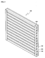
- FIG. 3 is a perspective view illustrating the external light-shielding layer of the PDP filter in FIG. 2 .
- the PDP filter 200 includes a filter base 270 and a color correction layer 240.
- the filter base 270 includes a transparent substrate 210, and layers having various shielding functions, and the like, are disposed on the transparent substrate 210.
- the filter base 270 is formed by stacking the transparent substrate 210, an EM radiation-shielding layer 220, a color correction layer 240, or an antireflective layer 250 regardless of order.
- layers corresponding to an EM radiation-shielding function, a color correction function, and an antireflection function are described as separate layers in the present exemplary embodiment, but the present invention is not limited thereto.
- the filter base 270 according to the present exemplary embodiment may include at least one layer, and each layer may have at least one function from the group consisting of the EM radiation-shielding function, the color correction function, and the antireflection function.
- the filter base 270 may either collectively have the EM radiation-shielding function, the color correction function, and the antireflection function, or have merely one function of the EM radiation-shielding function, the color correction function, and the antireflection function.
- the external light-shielding layer 230 is disposed on a surface of the filter base 270.
- the external light-shielding layer 230 of the exemplary embodiment illustrated in FIG. 2 is disposed on a surface of the filter base 270, i.e. an opposite surface of a viewer position when the PDP filter 200 is installed in the PDP apparatus, but the present invention is not limited thereto, and the external light-shielding layer 230 may be disposed on another surface of the filter base 270.
- the external light-shielding layer 230 includes a supporter 232, a base substrate 234 formed on a surface of the supporter 232, and a light-shielding pattern 236 formed in the base substrate 234.
- the light-shielding pattern 236 shields the panel assembly from external light 320 entering from an outer surface of the PDP filter.
- the light-shielding pattern 236 may be formed in either intaglio or relief in the base substrate 234, and have either a two-dimensional or a three-dimensional shape.
- a wedge-shaped black stripe is described as an example of the light-shielding pattern 236 in the present exemplary embodiment, but the present invention is not limited thereto.
- the base substrate 234 where the light-shielding pattern 236 is formed may be directly formed in the filter base 270, but the base substrate 234 may be combined with the filter base 270 after forming the base substrate 234 on the supporter 232, as illustrated in FIG. 2 .
- the supporter 232 supports the base substrate 234 where the light-shielding pattern 236 is formed.
- the base substrate 234 and the surface of the filter base 270 are combined via the supporter 232 in the exemplary embodiment illustrated in FIG. 2 , but the present invention is not limited thereto.
- the supporter 232 since the supporter 232 has a purpose of supporting the base substrate 234, the base substrate 234 and the filter base 270 may be directly combined when the external light-shielding layer 230 is disposed on another surface of the filter base 270.
- the base substrate 234 may include a compound such as terephthalate, acrylic, polycarbonate, urethane, acrylate, polyester, epoxy acrylate, and acrylate bromide. They are used in alone or in mixture thereof.
- the light-shielding pattern 236 has a section having a wedge-shape, and is formed on the surface of the base substrate 234 corresponding to the panel assembly (not illustrated). Also, the light-shielding pattern 236 prevents the external light 320 from entering an inside of the panel assembly.
- the light-shielding pattern 236 may include at least one material selected from the group consisting of metal, carbon, and a conductive polymeric material.
- the conductive polymeric material includes at least one polymeric material selected from the group consisting of polythiophene, polypyrrole, polyaniline, poly(3,4-ethylenedioxythiophene), poly (3-alkylthiophene), polyisothianaphthene, poly(p-phenylenevinylene), poly(p-phenylene), and a derivative thereof.
- the polymeric material may include at least one material selected from the group consisting of a carbon nanotube, metal powder, and metal oxide powder.
- the light-shielding pattern 236 included in the external light-shielding layer 230 absorbs the external light 320, prevents the external light 320 from entering the panel assembly, and totally reflects the incident light 310 from the panel assembly to the viewer. Accordingly, a high transmittance, with respect to visible light, and a high contrast ratio may be obtained.
- the PDP apparatus has the high transmittance with respect to visible light, and the high contrast ratio.
- the contrast ratio may be shown as Equation 1.
- contrast ratio brightness of white light + reflected light brightness of black light + reflected light Equation 1
- the PDP filter 200 of the present invention uses the light-shielding pattern 236 absorbing light in order to increase the contrast ratio.
- the light-shielding pattern 236 partially absorbs the incident light 310 emitted from the panel assembly, and reduces the brightness of white light and black light by a predetermined portion, thereby increasing the contrast ratio.
- the contrast ratio corresponds to a function with respect to the brightness of reflected light, and reflected light includes light reflected after the external light 320 enters the panel assembly.
- the external light 320 is directly absorbed in the light-shielding pattern 236, or is indirectly absorbed in the light-shielding pattern 236, although reflection occurs in the panel assembly, the brightness of reflected light may be reduced. Accordingly, although identical reflected light with respect to white light and black light is generated, the brightness of reflected light in a denominator of Equation 1 is reduced. Therefore, the contrast ratio may be increased.
- the external light-shielding layer 230 complements the EM radiation-shielding effect.
- the light-shielding pattern 236 included in the external light-shielding layer 230 includes the conductive polymeric material, and may have the EM radiation-shielding effect.
- an EM radiation-shielding loop may be formed by generating an electrode pattern 238 disposed at both ends of the light-shielding pattern 236 being shaped as black stripes to be substantially perpendicular to the light-shielding pattern 236, thereby connecting the light-shielding pattern 236.
- the electrode pattern 238 includes the conductive material.
- the electrode pattern 238 may include the conductive polymeric material, similar to the light-shielding pattern 236.
- the EM radiation-shielding effect of the PDP filter 200 may be increased by the EM radiation-shielding loop.
- the filter base 270 includes the transparent substrate 210, the EM radiation-shielding layer 220 formed on the surface of the transparent substrate 210, and the color correction layer 240 and the antireflective layer 250 formed on the other surface of the transparent substrate 210.
- the present invention is not limited to the above stacking order, and the filter base 270 may have the multi-layered structure regardless of a stacking order of the transparent substrate 210, the EM radiation-shielding layer 220, the color correction layer 240, or the antireflective layer 250.
- a multi-layered transparent conductive film stacking a metal thin film and a transparent thin film having a high refractive index may be used for the EM radiation-shielding layer 220 to have the EM radiation-shielding effect according to the present exemplary embodiment.
- the transparent thin film having the high refractive index such as indium tin oxide (ITO), aluminum zinc oxide (AZO), and the like may be used for the multi-layered transparent conductive film in order to have the EM radiation-shielding effect.
- the transparent thin film having the high refractive index such as indium tin oxide (ITO), aluminum zinc oxide (AZO), and the like
- the metal thin film such as gold, silver, copper, platinum, and palladium
- the transparent thin film having the high refractive index such as indium oxide, stannic oxide, zinc oxide, aluminum oxide, neodymium oxide, and niobium oxide, and the like as the multi-layered transparent conductive film.
- the metal thin film of the multi-layered transparent conductive film may have a high conductivity, and an NI radiation-shielding effect is great by a metal using reflection and absorption extending over a wide wavelength range.
- the transmittance with respect to visible light is relatively low.
- a transparent thin film having the high refractive index of the multi-layered transparent conductive film has a relatively low conductivity or a relatively low reflection effect of NI radiation.
- a transparent thin film having the high refractive index of the multi-layered transparent conductive film has a great transparency.
- the multi-layered transparent conductive film stacking the metal thin film and the transparent thin film having the high refractive index has a characteristic that the conductivity, the NI radiation-shielding effect, and the transmittance with respect to visible light are great by combining advantages of the metal thin film and the transparent thin film having the high refractive index.
- the EM radiation-shielding layer 220 including the one to three multi-layered transparent conductive films being continuously stacked on each other is used in the present exemplary embodiment, a sufficient EM radiation-shielding effect may be obtained.
- the one to three multi-layered transparent conductive films are formed by stacking the metal thin film and the transparent thin film having the high refractive index.
- the conventional EM radiation-shielding layer stacks the four to six metal thin films in order to increase the EM radiation-shielding effect, however, the present exemplary embodiment uses the external light-shielding layer 230 including the light-shielding pattern 236 of the conductive polymeric material.
- the EM radiation-shielding layer 220 including the one to three (more desirably, one to two) multi-layered transparent conductive films being continuously stacked on each other is used, a sufficient EM radiation-shielding effect may be obtained.
- the transparent thin film having the high refractive index may include at least one thin film including the above material, and the metal thin film may also include at least one thin film including the above material.
- various thin films having the EM radiation-shielding effect may be added between the metal thin film and the transparent thin film having the high refractive index.
- EM radiation is shielded by an effect of reflection and absorption of EM radiation by the EM radiation-shielding layer 220.
- a conductive metal thin film is required in the EM radiation-shielding layer 220.
- the conductive metal thin film be thicker than a predetermined value in order to completely absorb EM radiation generated from the display apparatus.
- the thicker the conductive metal thin film is the lower the transmittance with respect to visible light is.
- the multi-layered transparent conductive film alternately stacking the metal thin film and the transparent thin film having the high refractive index may increase a reflective surface and reflection of EM radiation.
- the metal thin film is a thin film layer including either silver or an alloy including silver. Since silver from among silver and the alloy including silver has high conductivity, high reflectivity with respect to infrared radiation, and high transmittance with respect to visible light when stacking multi-layers, it is desirable that silver is used. However, since silver has low chemical and physical stability, and is deteriorated by pollutants of a surrounding environment, vapor, heat, light, and the like, the alloy including silver and at least one other metal which is stable with respect to the surrounding environment, such as gold, platinum, palladium, copper, indium, tin, and the like, may be also used.
- the metal thin film simply formed by silver is used for at least one layer from a plurality of metal thin films forming the multi-layered transparent conductive film.
- the EM radiation-shielding layer 220 having high conductivity and high optical characteristic may be obtained, however, the EM radiation-shielding layer 220 tends to be easily deteriorated by influences of the surrounding environment. This case of silver being deteriorated may be prevented by forming the transparent thin film having the high refractive index on the upper and lower sides of the metal thin film including silver. Any one of conventional well-known methods such as sputtering, ion plating, vacuum deposition, plating, and the like may be used for forming the metal thin film.
- the transparent thin film having the high refractive index has transparency with respect to visible light, and has an effect of preventing the visible light from being reflected by the metal thin film due to a refractive index difference from the metal thin film.
- Specific materials forming the transparent thin film having the high refractive index are an oxide such as indium, titanium, zirconium, bismuth, tin, zinc, antimony, tantalum, cerium, neodymium, lanthanum, thorium, magnesium, potassium, aluminum, niobium, and the like, combinations thereof, zinc sulfide, and the like.
- the oxide or a sulfide has a difference in stoichiometric formation with a metal, oxygen, and sulfur, it is irrelevant in a range by slightly modifying the optical characteristic.
- zinc oxide, a mixture of aluminum oxide and zinc oxide (AZO), indium oxide or a mixture of indium oxide and tin oxide (ITO) from among the oxide and the sulfide has high transparency, a high refractive index, a high growth rate of a film, and a characteristic of adhering closely to the metal thin film, it is desirable that zinc oxide, AZO, indium oxide or ITO is used.
- absorptiveness of EM radiation, and conductivity of the EM radiation-shielding layer 220 may be increased using a thin film of an oxide semiconductor having a relatively high conductivity such as AZO and ITO.
- a thin film of an oxide semiconductor having a relatively high conductivity such as AZO and ITO.
- Any one of conventional well-known methods such as sputtering, ion plating, ion beam assist, vacuum deposition, wet coating, and the like may be used for forming the transparent thin film having the high refractive index.
- the multi-layered transparent conductive film shields NI radiation, when the multi-layered transparent conductive film stacking the metal thin film and the transparent thin film having the high refractive index is used for the EM radiation-shielding layer 220 according to the present exemplary embodiment. Accordingly, two functions corresponding to an NI radiation-shielding function and the EM radiation-shielding function may be simply performed by the EM radiation-shielding layer 220 without separately forming the NI radiation-shielding layer.
- the filter base 270 according to the present exemplary embodiment may separately include an NI radiation-shielding layer.
- the NI radiation-shielding layer is generated from the panel assembly, and shields the strong NI radiation causing electronic devices such as wireless phones, remote controls, and the like, to malfunction.
- Three transparent conductive films are formed on a surface of a transparent substrate by a direct current sputtering method by continuously stacking in an order of a niobium oxide (Nb 2 O 5 ) film corresponding to a transparent thin film having a high refractive index, and a silver thin film corresponding to a metal thin film.
- an EM radiation-shielding layer is formed by stacking the Nb 2 O 5 film on a multi-layered structure of the transparent conductive films.
- the Nb 2 O 5 film is formed using an Nb 2 O 5 target and argon gas as a sputtering gas.
- the silver thin film is formed using a silver target and argon gas as sputtering gas.
- an external light-shielding layer including a light-shielding pattern is formed on the EM radiation-shielding layer.
- the light-shielding pattern has a wedge-shaped black stripe form, and includes the conductive polymeric material.
- a PDP filter is made by forming a color correction layer and an NI radiation-shielding layer on another surface of the transparent substrate. An average transmittance of the PDP filter is controlled to be about 50% in a wavelength range corresponding to about 380 nm to about 780 nm of standard light source D65.
- a PDP filter substantially similar to Experimental example 1 was prepared.
- two multi-layered transparent conductive films being continuously stacked on each other are formed on the transparent substrate, and the EM radiation-shielding layer is formed stacking the Nb 2 O 5 film on the multi-layered transparent conductive films.
- a PDP filter of Comparative experimental example 1 corresponds to the PDP filter, excluding the external light-shielding layer, from Experimental example 1,
- the PDP filter of Comparative experimental example 2 corresponds to the PDP filter, excluding the external light-shielding layer, from Experimental example 2.
- the EM radiation-shielding amount corresponds to a difference of EM radiation values generated from the PDP apparatus in a state where the PDP filter is installed in the panel assembly and a state where the PDP filter is not installed in the panel assembly.
- the EM radiation values are measured according to Class B regulations in a shielded room satisfying American National Standards Institute (ANSI) C63.4-1992 corresponding to a measuring equipment standard for EM radiation.
- ANSI American National Standards Institute
- a display filter and a display apparatus including the display filter, which can increase a contrast ratio, increase brightness, and have an EM radiation-shielding effect of a display apparatus by forming, on the display filter, light-shielding patterns including a conductive polymeric material.
Landscapes
- Physics & Mathematics (AREA)
- General Physics & Mathematics (AREA)
- Optics & Photonics (AREA)
- Engineering & Computer Science (AREA)
- Plasma & Fusion (AREA)
- Chemical & Material Sciences (AREA)
- Nonlinear Science (AREA)
- Electromagnetism (AREA)
- Crystallography & Structural Chemistry (AREA)
- Mathematical Physics (AREA)
- Inorganic Chemistry (AREA)
- Devices For Indicating Variable Information By Combining Individual Elements (AREA)
- Shielding Devices Or Components To Electric Or Magnetic Fields (AREA)
Claims (11)
- Anzeigefilter (200) mit:- einer Filterbasis (270);- einer externen Lichtabschirmschicht (230), die auf einer Oberfläche der Filterbasis (270) ausgebildet ist, wobei die externe Lichtabschirmschicht (230) ein Basissubstrat (234) ausweist, das ein transparentes Harz und Lichtabschirmstrukturen (236) enthält, die auf einer Oberfläche des Basissubstrats in vorgegebenen Abständen angeordnet sind, wobei eine Lichtabschirmstruktur (236) ein leitfähiges Material enthält und in Streifenform auf der Oberfläche des Basissubstrats (234) ausgebildet ist, wodurch der Streifen einen keilförmigen Querschnitt hat; und- eine Elektrodenstruktur (238), die an beiden Enden der Lichtabschirmstruktur (236) so angeordnet ist, dass sie im Wesentlichen senkrecht zur Lichtabschirmstruktur (236) verläuft und dadurch die Lichtabschirmstruktur (236) verbindet,- bei dem die Filterbasis (270) eine Abschirmschicht (220) für elektromagnetische (EM) Strahlung aufweist, die einen mehrlagigen, transparenten, leitfähigen Film enthält, der durch abwechselndes Stapeln einen Metalldünnfilms und eines transparenten Dünnfilms mit einem hohen Brechungsindex gebildet wird.
- Anzeigefilter (200) nach Anspruch 1, bei dem
die EM-Strahlungs-Abschirmschicht (220) einen bis drei mehrlagige, transparente, leitfähige Filme aufweist, die fortlaufend übereinander gestapelt sind. - Anzeigefilter (200) nach Anspruch 1 oder 2, bei dem
die EM-Strahlungs-Abschirmschicht (220) eine mehrlagige Struktur aufweist, in der eine bis drei mehrlagige, transparente, leitfähige Filme durch fortlaufendes Stapeln eines Nioboxidfilms und eines Silberdünnfilms ausgebildet sind, und der Nioboxidfilm auf der mehrlagigen Struktur ausgebildet ist. - Anzeigefilter (200) nach einem der vorigen Ansprüche, bei dem
das Basissubstrat (234) mindestens eine Verbindung aufweist, die aus der Gruppe bestehend aus Terephthalat, Acryl, Polycarbonat, Urethan, Acrylat, Polyester, Epoxyacrylat und Acrylatbromid gewählt wird. - Anzeigefilter (200) nach einem der vorigen Ansprüche, bei dem
die Lichtabschirmstruktur (236) mindestens ein Material aufweist, das aus der Gruppe bestehend aus Metall, Kohlenstoff und einem leitfähigen Polymermaterial gewählt wird. - Anzeigefilter (200) nach Anspruch 5, bei dem
das leitfähige Polymermaterial mindestens ein Polymermaterial aufweist, das aus der Gruppe bestehend aus Polythiophen, Polypyrrol, Polyanilin, Poly(3, 4-Ethylendioxythiophen), Poly(3-Alcyltheophen), Polyisothianaphthen, Poly(p-phenylenvinylen), Poly(p-phenylen) und einem Derivat davon gewählt wird. - Anzeigefilter (200) nach Anspruch 6, bei dem
das Polymermaterial mindestens ein Material aufweist, das aus der Gruppe bestehend aus einem Kohlenstoff-Nanorohr, Metallpulver und Metalloxidpulver gewählt wird. - Anzeigefilter (200) nach Anspruch 1, bei dem
die Elektrodenstruktur (238) ein leitfähiges Polymermaterial aufweist. - Anzeigefilter (200) nach einem der vorigen Ansprüche, bei dem
die Filterbasis (270) mindestens eine Funktion aus der Gruppe bestehend aus EM-Strahlungs-Abschirmfunktion, Farbkorrekturfunktion, Entspiegelungsfunktion und Abschirmfunktion gegen nahe Infrarot- (NI) Strahlung hat. - Anzeigefilter (200) nach einem der vorigen Ansprüche, bei dem
die Filterbasis (270) ein transparentes Substrat (210), die auf einer Oberfläche des transparenten Substrats (210) ausgebildete EM-Strahlungs-Abschirmschicht (220), und eine Farbkorrekturschicht (240) sowie eine auf einer anderen Oberfläche des transparenten Substrats (210) ausgebildete Entspiegelungsschicht (250) aufweist. - Anzeigevorrichtung (100) mit dem Anzeigefilter (200) nach einem der Ansprüche 1 bis 10.
Applications Claiming Priority (1)
| Application Number | Priority Date | Filing Date | Title |
|---|---|---|---|
| KR1020060021845A KR100812345B1 (ko) | 2006-03-08 | 2006-03-08 | 디스플레이 필터 및 이를 포함하는 디스플레이 장치 |
Publications (2)
| Publication Number | Publication Date |
|---|---|
| EP1833071A1 EP1833071A1 (de) | 2007-09-12 |
| EP1833071B1 true EP1833071B1 (de) | 2011-02-09 |
Family
ID=38478320
Family Applications (1)
| Application Number | Title | Priority Date | Filing Date |
|---|---|---|---|
| EP07103136A Not-in-force EP1833071B1 (de) | 2006-03-08 | 2007-02-27 | Anzeigefilter und Anzeigevorrichtung damit |
Country Status (7)
| Country | Link |
|---|---|
| US (2) | US20070210821A1 (de) |
| EP (1) | EP1833071B1 (de) |
| JP (1) | JP4327861B2 (de) |
| KR (1) | KR100812345B1 (de) |
| CN (1) | CN101034172B (de) |
| AT (1) | ATE498196T1 (de) |
| DE (1) | DE602007012376D1 (de) |
Families Citing this family (14)
| Publication number | Priority date | Publication date | Assignee | Title |
|---|---|---|---|---|
| US7852002B2 (en) | 2007-05-03 | 2010-12-14 | Lg Electronics Inc. | Filter and plasma display device thereof |
| KR100973647B1 (ko) * | 2007-11-20 | 2010-08-02 | 삼성코닝정밀소재 주식회사 | 디스플레이 장치용 필터 |
| JP2009133949A (ja) * | 2007-11-29 | 2009-06-18 | Dainippon Printing Co Ltd | プラズマディスプレイ用前面フィルターおよびこれを用いたプラズマディスプレイ |
| US8121452B2 (en) * | 2008-02-20 | 2012-02-21 | Hitachi Cable, Ltd. | Method for fabricating a hollow fiber |
| JP5043732B2 (ja) * | 2008-03-26 | 2012-10-10 | パナソニック株式会社 | ディスプレイ用光学フィルム、ディスプレイ用光学シート体、ディスプレイ装置、及びディスプレイ用光学フィルムの製造方法 |
| US20100079870A1 (en) * | 2008-09-26 | 2010-04-01 | Canon Kabushiki Kaisha | Glare reduction film for display screens |
| JP2010085634A (ja) * | 2008-09-30 | 2010-04-15 | Hitachi Ltd | プラズマディスプレイ装置 |
| KR20110013954A (ko) * | 2009-08-04 | 2011-02-10 | 삼성전자주식회사 | 전자파장애를 방지하는 디스플레이 장치 |
| US10529564B2 (en) * | 2015-08-07 | 2020-01-07 | North Carolina State University | Synthesis and processing of novel phase of boron nitride (Q-BN) |
| KR102514320B1 (ko) * | 2015-12-24 | 2023-03-27 | 삼성디스플레이 주식회사 | 표시 장치 |
| US10419063B2 (en) * | 2016-12-30 | 2019-09-17 | Waviot Integrated Systems, Llc | Method and system for receiving telemetry messages over RF channel |
| KR102423030B1 (ko) * | 2017-06-05 | 2022-07-20 | 삼성디스플레이 주식회사 | 전자 장치 및 이의 제조 방법 |
| KR102901392B1 (ko) * | 2020-01-08 | 2025-12-18 | 삼성디스플레이 주식회사 | 표시 모듈 및 이를 포함하는 폴더블 표시 장치 |
| CN113973487B (zh) * | 2020-07-24 | 2025-11-04 | 广州方邦电子股份有限公司 | 一种屏蔽膜及线路板 |
Family Cites Families (22)
| Publication number | Priority date | Publication date | Assignee | Title |
|---|---|---|---|---|
| JP2000105311A (ja) | 1998-09-29 | 2000-04-11 | Nitto Denko Corp | プラズマディスプレイパネル用フィルター |
| US6490091B1 (en) * | 1999-01-21 | 2002-12-03 | Viratec Thin Films, Inc. | Display panel filter and method of making the same |
| KR100322087B1 (ko) | 1999-04-30 | 2002-02-04 | 김순택 | 외광반사가 저감된 플라즈마 디스플레이 및 그 제조방법 |
| KR100416083B1 (ko) | 1999-11-02 | 2004-01-31 | 삼성에스디아이 주식회사 | 플라즈마 디스플레이 소자 |
| KR20020062974A (ko) | 1999-12-28 | 2002-07-31 | 가부시키가이샤 닛폰 쇼쿠바이 | 복층 재료 |
| JP2003023290A (ja) | 2001-07-09 | 2003-01-24 | Dainippon Printing Co Ltd | 電磁波遮蔽用部材及びその製造方法 |
| JP4170677B2 (ja) * | 2002-06-07 | 2008-10-22 | 大日本印刷株式会社 | 光源装置及びディスプレイ |
| TW200405790A (en) * | 2002-08-08 | 2004-04-01 | Dainippon Printing Co Ltd | Electromagnetic wave shielding sheet |
| KR100581856B1 (ko) * | 2002-11-20 | 2006-05-22 | 삼성에스디아이 주식회사 | 다용도 필터를 구비한 플라즈마 디스플레이 패널 |
| KR20040085765A (ko) * | 2003-04-01 | 2004-10-08 | 엘지전자 주식회사 | 플라즈마 디스플레이 패널용 필름형 전면 필터 |
| KR100926712B1 (ko) * | 2003-05-28 | 2009-11-17 | 엘지전자 주식회사 | 전면 필터와 그의 제조 방법 |
| US20060142412A1 (en) * | 2003-06-04 | 2006-06-29 | Mitsubishi Plastics, Inc. | Transparent gel adhesive agent, transparent gel adhesive sheet, and optical filter for display |
| KR100726747B1 (ko) * | 2003-08-25 | 2007-06-11 | 아사히 가라스 가부시키가이샤 | 전자파 차폐 적층체 및 이를 이용한 디스플레이 장치 |
| KR100665026B1 (ko) * | 2004-05-17 | 2007-01-09 | 삼성코닝 주식회사 | 디스플레이 필터, 이를 포함한 디스플레이 장치 및디스플레이 필터의 제조 방법 |
| KR20060008534A (ko) | 2004-07-21 | 2006-01-27 | 삼성코닝 주식회사 | 신규 블랙 매트릭스, 그 제조방법 및 그를 이용한평판표시소자 및 전자파차폐 필터 |
| KR100780283B1 (ko) | 2004-09-01 | 2007-11-28 | 삼성코닝 주식회사 | 전자파 차폐 필름 및 이의 제조방법 |
| KR100674641B1 (ko) * | 2004-12-06 | 2007-01-26 | 김남평 | 점화 플러그 |
| KR100709985B1 (ko) * | 2005-01-04 | 2007-04-23 | 삼성코닝 주식회사 | 디스플레이 장치용 필터 및 이를 포함한 디스플레이 장치 |
| US7755263B2 (en) * | 2005-05-04 | 2010-07-13 | Samsung Corning Precision Glass Co., Ltd. | External light-shielding layer, filter for display device including the external light-shielding layer and display device including the filter |
| CN101067667A (zh) * | 2006-05-03 | 2007-11-07 | 三星康宁株式会社 | 显示滤光器和具有该显示滤光器的显示装置 |
| KR100964109B1 (ko) * | 2006-09-29 | 2010-06-16 | 삼성코닝정밀소재 주식회사 | 외광 차폐 필름 및 이를 포함하는 디스플레이 필터 |
| JP4698660B2 (ja) * | 2006-12-12 | 2011-06-08 | サムスンコーニング精密素材株式会社 | ディスプレイ装置用外光遮蔽フィルムおよびこの製造方法、これを含むディスプレイ装置用フィルタ |
-
2006
- 2006-03-08 KR KR1020060021845A patent/KR100812345B1/ko not_active Expired - Fee Related
-
2007
- 2007-02-27 EP EP07103136A patent/EP1833071B1/de not_active Not-in-force
- 2007-02-27 AT AT07103136T patent/ATE498196T1/de not_active IP Right Cessation
- 2007-02-27 DE DE602007012376T patent/DE602007012376D1/de active Active
- 2007-03-01 JP JP2007052004A patent/JP4327861B2/ja not_active Expired - Fee Related
- 2007-03-08 US US11/715,438 patent/US20070210821A1/en not_active Abandoned
- 2007-03-08 CN CN2007100056492A patent/CN101034172B/zh not_active Expired - Fee Related
-
2010
- 2010-10-15 US US12/905,648 patent/US8262239B2/en not_active Expired - Fee Related
Also Published As
| Publication number | Publication date |
|---|---|
| JP2007243185A (ja) | 2007-09-20 |
| CN101034172A (zh) | 2007-09-12 |
| KR100812345B1 (ko) | 2008-03-11 |
| US20070210821A1 (en) | 2007-09-13 |
| KR20070091989A (ko) | 2007-09-12 |
| ATE498196T1 (de) | 2011-02-15 |
| DE602007012376D1 (de) | 2011-03-24 |
| JP4327861B2 (ja) | 2009-09-09 |
| EP1833071A1 (de) | 2007-09-12 |
| US20110032620A1 (en) | 2011-02-10 |
| CN101034172B (zh) | 2011-01-19 |
| US8262239B2 (en) | 2012-09-11 |
Similar Documents
| Publication | Publication Date | Title |
|---|---|---|
| EP1833071B1 (de) | Anzeigefilter und Anzeigevorrichtung damit | |
| KR100709985B1 (ko) | 디스플레이 장치용 필터 및 이를 포함한 디스플레이 장치 | |
| KR20090052003A (ko) | 디스플레이 장치용 필터 | |
| JP2006313360A (ja) | 外光遮蔽層、これを含むディスプレイ装置用フィルタ及びこれを含んだディスプレイ装置 | |
| KR101043692B1 (ko) | 디스플레이 장치용 필터 및 이를 포함한 디스플레이 장치 | |
| US20090153989A1 (en) | Optical filter for display device | |
| KR100991320B1 (ko) | 표시장치용 필터 및 그 제조 방법 | |
| CN100504455C (zh) | 外界光屏蔽层、用于包括外界光屏蔽层的显示装置的滤光器以及包括滤光器的显示装置 | |
| US8102104B2 (en) | Front-side filter and plasma display panel device including the front-side filter | |
| KR101049460B1 (ko) | 디스플레이 장치용 필터 및 이를 포함한 디스플레이 장치 | |
| KR20090065094A (ko) | 디스플레이 장치용 광학 부재 및 이를 포함하는 디스플레이장치용 필터 | |
| KR101249297B1 (ko) | 디스플레이 장치용 외광 차폐 필름 및 이를 포함하는디스플레이 장치용 필터 | |
| KR101052527B1 (ko) | 전도성 고분자 필름층을 포함하는 pdp 필터 및 이를포함하는 pdp 장치 | |
| KR20080055335A (ko) | 디스플레이 장치용 외광 차폐 필름, 이의 제조 방법 및이를 포함하는 디스플레이 장치용 필터 | |
| KR101043693B1 (ko) | 디스플레이 장치용 필터 및 이를 포함한 디스플레이 장치 | |
| KR20080065420A (ko) | 디스플레이 장치용 광학 부재 및 이를 포함하는 디스플레이장치용 필터 | |
| KR101072432B1 (ko) | 디스플레이 장치용 광학 필터 및 이를 포함하는 디스플레이장치 | |
| KR20080054204A (ko) | 디스플레이 장치용 복합 필름 및 이를 포함하는 디스플레이장치 | |
| KR20070073447A (ko) | 외광 차폐층의 제조 방법 및 디스플레이 필터의 제조 방법 | |
| KR20100088759A (ko) | 외광차폐필름 및 이를 구비하는 광학필터 | |
| KR20080057625A (ko) | 디스플레이필터용 외광차폐층, 이를 포함하는디스플레이필터 및 이를 포함하는 디스플레이 장치 | |
| KR20080095966A (ko) | 디스플레이 장치용 광학 부재 및 이를 포함한 디스플레이장치용 필터 | |
| KR20090039545A (ko) | 디스플레이 장치용 외광 차폐 필름 | |
| KR20080093720A (ko) | 외광 차폐 부재 및 이를 포함한 디스플레이 장치용 필터 | |
| KR20090005573A (ko) | 디스플레이 장치용 광학 부재 및 이를 포함한 디스플레이장치용 필터 |
Legal Events
| Date | Code | Title | Description |
|---|---|---|---|
| PUAI | Public reference made under article 153(3) epc to a published international application that has entered the european phase |
Free format text: ORIGINAL CODE: 0009012 |
|
| 17P | Request for examination filed |
Effective date: 20070227 |
|
| AK | Designated contracting states |
Kind code of ref document: A1 Designated state(s): AT BE BG CH CY CZ DE DK EE ES FI FR GB GR HU IE IS IT LI LT LU LV MC NL PL PT RO SE SI SK TR |
|
| AX | Request for extension of the european patent |
Extension state: AL BA HR MK YU |
|
| RIN1 | Information on inventor provided before grant (corrected) |
Inventor name: PARK, TAE SOONNO. 333-1904, SIBEOMDAEUNMAEUL WORLD Inventor name: SOHN, IN SUNGNO. 604-503, MUJIGAEMAEUL KUNYOUNG AP Inventor name: JUNG, SANG CHEOLNO. 309-1402, AREUMMAEUL TAEYOUNG |
|
| 17Q | First examination report despatched |
Effective date: 20080114 |
|
| RAP1 | Party data changed (applicant data changed or rights of an application transferred) |
Owner name: SAMSUNG CORNING PRECISION GLASS CO., LTD. |
|
| AKX | Designation fees paid |
Designated state(s): AT BE BG CH CY CZ DE DK EE ES FI FR GB GR HU IE IS IT LI LT LU LV MC NL PL PT RO SE SI SK TR |
|
| GRAP | Despatch of communication of intention to grant a patent |
Free format text: ORIGINAL CODE: EPIDOSNIGR1 |
|
| RAP1 | Party data changed (applicant data changed or rights of an application transferred) |
Owner name: SAMSUNG CORNING PRECISION MATERIALS CO., LTD. |
|
| GRAS | Grant fee paid |
Free format text: ORIGINAL CODE: EPIDOSNIGR3 |
|
| GRAA | (expected) grant |
Free format text: ORIGINAL CODE: 0009210 |
|
| AK | Designated contracting states |
Kind code of ref document: B1 Designated state(s): AT BE BG CH CY CZ DE DK EE ES FI FR GB GR HU IE IS IT LI LT LU LV MC NL PL PT RO SE SI SK TR |
|
| REG | Reference to a national code |
Ref country code: GB Ref legal event code: FG4D |
|
| REG | Reference to a national code |
Ref country code: CH Ref legal event code: EP |
|
| REG | Reference to a national code |
Ref country code: IE Ref legal event code: FG4D |
|
| REF | Corresponds to: |
Ref document number: 602007012376 Country of ref document: DE Date of ref document: 20110324 Kind code of ref document: P |
|
| REG | Reference to a national code |
Ref country code: DE Ref legal event code: R096 Ref document number: 602007012376 Country of ref document: DE Effective date: 20110324 |
|
| REG | Reference to a national code |
Ref country code: NL Ref legal event code: VDEP Effective date: 20110209 |
|
| LTIE | Lt: invalidation of european patent or patent extension |
Effective date: 20110209 |
|
| PG25 | Lapsed in a contracting state [announced via postgrant information from national office to epo] |
Ref country code: GR Free format text: LAPSE BECAUSE OF FAILURE TO SUBMIT A TRANSLATION OF THE DESCRIPTION OR TO PAY THE FEE WITHIN THE PRESCRIBED TIME-LIMIT Effective date: 20110510 Ref country code: ES Free format text: LAPSE BECAUSE OF FAILURE TO SUBMIT A TRANSLATION OF THE DESCRIPTION OR TO PAY THE FEE WITHIN THE PRESCRIBED TIME-LIMIT Effective date: 20110520 Ref country code: LT Free format text: LAPSE BECAUSE OF FAILURE TO SUBMIT A TRANSLATION OF THE DESCRIPTION OR TO PAY THE FEE WITHIN THE PRESCRIBED TIME-LIMIT Effective date: 20110209 Ref country code: LV Free format text: LAPSE BECAUSE OF FAILURE TO SUBMIT A TRANSLATION OF THE DESCRIPTION OR TO PAY THE FEE WITHIN THE PRESCRIBED TIME-LIMIT Effective date: 20110209 Ref country code: SE Free format text: LAPSE BECAUSE OF FAILURE TO SUBMIT A TRANSLATION OF THE DESCRIPTION OR TO PAY THE FEE WITHIN THE PRESCRIBED TIME-LIMIT Effective date: 20110209 Ref country code: PT Free format text: LAPSE BECAUSE OF FAILURE TO SUBMIT A TRANSLATION OF THE DESCRIPTION OR TO PAY THE FEE WITHIN THE PRESCRIBED TIME-LIMIT Effective date: 20110609 |
|
| PG25 | Lapsed in a contracting state [announced via postgrant information from national office to epo] |
Ref country code: BE Free format text: LAPSE BECAUSE OF FAILURE TO SUBMIT A TRANSLATION OF THE DESCRIPTION OR TO PAY THE FEE WITHIN THE PRESCRIBED TIME-LIMIT Effective date: 20110209 Ref country code: CY Free format text: LAPSE BECAUSE OF FAILURE TO SUBMIT A TRANSLATION OF THE DESCRIPTION OR TO PAY THE FEE WITHIN THE PRESCRIBED TIME-LIMIT Effective date: 20110209 Ref country code: AT Free format text: LAPSE BECAUSE OF FAILURE TO SUBMIT A TRANSLATION OF THE DESCRIPTION OR TO PAY THE FEE WITHIN THE PRESCRIBED TIME-LIMIT Effective date: 20110209 Ref country code: SI Free format text: LAPSE BECAUSE OF FAILURE TO SUBMIT A TRANSLATION OF THE DESCRIPTION OR TO PAY THE FEE WITHIN THE PRESCRIBED TIME-LIMIT Effective date: 20110209 Ref country code: BG Free format text: LAPSE BECAUSE OF FAILURE TO SUBMIT A TRANSLATION OF THE DESCRIPTION OR TO PAY THE FEE WITHIN THE PRESCRIBED TIME-LIMIT Effective date: 20110509 Ref country code: NL Free format text: LAPSE BECAUSE OF FAILURE TO SUBMIT A TRANSLATION OF THE DESCRIPTION OR TO PAY THE FEE WITHIN THE PRESCRIBED TIME-LIMIT Effective date: 20110209 Ref country code: FI Free format text: LAPSE BECAUSE OF FAILURE TO SUBMIT A TRANSLATION OF THE DESCRIPTION OR TO PAY THE FEE WITHIN THE PRESCRIBED TIME-LIMIT Effective date: 20110209 Ref country code: PL Free format text: LAPSE BECAUSE OF FAILURE TO SUBMIT A TRANSLATION OF THE DESCRIPTION OR TO PAY THE FEE WITHIN THE PRESCRIBED TIME-LIMIT Effective date: 20110209 |
|
| PG25 | Lapsed in a contracting state [announced via postgrant information from national office to epo] |
Ref country code: MC Free format text: LAPSE BECAUSE OF NON-PAYMENT OF DUE FEES Effective date: 20110228 |
|
| REG | Reference to a national code |
Ref country code: CH Ref legal event code: PL |
|
| PG25 | Lapsed in a contracting state [announced via postgrant information from national office to epo] |
Ref country code: CH Free format text: LAPSE BECAUSE OF NON-PAYMENT OF DUE FEES Effective date: 20110228 Ref country code: DK Free format text: LAPSE BECAUSE OF FAILURE TO SUBMIT A TRANSLATION OF THE DESCRIPTION OR TO PAY THE FEE WITHIN THE PRESCRIBED TIME-LIMIT Effective date: 20110209 Ref country code: EE Free format text: LAPSE BECAUSE OF FAILURE TO SUBMIT A TRANSLATION OF THE DESCRIPTION OR TO PAY THE FEE WITHIN THE PRESCRIBED TIME-LIMIT Effective date: 20110209 Ref country code: LI Free format text: LAPSE BECAUSE OF NON-PAYMENT OF DUE FEES Effective date: 20110228 |
|
| REG | Reference to a national code |
Ref country code: IE Ref legal event code: MM4A |
|
| PG25 | Lapsed in a contracting state [announced via postgrant information from national office to epo] |
Ref country code: CZ Free format text: LAPSE BECAUSE OF FAILURE TO SUBMIT A TRANSLATION OF THE DESCRIPTION OR TO PAY THE FEE WITHIN THE PRESCRIBED TIME-LIMIT Effective date: 20110209 Ref country code: SK Free format text: LAPSE BECAUSE OF FAILURE TO SUBMIT A TRANSLATION OF THE DESCRIPTION OR TO PAY THE FEE WITHIN THE PRESCRIBED TIME-LIMIT Effective date: 20110209 Ref country code: RO Free format text: LAPSE BECAUSE OF FAILURE TO SUBMIT A TRANSLATION OF THE DESCRIPTION OR TO PAY THE FEE WITHIN THE PRESCRIBED TIME-LIMIT Effective date: 20110209 |
|
| PLBE | No opposition filed within time limit |
Free format text: ORIGINAL CODE: 0009261 |
|
| STAA | Information on the status of an ep patent application or granted ep patent |
Free format text: STATUS: NO OPPOSITION FILED WITHIN TIME LIMIT |
|
| 26N | No opposition filed |
Effective date: 20111110 |
|
| PG25 | Lapsed in a contracting state [announced via postgrant information from national office to epo] |
Ref country code: IE Free format text: LAPSE BECAUSE OF NON-PAYMENT OF DUE FEES Effective date: 20110227 |
|
| REG | Reference to a national code |
Ref country code: DE Ref legal event code: R097 Ref document number: 602007012376 Country of ref document: DE Effective date: 20111110 |
|
| PG25 | Lapsed in a contracting state [announced via postgrant information from national office to epo] |
Ref country code: IT Free format text: LAPSE BECAUSE OF FAILURE TO SUBMIT A TRANSLATION OF THE DESCRIPTION OR TO PAY THE FEE WITHIN THE PRESCRIBED TIME-LIMIT Effective date: 20110209 |
|
| PG25 | Lapsed in a contracting state [announced via postgrant information from national office to epo] |
Ref country code: LU Free format text: LAPSE BECAUSE OF NON-PAYMENT OF DUE FEES Effective date: 20110227 |
|
| PG25 | Lapsed in a contracting state [announced via postgrant information from national office to epo] |
Ref country code: IS Free format text: LAPSE BECAUSE OF FAILURE TO SUBMIT A TRANSLATION OF THE DESCRIPTION OR TO PAY THE FEE WITHIN THE PRESCRIBED TIME-LIMIT Effective date: 20110209 |
|
| PG25 | Lapsed in a contracting state [announced via postgrant information from national office to epo] |
Ref country code: TR Free format text: LAPSE BECAUSE OF FAILURE TO SUBMIT A TRANSLATION OF THE DESCRIPTION OR TO PAY THE FEE WITHIN THE PRESCRIBED TIME-LIMIT Effective date: 20110209 |
|
| PG25 | Lapsed in a contracting state [announced via postgrant information from national office to epo] |
Ref country code: HU Free format text: LAPSE BECAUSE OF FAILURE TO SUBMIT A TRANSLATION OF THE DESCRIPTION OR TO PAY THE FEE WITHIN THE PRESCRIBED TIME-LIMIT Effective date: 20110209 |
|
| PGFP | Annual fee paid to national office [announced via postgrant information from national office to epo] |
Ref country code: DE Payment date: 20140122 Year of fee payment: 8 |
|
| PGFP | Annual fee paid to national office [announced via postgrant information from national office to epo] |
Ref country code: FR Payment date: 20140124 Year of fee payment: 8 |
|
| PGFP | Annual fee paid to national office [announced via postgrant information from national office to epo] |
Ref country code: GB Payment date: 20140127 Year of fee payment: 8 |
|
| REG | Reference to a national code |
Ref country code: DE Ref legal event code: R119 Ref document number: 602007012376 Country of ref document: DE |
|
| GBPC | Gb: european patent ceased through non-payment of renewal fee |
Effective date: 20150227 |
|
| REG | Reference to a national code |
Ref country code: FR Ref legal event code: ST Effective date: 20151030 |
|
| PG25 | Lapsed in a contracting state [announced via postgrant information from national office to epo] |
Ref country code: DE Free format text: LAPSE BECAUSE OF NON-PAYMENT OF DUE FEES Effective date: 20150901 Ref country code: GB Free format text: LAPSE BECAUSE OF NON-PAYMENT OF DUE FEES Effective date: 20150227 |
|
| PG25 | Lapsed in a contracting state [announced via postgrant information from national office to epo] |
Ref country code: FR Free format text: LAPSE BECAUSE OF NON-PAYMENT OF DUE FEES Effective date: 20150302 |