EP1833097A1 - Verfahren zur bildung einer licht absorbierenden schicht in einer dünnfilm-solarbatterie auf cis-basis - Google Patents
Verfahren zur bildung einer licht absorbierenden schicht in einer dünnfilm-solarbatterie auf cis-basis Download PDFInfo
- Publication number
- EP1833097A1 EP1833097A1 EP05819563A EP05819563A EP1833097A1 EP 1833097 A1 EP1833097 A1 EP 1833097A1 EP 05819563 A EP05819563 A EP 05819563A EP 05819563 A EP05819563 A EP 05819563A EP 1833097 A1 EP1833097 A1 EP 1833097A1
- Authority
- EP
- European Patent Office
- Prior art keywords
- light absorption
- absorption layer
- work
- cis
- atmosphere
- Prior art date
- Legal status (The legal status is an assumption and is not a legal conclusion. Google has not performed a legal analysis and makes no representation as to the accuracy of the status listed.)
- Withdrawn
Links
Images

Classifications
-
- C—CHEMISTRY; METALLURGY
- C23—COATING METALLIC MATERIAL; COATING MATERIAL WITH METALLIC MATERIAL; CHEMICAL SURFACE TREATMENT; DIFFUSION TREATMENT OF METALLIC MATERIAL; COATING BY VACUUM EVAPORATION, BY SPUTTERING, BY ION IMPLANTATION OR BY CHEMICAL VAPOUR DEPOSITION, IN GENERAL; INHIBITING CORROSION OF METALLIC MATERIAL OR INCRUSTATION IN GENERAL
- C23C—COATING METALLIC MATERIAL; COATING MATERIAL WITH METALLIC MATERIAL; SURFACE TREATMENT OF METALLIC MATERIAL BY DIFFUSION INTO THE SURFACE, BY CHEMICAL CONVERSION OR SUBSTITUTION; COATING BY VACUUM EVAPORATION, BY SPUTTERING, BY ION IMPLANTATION OR BY CHEMICAL VAPOUR DEPOSITION, IN GENERAL
- C23C8/00—Solid state diffusion of only non-metal elements into metallic material surfaces; Chemical surface treatment of metallic material by reaction of the surface with a reactive gas, leaving reaction products of surface material in the coating, e.g. conversion coatings, passivation of metals
- C23C8/06—Solid state diffusion of only non-metal elements into metallic material surfaces; Chemical surface treatment of metallic material by reaction of the surface with a reactive gas, leaving reaction products of surface material in the coating, e.g. conversion coatings, passivation of metals using gases
-
- H—ELECTRICITY
- H10—SEMICONDUCTOR DEVICES; ELECTRIC SOLID-STATE DEVICES NOT OTHERWISE PROVIDED FOR
- H10F—INORGANIC SEMICONDUCTOR DEVICES SENSITIVE TO INFRARED RADIATION, LIGHT, ELECTROMAGNETIC RADIATION OF SHORTER WAVELENGTH OR CORPUSCULAR RADIATION
- H10F19/00—Integrated devices, or assemblies of multiple devices, comprising at least one photovoltaic cell covered by group H10F10/00, e.g. photovoltaic modules
- H10F19/30—Integrated devices, or assemblies of multiple devices, comprising at least one photovoltaic cell covered by group H10F10/00, e.g. photovoltaic modules comprising thin-film photovoltaic cells
-
- C—CHEMISTRY; METALLURGY
- C23—COATING METALLIC MATERIAL; COATING MATERIAL WITH METALLIC MATERIAL; CHEMICAL SURFACE TREATMENT; DIFFUSION TREATMENT OF METALLIC MATERIAL; COATING BY VACUUM EVAPORATION, BY SPUTTERING, BY ION IMPLANTATION OR BY CHEMICAL VAPOUR DEPOSITION, IN GENERAL; INHIBITING CORROSION OF METALLIC MATERIAL OR INCRUSTATION IN GENERAL
- C23C—COATING METALLIC MATERIAL; COATING MATERIAL WITH METALLIC MATERIAL; SURFACE TREATMENT OF METALLIC MATERIAL BY DIFFUSION INTO THE SURFACE, BY CHEMICAL CONVERSION OR SUBSTITUTION; COATING BY VACUUM EVAPORATION, BY SPUTTERING, BY ION IMPLANTATION OR BY CHEMICAL VAPOUR DEPOSITION, IN GENERAL
- C23C10/00—Solid state diffusion of only metal elements or silicon into metallic material surfaces
- C23C10/02—Pretreatment of the material to be coated
-
- C—CHEMISTRY; METALLURGY
- C23—COATING METALLIC MATERIAL; COATING MATERIAL WITH METALLIC MATERIAL; CHEMICAL SURFACE TREATMENT; DIFFUSION TREATMENT OF METALLIC MATERIAL; COATING BY VACUUM EVAPORATION, BY SPUTTERING, BY ION IMPLANTATION OR BY CHEMICAL VAPOUR DEPOSITION, IN GENERAL; INHIBITING CORROSION OF METALLIC MATERIAL OR INCRUSTATION IN GENERAL
- C23C—COATING METALLIC MATERIAL; COATING MATERIAL WITH METALLIC MATERIAL; SURFACE TREATMENT OF METALLIC MATERIAL BY DIFFUSION INTO THE SURFACE, BY CHEMICAL CONVERSION OR SUBSTITUTION; COATING BY VACUUM EVAPORATION, BY SPUTTERING, BY ION IMPLANTATION OR BY CHEMICAL VAPOUR DEPOSITION, IN GENERAL
- C23C12/00—Solid state diffusion of at least one non-metal element other than silicon and at least one metal element or silicon into metallic material surfaces
-
- C—CHEMISTRY; METALLURGY
- C23—COATING METALLIC MATERIAL; COATING MATERIAL WITH METALLIC MATERIAL; CHEMICAL SURFACE TREATMENT; DIFFUSION TREATMENT OF METALLIC MATERIAL; COATING BY VACUUM EVAPORATION, BY SPUTTERING, BY ION IMPLANTATION OR BY CHEMICAL VAPOUR DEPOSITION, IN GENERAL; INHIBITING CORROSION OF METALLIC MATERIAL OR INCRUSTATION IN GENERAL
- C23C—COATING METALLIC MATERIAL; COATING MATERIAL WITH METALLIC MATERIAL; SURFACE TREATMENT OF METALLIC MATERIAL BY DIFFUSION INTO THE SURFACE, BY CHEMICAL CONVERSION OR SUBSTITUTION; COATING BY VACUUM EVAPORATION, BY SPUTTERING, BY ION IMPLANTATION OR BY CHEMICAL VAPOUR DEPOSITION, IN GENERAL
- C23C14/00—Coating by vacuum evaporation, by sputtering or by ion implantation of the coating forming material
- C23C14/58—After-treatment
- C23C14/5846—Reactive treatment
- C23C14/5866—Treatment with sulfur, selenium or tellurium
-
- C—CHEMISTRY; METALLURGY
- C23—COATING METALLIC MATERIAL; COATING MATERIAL WITH METALLIC MATERIAL; CHEMICAL SURFACE TREATMENT; DIFFUSION TREATMENT OF METALLIC MATERIAL; COATING BY VACUUM EVAPORATION, BY SPUTTERING, BY ION IMPLANTATION OR BY CHEMICAL VAPOUR DEPOSITION, IN GENERAL; INHIBITING CORROSION OF METALLIC MATERIAL OR INCRUSTATION IN GENERAL
- C23C—COATING METALLIC MATERIAL; COATING MATERIAL WITH METALLIC MATERIAL; SURFACE TREATMENT OF METALLIC MATERIAL BY DIFFUSION INTO THE SURFACE, BY CHEMICAL CONVERSION OR SUBSTITUTION; COATING BY VACUUM EVAPORATION, BY SPUTTERING, BY ION IMPLANTATION OR BY CHEMICAL VAPOUR DEPOSITION, IN GENERAL
- C23C8/00—Solid state diffusion of only non-metal elements into metallic material surfaces; Chemical surface treatment of metallic material by reaction of the surface with a reactive gas, leaving reaction products of surface material in the coating, e.g. conversion coatings, passivation of metals
- C23C8/02—Pretreatment of the material to be coated
-
- H—ELECTRICITY
- H10—SEMICONDUCTOR DEVICES; ELECTRIC SOLID-STATE DEVICES NOT OTHERWISE PROVIDED FOR
- H10F—INORGANIC SEMICONDUCTOR DEVICES SENSITIVE TO INFRARED RADIATION, LIGHT, ELECTROMAGNETIC RADIATION OF SHORTER WAVELENGTH OR CORPUSCULAR RADIATION
- H10F71/00—Manufacture or treatment of devices covered by this subclass
- H10F71/128—Annealing
-
- H—ELECTRICITY
- H10—SEMICONDUCTOR DEVICES; ELECTRIC SOLID-STATE DEVICES NOT OTHERWISE PROVIDED FOR
- H10F—INORGANIC SEMICONDUCTOR DEVICES SENSITIVE TO INFRARED RADIATION, LIGHT, ELECTROMAGNETIC RADIATION OF SHORTER WAVELENGTH OR CORPUSCULAR RADIATION
- H10F77/00—Constructional details of devices covered by this subclass
- H10F77/10—Semiconductor bodies
- H10F77/12—Active materials
- H10F77/126—Active materials comprising only Group I-III-VI chalcopyrite materials, e.g. CuInSe2, CuGaSe2 or CuInGaSe2 [CIGS]
-
- Y—GENERAL TAGGING OF NEW TECHNOLOGICAL DEVELOPMENTS; GENERAL TAGGING OF CROSS-SECTIONAL TECHNOLOGIES SPANNING OVER SEVERAL SECTIONS OF THE IPC; TECHNICAL SUBJECTS COVERED BY FORMER USPC CROSS-REFERENCE ART COLLECTIONS [XRACs] AND DIGESTS
- Y02—TECHNOLOGIES OR APPLICATIONS FOR MITIGATION OR ADAPTATION AGAINST CLIMATE CHANGE
- Y02E—REDUCTION OF GREENHOUSE GAS [GHG] EMISSIONS, RELATED TO ENERGY GENERATION, TRANSMISSION OR DISTRIBUTION
- Y02E10/00—Energy generation through renewable energy sources
- Y02E10/50—Photovoltaic [PV] energy
- Y02E10/541—CuInSe2 material PV cells
-
- Y—GENERAL TAGGING OF NEW TECHNOLOGICAL DEVELOPMENTS; GENERAL TAGGING OF CROSS-SECTIONAL TECHNOLOGIES SPANNING OVER SEVERAL SECTIONS OF THE IPC; TECHNICAL SUBJECTS COVERED BY FORMER USPC CROSS-REFERENCE ART COLLECTIONS [XRACs] AND DIGESTS
- Y02—TECHNOLOGIES OR APPLICATIONS FOR MITIGATION OR ADAPTATION AGAINST CLIMATE CHANGE
- Y02P—CLIMATE CHANGE MITIGATION TECHNOLOGIES IN THE PRODUCTION OR PROCESSING OF GOODS
- Y02P70/00—Climate change mitigation technologies in the production process for final industrial or consumer products
- Y02P70/50—Manufacturing or production processes characterised by the final manufactured product
Definitions
- the present invention relates to a method for forming the light absorption layer of a CIS type thin-film solar cell.
- a CIS type thin-film solar cell is a pn heterojunction device having a substrate structure comprising a glass substrate, a metal back electrode layer, a p-type CIS light absorption layer, a high-resistance buffer layer, and an n-type window layer which have been superposed in this order, as shown in Fig. 7.
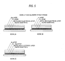
- a metallic precursor film of a multilayer structure comprising any one of Cu/Ga (work 2A), Cu/In (work 2B), and Cu-Ga/In (work 2C) as shown in Fig.
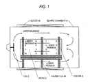
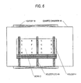
- a method of film formation which has been used for selenizing or sulfurizing the work to be treated for film formation comprises disposing such works in a plate form apart from each other at a certain distance in a cylindrical quartz chamber 1A as shown in Fig. 6 and selenizing or sulfurizing the works based on natural circulation to form light absorption layers.
- the works metal precursor films
- an inert gas e.g., nitrogen gas.
- a selenium source is introduced and heated in the state of being enclosed, and the works are held at a certain temperature for a certain time period to thereby form selenide-based CIS light absorption layers.
- the works are disposed in the apparatus and the atmosphere in the apparatus is replaced with an inert gas, e.g., nitrogen gas. Thereafter, a sulfur source, e.g., sulfide gas, is introduced and heated in the state of being enclosed, and the works are held at a certain temperature for a certain time period to thereby form sulfide-based CIS light absorption layers.
- an inert gas e.g., nitrogen gas.
- the selenium atmosphere enclosed in the apparatus is replaced with a sulfur atmosphere.
- the temperature in the apparatus is elevated while maintaining the sulfur atmosphere and the works are held at a certain temperature for a certain time period to react the works with pyrolytic sulfur and thereby form sulfide/selenide-based CIS light absorption layers.
- the related-art method of film formation (selenization or sulfurization apparatus) based on natural circulation shown in Fig. 6 has had the following problems. Since there is a difference in specific gravity between the reactant gas such as H 2 Se or H 2 S (and chalcogen element (selenium or sulfur)) and a diluent gas (inert gas), the reactant gas is apt to accumulate in a lower part of the reaction furnace and the reactant gas in the furnace becomes uneven. As a result, a light absorption layer in which the proportions of components are uneven is formed, resulting in uneven solar cell performances.
- the reactant gas such as H 2 Se or H 2 S (and chalcogen element (selenium or sulfur)
- a diluent gas ininert gas
- the performances of a solar cell are adversely influenced by any defective part in the work treated for film formation (in the case where given quality or performance is not satisfied) and the presence of such a defective part disadvantageously results in the fabrication of a solar cell which as a whole has poor quality or performances.
- a technique for evenly dispersing a reactant gas in the furnace which comprises disposing a device for evenly dispersing a reactant gas in the furnace, e.g., a fan for stirring the reactant gas, and baffles serving as circulating passages for the reactant gas in a step for fabricating a plasma display panel or the like (see patent document 1).
- the application of this furnace is in the burning of a substrate glass for plasma display panels or the like, and the technique is intended to make the temperature in the furnace even.
- the work in this application differs and no reactant gas is used. Because of this, it is difficult to directly use this technique for the formation of the light absorption layer of a CIS type thin-film solar cell.
- the furnace described in patent document 1 which is a furnace having therein baffles serving as the circulating passages, has a complicated constitution and is expensive. Use of the technique hence has had a problem that production cost increases.
- Patent Document 1 JP-A-11-311484
- An object of the invention is to make the temperature in an apparatus even and improve the state of being in contact with a reactant gas and a chalcogen element (selenium or sulfur) by employing a constitution including (addition of) a simple device and to thereby enable light absorption layers which are simultaneously formed to have even and improved quality (component proportion) and performances and give solar cells with improved performances in improved product yield.
- the invention employs an atmosphere-homogenizing device for making the temperature in the apparatus even and for improving the state of being in contact with reactant gases and chalcogen elements (selenium and sulfur) and the manner of work disposition which enables a reactant gas to circulate smoothly.
- an atmosphere-homogenizing device for making the temperature in the apparatus even and for improving the state of being in contact with reactant gases and chalcogen elements (selenium and sulfur) and the manner of work disposition which enables a reactant gas to circulate smoothly.
- the temperature in the apparatus is made even and the state of being in contact with the reactant gas and a chalcogen element (selenium and sulfur) is improved.
- the light absorption layers of CIS type thin-film solar cells which are simultaneously formed can be made to have even and improved quality (component proportion) and performances.
- the solar cell performances of CIS type thin-film solar cells and the yield of the products can be improved.
- a CIS type thin-film solar cell 5 is a pn heterojunction device of a substrate structure comprising a glass substrate 5A, a metal back electrode layer 5B, a p-type CIS light absorption layer 5C, a high-resistance buffer layer 5D, and an n-type window layer (transparent conductive film) 5E which have been superposed in this order.
- a metallic precursor film of a multilayer structure comprising any one of Cu/Ga (work 2A), Cu/In (work 2B), and Cu-Ga/In (work 2C) as shown in Fig. 5 on a metal back electrode layer 5B on a glass substrate is subjected to the step of film formation by selenization, sulfurization, or selenization/sulfurization to form the CIS light absorption layer 5C.
- forced circulation is employed. Because of this, the invention can eliminate the phenomenon in which a reactant gas such as H 2 Se or H 2 S (and chalcogen element (selenium or sulfur)) is apt to accumulate in a lower part of the reaction furnace due to a difference in specific gravity between the reactant gas and a diluent gas (inert gas) to cause unevenness in reactant gas concentration in the furnace (see the experimental data for a related-art apparatus given in Table 2) and the phenomenon in which an upper part and lower part of the furnace come to have a temperature difference (see the experimental data for a related-art method of film formation give in Fig. 6) ; these phenomena are problems of the related-art method of film formation employing natural circulation.
- a reactant gas such as H 2 Se or H 2 S (and chalcogen element (selenium or sulfur)
- the temperature in the apparatus is made even and the state of being in contact with the reactant gas and chalcogen element (selenium or sulfur) is improved.
- the light absorption layers of CIS type thin-film solar cells which are simultaneously formed can be made to have even and improved quality (component proportion) and performances.
- the solar cell performances of CIS type thin-film solar cells and the yield of the products can be improved.
- a device for atmosphere homogenization is disposed in the apparatus for each step in order to homogenize the temperature and reactant gas in the apparatus and to improve the state of being in contact with the reactant gas and chalcogen element (selenium or sulfur).
- the manner of work disposition is employed in each step in order to make the circulation of the reactant gas smooth.
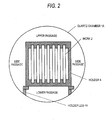
- the device for atmosphere homogenization may be an electric fan 3 and the manner of work disposition may be as follows.
- a holder 4 is used to dispose two or more flat platy works (a group of works) in a cylindrical apparatus (quartz chamber 1A) so that the works 2 are apart from each other at a certain distance and are parallel to the direction of the major axis of the apparatus while keeping the plates vertical, and that the apparatus has inner passages which are reactant-gas passages in the upward/downward direction and the major-axis direction within the group of works and further has an upper passage, a lower passage, and left and right side passages as passages outside the group of works. Furthermore, the device and the manner of disposition enable each work to easily come into contact with the reactant gas present in the apparatus.
- the selenization step may comprise introducing the selenium source, heating the selenium source while keeping it in the state of being enclosed, preparing the inside of the apparatus by the device for atmosphere homogenization and manner of work disposition described above to enable the work to evenly undergo a selenization reaction, and holding each metallic precursor film at a certain temperature for a certain time period to thereby form a selenide-based CIS light absorption layer.
- the selenization step may comprise disposing the work in the apparatus, replacing the atmosphere in the apparatus with an inert gas, e.g., nitrogen gas, subsequently introducing at ordinary temperature a selenium source, e.g., hydrogen selenide gas, diluted to a concentration in the range of 1-20%, desirably 2-10%, homogenizing the gas atmosphere which tends to separate into an upper part and a lower part within the apparatus due to a difference in specific gravity between the gases by the device for atmosphere homogenization and manner of work disposition described above while keeping the selenium source in the state of being enclosed, heating the gas atmosphere to 400-550°C, desirably 450-500°C, at 10-100 °C/min, and thereafter holding the work at this temperature for a certain time period, i.e., 10-200 minutes, desirably 30-120 minutes, to thereby form a selenide-based CIS light absorption layer.
- an inert gas e.g., nitrogen gas
- a selenium source
- the selenide-based CIS light absorption layer may comprise CuInSe 2, Cu (InGa) Se 2, or CuGaSe 2.
- the sulfurization step may comprise disposing the work in an apparatus, replacing the atmosphere in the apparatus with an inert gas, e.g., nitrogen gas, subsequently introducing at ordinary temperature a sulfur source, e.g., sulfide gas, diluted to a concentration in the range of 1-30%, desirably 2-20%, homogenizing the gas atmosphere which tends to separate into an upper part and a lower part within the apparatus due to a difference in specific gravity between the gases by the device for atmosphere homogenization and manner of work disposition described above while keeping the sulfur source in the state of being enclosed, heating the gas atmosphere to 400-550°C, desirably 450-550°C, at 10-100 °C/min, and thereafter holding the work at this temperature for a certain time period, i.e., 10-200 minutes, desirably 30-120 minutes, to thereby form a sulfide-based CIS light absorption layer.
- an inert gas e.g., nitrogen gas
- a sulfur source e.g.
- the sulfide-based CIS light absorption layer may comprise CuInS 2 , Cu(InGa)S 2 , or CuGaS 2 .
- the selenization/sulfurization step may comprise forming the selenide-based CIS light absorption layer described above, thereafter replacing the selenium atmosphere enclosed in the apparatus with a sulfur atmosphere, preparing the inside of the apparatus by the device for atmosphere homogenization described above to enable a sulfurization reaction to proceed evenly while elevating the temperature in the apparatus and maintaining the sulfur atmosphere, and holding the selenide-based CIS light absorption layer at a certain temperature for a certain time period to react the layer with sulfur and thereby form a sulfide/selenide-based CIS light absorption layer.
- the sulfide/selenide-based CIS light absorption layer may comprise CuInSe 2 having CuIn(SSe) 2 or Cu(InGa)(SSe) 2 or CuGa (SSe) 2 or CuIn (SSe) 2 as a surface layer, Cu (InGa) Se 2 having CuIn (SSe) 2 as a surface layer, Cu (InGa) (SSe) 2 having CuIn (SSe) 2 as a surface layer, CuGaSe 2 having CuIn (SSe) 2 as a surface layer, CuGaSe 2 having CuIn (SSe) 2 as a surface layer, Cu (InGa) Se 2 having Cu (InGa) (SSe) 2 as a surface layer, CuGaSe 2 having Cu (InGa) (SSe) 2 as a surface layer, Cu (InGa) Se 2 having CuGa) (SSe) 2 as a surface layer, Cu (InGa) Se 2 having CuGa) (SSe) 2 as a surface layer,
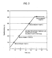
- Fig. 4 shows a comparison between temperature distributions in a work (substrate size: 300 mm x 1,200 mm) in the method of film formation of the invention, which employs the forced circulation, and temperature distributions in a work (substrate size: same as in the invention) in the related-art method of film formation employing natural circulation.
- a film was formed while regulating the temperature in the manner shown in Fig. 3 (heating from room temperature to 510°C at 10 °C/min and holding at 510°C for 30 minutes).
- a thermocouple was attached to each of four sites I, II, III, and IV on the work, and this work was heated according to the temperature program.
- a temperature distribution was determined at each of measurement point A (100°C),measurementpointB (200°C), measurementpointC (400°C), and measurement point D (510°C), and the results thereof are shown.
- the method of film formation of the invention was found to have smaller temperature differences in the work at each measurement point than the related-art method of film formation.
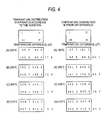
- a CIS type thin-film solar cell (size: 300 mm x 1,200 mm) having a CIS light absorption layer formed by the method of film formation of the invention, which employs the forced circulation, was divided into sixteen pieces (A to P), and each piece was examined for conversion efficiency. The results thereof are shown in Table 1 below (the conversion efficiencies respectively corresponding to the measurement areas A to P are shown).
- a CIS type thin-film solar cell (size: 300 mm x 1,200 mm) having a CIS light absorption layer formed by the related-art method of film formation employing natural circulation was divided into sixteen pieces (A to P), and each piece was examined for conversion efficiency. The results thereof are shown in Table 2 below (the conversion efficiencies respectively corresponding to the measurement areas A to P are shown).
- the conversion efficiencies were determined through a measurement made with a constant-light solar simulator under standard conditions (irradiation intensity, 100 mW/cm 2 ; AM (air mass), 1.5; temperature, 25°C) in accordance with JIS C 8914I.
- the method of film formation of the invention proved to enable a work to have an even temperature distribution throughout the sites therein as shown in Fig. 3 and give a solar cell having an even and high conversion efficiency throughout the sites therein as shown in Table 1.
Landscapes
- Chemical & Material Sciences (AREA)
- Chemical Kinetics & Catalysis (AREA)
- Engineering & Computer Science (AREA)
- Materials Engineering (AREA)
- Mechanical Engineering (AREA)
- Metallurgy (AREA)
- Organic Chemistry (AREA)
- Photovoltaic Devices (AREA)
Applications Claiming Priority (2)
| Application Number | Priority Date | Filing Date | Title |
|---|---|---|---|
| JP2004378398A JP4131965B2 (ja) | 2004-12-28 | 2004-12-28 | Cis系薄膜太陽電池の光吸収層の作製方法 |
| PCT/JP2005/023791 WO2006070745A1 (ja) | 2004-12-28 | 2005-12-26 | Cis系薄膜太陽電池の光吸収層の作製方法 |
Publications (2)
| Publication Number | Publication Date |
|---|---|
| EP1833097A1 true EP1833097A1 (de) | 2007-09-12 |
| EP1833097A4 EP1833097A4 (de) | 2017-03-29 |
Family
ID=36614862
Family Applications (1)
| Application Number | Title | Priority Date | Filing Date |
|---|---|---|---|
| EP05819563.7A Withdrawn EP1833097A4 (de) | 2004-12-28 | 2005-12-26 | Verfahren zur bildung einer licht absorbierenden schicht in einer dünnfilm-solarbatterie auf cis-basis |
Country Status (6)
| Country | Link |
|---|---|
| US (1) | US20080110495A1 (de) |
| EP (1) | EP1833097A4 (de) |
| JP (1) | JP4131965B2 (de) |
| KR (1) | KR101193034B1 (de) |
| CN (1) | CN100490184C (de) |
| WO (1) | WO2006070745A1 (de) |
Cited By (5)
| Publication number | Priority date | Publication date | Assignee | Title |
|---|---|---|---|---|
| EP2319954A1 (de) * | 2009-09-28 | 2011-05-11 | Stion Corporation | Verfahren zur Herstellung von CIS- und/oder CIGS-Dünnfilmen auf Glassubstraten |
| WO2011104231A1 (de) * | 2010-02-23 | 2011-09-01 | Saint Gobain Glass France | Einrichtung zum ausbilden eines reduzierten kammerraums, sowie verfahren zum positionieren von mehrschichtkörpern |
| WO2011104222A1 (de) * | 2010-02-23 | 2011-09-01 | Saint Gobain Glass France | Anordnung, anlage und verfahren zur prozessierung von mehrschichtkörpern |
| EP2144296B1 (de) * | 2008-06-20 | 2014-04-02 | Volker Probst | Verfahren zum Herstellen einer Halbleiterschicht |
| US9284641B2 (en) | 2008-11-28 | 2016-03-15 | Volker Probst | Processing device for producing semiconductor layers and coated substrates treated with elemental selenium and/or sulphur |
Families Citing this family (72)
| Publication number | Priority date | Publication date | Assignee | Title |
|---|---|---|---|---|
| US8017860B2 (en) * | 2006-05-15 | 2011-09-13 | Stion Corporation | Method and structure for thin film photovoltaic materials using bulk semiconductor materials |
| US9105776B2 (en) * | 2006-05-15 | 2015-08-11 | Stion Corporation | Method and structure for thin film photovoltaic materials using semiconductor materials |
| US8414961B1 (en) * | 2006-12-13 | 2013-04-09 | Nanosolar, Inc. | Solution deposited transparent conductors |
| US20080300918A1 (en) * | 2007-05-29 | 2008-12-04 | Commercenet Consortium, Inc. | System and method for facilitating hospital scheduling and support |
| KR100871541B1 (ko) * | 2007-06-26 | 2008-12-05 | 주식회사 동부하이텍 | 이미지센서 및 그 제조방법 |
| US8071179B2 (en) | 2007-06-29 | 2011-12-06 | Stion Corporation | Methods for infusing one or more materials into nano-voids if nanoporous or nanostructured materials |
| US7919400B2 (en) * | 2007-07-10 | 2011-04-05 | Stion Corporation | Methods for doping nanostructured materials and nanostructured thin films |
| WO2009017172A1 (ja) * | 2007-08-02 | 2009-02-05 | Showa Shell Sekiyu K. K. | Cis系薄膜太陽電池の光吸収層の作製方法 |
| US8058092B2 (en) | 2007-09-28 | 2011-11-15 | Stion Corporation | Method and material for processing iron disilicide for photovoltaic application |
| US20090087939A1 (en) * | 2007-09-28 | 2009-04-02 | Stion Corporation | Column structure thin film material using metal oxide bearing semiconductor material for solar cell devices |
| US8759671B2 (en) | 2007-09-28 | 2014-06-24 | Stion Corporation | Thin film metal oxide bearing semiconductor material for single junction solar cell devices |
| US8287942B1 (en) | 2007-09-28 | 2012-10-16 | Stion Corporation | Method for manufacture of semiconductor bearing thin film material |
| US8614396B2 (en) * | 2007-09-28 | 2013-12-24 | Stion Corporation | Method and material for purifying iron disilicide for photovoltaic application |
| US7998762B1 (en) | 2007-11-14 | 2011-08-16 | Stion Corporation | Method and system for large scale manufacture of thin film photovoltaic devices using multi-chamber configuration |
| US8319094B2 (en) | 2007-11-16 | 2012-11-27 | E I Du Pont De Nemours And Company | Multilayer terionomer encapsulant layers and solar cell laminates comprising the same |
| US20090305449A1 (en) * | 2007-12-06 | 2009-12-10 | Brent Bollman | Methods and Devices For Processing A Precursor Layer In a Group VIA Environment |
| ES2409947B1 (es) | 2008-04-17 | 2014-04-29 | Honda Motor Co., Ltd. | Aparato de tratamiento de calor para células solares. |
| US8642138B2 (en) | 2008-06-11 | 2014-02-04 | Stion Corporation | Processing method for cleaning sulfur entities of contact regions |
| US9087943B2 (en) | 2008-06-25 | 2015-07-21 | Stion Corporation | High efficiency photovoltaic cell and manufacturing method free of metal disulfide barrier material |
| US8003432B2 (en) | 2008-06-25 | 2011-08-23 | Stion Corporation | Consumable adhesive layer for thin film photovoltaic material |
| US7855089B2 (en) | 2008-09-10 | 2010-12-21 | Stion Corporation | Application specific solar cell and method for manufacture using thin film photovoltaic materials |
| US8026122B1 (en) | 2008-09-29 | 2011-09-27 | Stion Corporation | Metal species surface treatment of thin film photovoltaic cell and manufacturing method |
| US8501521B1 (en) | 2008-09-29 | 2013-08-06 | Stion Corporation | Copper species surface treatment of thin film photovoltaic cell and manufacturing method |
| US8008112B1 (en) | 2008-09-29 | 2011-08-30 | Stion Corporation | Bulk chloride species treatment of thin film photovoltaic cell and manufacturing method |
| US8394662B1 (en) | 2008-09-29 | 2013-03-12 | Stion Corporation | Chloride species surface treatment of thin film photovoltaic cell and manufacturing method |
| US8236597B1 (en) | 2008-09-29 | 2012-08-07 | Stion Corporation | Bulk metal species treatment of thin film photovoltaic cell and manufacturing method |
| US8476104B1 (en) | 2008-09-29 | 2013-07-02 | Stion Corporation | Sodium species surface treatment of thin film photovoltaic cell and manufacturing method |
| US8008110B1 (en) | 2008-09-29 | 2011-08-30 | Stion Corporation | Bulk sodium species treatment of thin film photovoltaic cell and manufacturing method |
| US7863074B2 (en) | 2008-09-30 | 2011-01-04 | Stion Corporation | Patterning electrode materials free from berm structures for thin film photovoltaic cells |
| US8008198B1 (en) * | 2008-09-30 | 2011-08-30 | Stion Corporation | Large scale method and furnace system for selenization of thin film photovoltaic materials |
| US7947524B2 (en) | 2008-09-30 | 2011-05-24 | Stion Corporation | Humidity control and method for thin film photovoltaic materials |
| US8383450B2 (en) | 2008-09-30 | 2013-02-26 | Stion Corporation | Large scale chemical bath system and method for cadmium sulfide processing of thin film photovoltaic materials |
| US7910399B1 (en) * | 2008-09-30 | 2011-03-22 | Stion Corporation | Thermal management and method for large scale processing of CIS and/or CIGS based thin films overlying glass substrates |
| US8425739B1 (en) | 2008-09-30 | 2013-04-23 | Stion Corporation | In chamber sodium doping process and system for large scale cigs based thin film photovoltaic materials |
| US8741689B2 (en) | 2008-10-01 | 2014-06-03 | Stion Corporation | Thermal pre-treatment process for soda lime glass substrate for thin film photovoltaic materials |
| US20110018103A1 (en) | 2008-10-02 | 2011-01-27 | Stion Corporation | System and method for transferring substrates in large scale processing of cigs and/or cis devices |
| US8435826B1 (en) | 2008-10-06 | 2013-05-07 | Stion Corporation | Bulk sulfide species treatment of thin film photovoltaic cell and manufacturing method |
| US8003430B1 (en) | 2008-10-06 | 2011-08-23 | Stion Corporation | Sulfide species treatment of thin film photovoltaic cell and manufacturing method |
| USD625695S1 (en) | 2008-10-14 | 2010-10-19 | Stion Corporation | Patterned thin film photovoltaic module |
| US8168463B2 (en) | 2008-10-17 | 2012-05-01 | Stion Corporation | Zinc oxide film method and structure for CIGS cell |
| US8344243B2 (en) | 2008-11-20 | 2013-01-01 | Stion Corporation | Method and structure for thin film photovoltaic cell using similar material junction |
| USD662040S1 (en) | 2009-06-12 | 2012-06-19 | Stion Corporation | Pin striped thin film solar module for garden lamp |
| USD628332S1 (en) | 2009-06-12 | 2010-11-30 | Stion Corporation | Pin striped thin film solar module for street lamp |
| USD632415S1 (en) | 2009-06-13 | 2011-02-08 | Stion Corporation | Pin striped thin film solar module for cluster lamp |
| USD662041S1 (en) | 2009-06-23 | 2012-06-19 | Stion Corporation | Pin striped thin film solar module for laptop personal computer |
| USD652262S1 (en) | 2009-06-23 | 2012-01-17 | Stion Corporation | Pin striped thin film solar module for cooler |
| US8507786B1 (en) | 2009-06-27 | 2013-08-13 | Stion Corporation | Manufacturing method for patterning CIGS/CIS solar cells |
| USD627696S1 (en) | 2009-07-01 | 2010-11-23 | Stion Corporation | Pin striped thin film solar module for recreational vehicle |
| US8398772B1 (en) | 2009-08-18 | 2013-03-19 | Stion Corporation | Method and structure for processing thin film PV cells with improved temperature uniformity |
| TWI523119B (zh) * | 2009-09-28 | 2016-02-21 | 思陽公司 | 用於薄膜光伏材料的硒化的自清潔大規模方法和熔爐系統 |
| FR2951022B1 (fr) * | 2009-10-07 | 2012-07-27 | Nexcis | Fabrication de couches minces a proprietes photovoltaiques, a base d'un alliage de type i-iii-vi2, par electro-depots successifs et post-traitement thermique. |
| US8809096B1 (en) | 2009-10-22 | 2014-08-19 | Stion Corporation | Bell jar extraction tool method and apparatus for thin film photovoltaic materials |
| US9105796B2 (en) * | 2009-11-25 | 2015-08-11 | E I Du Pont De Nemours And Company | CZTS/Se precursor inks and methods for preparing CZTS/Se thin films and CZTS/Se-based photovoltaic cells |
| KR101094326B1 (ko) * | 2009-12-15 | 2011-12-19 | 한국에너지기술연구원 | 태양전지용 Cu-In-Zn-Sn-(Se,S)계 박막 및 이의 제조방법 |
| US8859880B2 (en) | 2010-01-22 | 2014-10-14 | Stion Corporation | Method and structure for tiling industrial thin-film solar devices |
| JPWO2011118203A1 (ja) * | 2010-03-23 | 2013-07-04 | 株式会社クラレ | 化合物半導体粒子組成物、化合物半導体膜とその製造方法、光電変換素子、及び太陽電池 |
| US9096930B2 (en) | 2010-03-29 | 2015-08-04 | Stion Corporation | Apparatus for manufacturing thin film photovoltaic devices |
| US8927322B2 (en) * | 2010-05-04 | 2015-01-06 | Intermolecular, Inc. | Combinatorial methods for making CIGS solar cells |
| US8461061B2 (en) | 2010-07-23 | 2013-06-11 | Stion Corporation | Quartz boat method and apparatus for thin film thermal treatment |
| US8628997B2 (en) | 2010-10-01 | 2014-01-14 | Stion Corporation | Method and device for cadmium-free solar cells |
| KR20120038632A (ko) | 2010-10-14 | 2012-04-24 | 삼성전자주식회사 | 태양 전지의 제조 방법 |
| KR20120040433A (ko) | 2010-10-19 | 2012-04-27 | 삼성전자주식회사 | 가스 분출 장치 및 이를 이용한 태양 전지의 제조 방법 |
| US8728200B1 (en) | 2011-01-14 | 2014-05-20 | Stion Corporation | Method and system for recycling processing gas for selenization of thin film photovoltaic materials |
| US8998606B2 (en) | 2011-01-14 | 2015-04-07 | Stion Corporation | Apparatus and method utilizing forced convection for uniform thermal treatment of thin film devices |
| KR20120097792A (ko) * | 2011-02-25 | 2012-09-05 | 삼성전자주식회사 | 퍼니스와 이를 이용한 박막 형성 방법 |
| JP5741921B2 (ja) * | 2011-04-08 | 2015-07-01 | 株式会社日立国際電気 | 基板処理装置、基板処理装置に用いられる反応管の表面へのコーティング膜の形成方法、および、太陽電池の製造方法 |
| JP5698059B2 (ja) * | 2011-04-08 | 2015-04-08 | 株式会社日立国際電気 | 基板処理装置、及び、太陽電池の製造方法 |
| JP5709662B2 (ja) * | 2011-06-16 | 2015-04-30 | ソーラーフロンティア株式会社 | Czts系薄膜太陽電池の製造方法 |
| JP5853291B2 (ja) * | 2011-12-01 | 2016-02-09 | 東海高熱工業株式会社 | 基板処理装置、及び、搬送装置 |
| WO2013099894A1 (ja) * | 2011-12-28 | 2013-07-04 | 株式会社日立国際電気 | 基板処理装置及びそれを用いた基板処理方法 |
| KR101633024B1 (ko) | 2014-07-30 | 2016-06-23 | 한국과학기술원 | Se이 부족한 (In,Ga)Se/Cu 적층 구조의 전구체를 이용한 CIGS 박막 제조방법 |
| KR101939114B1 (ko) * | 2016-09-27 | 2019-01-17 | 재단법인대구경북과학기술원 | 셀렌화 및 황화 열처리를 통한 셀렌 및 황의 조성이 조절된 박막 태양전지 광흡수층의 제조방법 및 상기 광흡수층을 함유한 박막 태양전지 |
Family Cites Families (12)
| Publication number | Priority date | Publication date | Assignee | Title |
|---|---|---|---|---|
| US4581108A (en) * | 1984-01-06 | 1986-04-08 | Atlantic Richfield Company | Process of forming a compound semiconductive material |
| JPS61237476A (ja) * | 1985-04-12 | 1986-10-22 | シーメンス・ソラー・インダストリエス・リミテッド・パートナーシップ | 化合物半導体の製造方法 |
| US4638111A (en) * | 1985-06-04 | 1987-01-20 | Atlantic Richfield Company | Thin film solar cell module |
| US4915745A (en) * | 1988-09-22 | 1990-04-10 | Atlantic Richfield Company | Thin film solar cell and method of making |
| US5015503A (en) * | 1990-02-07 | 1991-05-14 | The University Of Delaware | Apparatus for producing compound semiconductor thin films |
| US5186764A (en) * | 1990-02-13 | 1993-02-16 | Viscodrive Gmbh | Method and apparatus for treating plates with gas |
| JP3249408B2 (ja) * | 1996-10-25 | 2002-01-21 | 昭和シェル石油株式会社 | 薄膜太陽電池の薄膜光吸収層の製造方法及び製造装置 |
| JP4089113B2 (ja) * | 1999-12-28 | 2008-05-28 | 株式会社Ihi | 薄膜作成装置 |
| JP4402846B2 (ja) * | 2001-02-20 | 2010-01-20 | 中外炉工業株式会社 | 平面ガラス基板用連続式焼成炉 |
| JP2003165735A (ja) * | 2001-11-29 | 2003-06-10 | Showa Mfg Co Ltd | ガラス基板用熱処理装置 |
| JP2004327635A (ja) * | 2003-04-23 | 2004-11-18 | Alps Electric Co Ltd | プリント基板 |
| JP2004327653A (ja) * | 2003-04-24 | 2004-11-18 | Ishikawajima Harima Heavy Ind Co Ltd | 真空処理装置 |
-
2004
- 2004-12-28 JP JP2004378398A patent/JP4131965B2/ja not_active Expired - Fee Related
-
2005
- 2005-12-26 US US11/722,604 patent/US20080110495A1/en not_active Abandoned
- 2005-12-26 CN CNB2005800453373A patent/CN100490184C/zh not_active Expired - Fee Related
- 2005-12-26 EP EP05819563.7A patent/EP1833097A4/de not_active Withdrawn
- 2005-12-26 WO PCT/JP2005/023791 patent/WO2006070745A1/ja not_active Ceased
- 2005-12-26 KR KR1020077014672A patent/KR101193034B1/ko not_active Expired - Fee Related
Cited By (8)
| Publication number | Priority date | Publication date | Assignee | Title |
|---|---|---|---|---|
| EP2144296B1 (de) * | 2008-06-20 | 2014-04-02 | Volker Probst | Verfahren zum Herstellen einer Halbleiterschicht |
| US9082796B2 (en) | 2008-06-20 | 2015-07-14 | Volker Probst | Process device for processing in particular stacked processed goods |
| US9284641B2 (en) | 2008-11-28 | 2016-03-15 | Volker Probst | Processing device for producing semiconductor layers and coated substrates treated with elemental selenium and/or sulphur |
| EP2319954A1 (de) * | 2009-09-28 | 2011-05-11 | Stion Corporation | Verfahren zur Herstellung von CIS- und/oder CIGS-Dünnfilmen auf Glassubstraten |
| WO2011104231A1 (de) * | 2010-02-23 | 2011-09-01 | Saint Gobain Glass France | Einrichtung zum ausbilden eines reduzierten kammerraums, sowie verfahren zum positionieren von mehrschichtkörpern |
| WO2011104222A1 (de) * | 2010-02-23 | 2011-09-01 | Saint Gobain Glass France | Anordnung, anlage und verfahren zur prozessierung von mehrschichtkörpern |
| US9236282B2 (en) | 2010-02-23 | 2016-01-12 | Saint-Gobain Glass France | Arrangement, system, and method for processing multilayer bodies |
| US9352431B2 (en) | 2010-02-23 | 2016-05-31 | Saint-Gobain Glass France | Device for forming a reduced chamber space, and method for positioning multilayer bodies |
Also Published As
| Publication number | Publication date |
|---|---|
| JP4131965B2 (ja) | 2008-08-13 |
| KR20070097472A (ko) | 2007-10-04 |
| WO2006070745A1 (ja) | 2006-07-06 |
| CN101095240A (zh) | 2007-12-26 |
| JP2006186114A (ja) | 2006-07-13 |
| CN100490184C (zh) | 2009-05-20 |
| KR101193034B1 (ko) | 2012-10-22 |
| US20080110495A1 (en) | 2008-05-15 |
| EP1833097A4 (de) | 2017-03-29 |
Similar Documents
| Publication | Publication Date | Title |
|---|---|---|
| EP1833097A1 (de) | Verfahren zur bildung einer licht absorbierenden schicht in einer dünnfilm-solarbatterie auf cis-basis | |
| KR101137063B1 (ko) | 태양 전지의 열처리 장치 | |
| Probst et al. | Rapid CIS-process for high efficiency PV-modules: development towards large area processing | |
| US7842534B2 (en) | Method for forming a compound semi-conductor thin-film | |
| US8614114B2 (en) | Process for producing light absorbing layer in CIS based thin-film solar cell | |
| US20140147800A1 (en) | Quartz boat method and apparatus for thin film thermal treatment | |
| KR20110009151A (ko) | Cis계 박막태양전지의 제조방법 | |
| CN102024870B (zh) | 半导体薄膜太阳能电池的制造系统和方法 | |
| JP2016005003A (ja) | 太陽電池の後処理装置 | |
| KR101590684B1 (ko) | 복수의 다층체를 열처리하기 위한 장치 및 방법 | |
| JP5694384B2 (ja) | 多層体を処理するための配列、システム、および方法 | |
| JP2015156485A (ja) | 縮小チャンバ空間を形成する装置、および多層体を位置決めする方法 | |
| CN106409659B (zh) | 化合物半导体薄膜及其制备方法 | |
| US20180127875A1 (en) | Apparatus for performing selenization and sulfurization process on glass substrate | |
| Dhage et al. | 12.95% efficient Cu (In, Ga) Se2 solar cells by single-step atmospheric selenization, scaled to monolithically integrated modules | |
| KR101295513B1 (ko) | 태양전지용 광흡수층 박막 급속 열처리장치 | |
| KR101270440B1 (ko) | 박막 제조 장치 | |
| KR101428419B1 (ko) | 절연특성이 우수한 태양전지용 기판 및 그 제조방법 | |
| Kapur et al. | Lab to Large Scale Transition for Non-Vacuum Thin Film CIGS Solar Cells: Phase II--Annual Technical Report, August 2003-July 2004 | |
| Probst et al. | A New Type of Forced Convection Furnace for Processing of Thin Films on Glass | |
| KR20150109224A (ko) | 열처리 장치 및 이를 이용한 태양 전지의 제조 방법 |
Legal Events
| Date | Code | Title | Description |
|---|---|---|---|
| PUAI | Public reference made under article 153(3) epc to a published international application that has entered the european phase |
Free format text: ORIGINAL CODE: 0009012 |
|
| 17P | Request for examination filed |
Effective date: 20070627 |
|
| AK | Designated contracting states |
Kind code of ref document: A1 Designated state(s): AT BE BG CH CY CZ DE DK EE ES FI FR GB GR HU IE IS IT LI LT LU LV MC NL PL PT RO SE SI SK TR |
|
| DAX | Request for extension of the european patent (deleted) | ||
| RAP1 | Party data changed (applicant data changed or rights of an application transferred) |
Owner name: SOLAR FRONTIER K.K. |
|
| RA4 | Supplementary search report drawn up and despatched (corrected) |
Effective date: 20170223 |
|
| RIC1 | Information provided on ipc code assigned before grant |
Ipc: H01L 21/365 20060101ALI20170218BHEP Ipc: H01L 31/18 20060101ALI20170218BHEP Ipc: H01L 31/04 20140101AFI20170218BHEP |
|
| GRAP | Despatch of communication of intention to grant a patent |
Free format text: ORIGINAL CODE: EPIDOSNIGR1 |
|
| RIC1 | Information provided on ipc code assigned before grant |
Ipc: H01L 31/04 20060101AFI20180312BHEP Ipc: H01L 31/18 20060101ALI20180312BHEP Ipc: H01L 21/365 20060101ALI20180312BHEP |
|
| INTG | Intention to grant announced |
Effective date: 20180413 |
|
| STAA | Information on the status of an ep patent application or granted ep patent |
Free format text: STATUS: THE APPLICATION IS DEEMED TO BE WITHDRAWN |
|
| 18D | Application deemed to be withdrawn |
Effective date: 20180824 |