EP1835548B1 - Prozess zur herstellung einer back-junction-solarzelle - Google Patents
Prozess zur herstellung einer back-junction-solarzelle Download PDFInfo
- Publication number
- EP1835548B1 EP1835548B1 EP05795521A EP05795521A EP1835548B1 EP 1835548 B1 EP1835548 B1 EP 1835548B1 EP 05795521 A EP05795521 A EP 05795521A EP 05795521 A EP05795521 A EP 05795521A EP 1835548 B1 EP1835548 B1 EP 1835548B1
- Authority
- EP
- European Patent Office
- Prior art keywords
- diffusion layer
- type diffusion
- type
- contact
- semiconductor substrate
- Prior art date
- Legal status (The legal status is an assumption and is not a legal conclusion. Google has not performed a legal analysis and makes no representation as to the accuracy of the status listed.)
- Expired - Lifetime
Links
Images


Classifications
-
- H—ELECTRICITY
- H10—SEMICONDUCTOR DEVICES; ELECTRIC SOLID-STATE DEVICES NOT OTHERWISE PROVIDED FOR
- H10F—INORGANIC SEMICONDUCTOR DEVICES SENSITIVE TO INFRARED RADIATION, LIGHT, ELECTROMAGNETIC RADIATION OF SHORTER WAVELENGTH OR CORPUSCULAR RADIATION
- H10F77/00—Constructional details of devices covered by this subclass
- H10F77/10—Semiconductor bodies
- H10F77/14—Shape of semiconductor bodies; Shapes, relative sizes or dispositions of semiconductor regions within semiconductor bodies
- H10F77/148—Shapes of potential barriers
-
- H—ELECTRICITY
- H10—SEMICONDUCTOR DEVICES; ELECTRIC SOLID-STATE DEVICES NOT OTHERWISE PROVIDED FOR
- H10F—INORGANIC SEMICONDUCTOR DEVICES SENSITIVE TO INFRARED RADIATION, LIGHT, ELECTROMAGNETIC RADIATION OF SHORTER WAVELENGTH OR CORPUSCULAR RADIATION
- H10F10/00—Individual photovoltaic cells, e.g. solar cells
- H10F10/10—Individual photovoltaic cells, e.g. solar cells having potential barriers
- H10F10/14—Photovoltaic cells having only PN homojunction potential barriers
- H10F10/146—Back-junction photovoltaic cells, e.g. having interdigitated base-emitter regions on the back side
-
- H—ELECTRICITY
- H10—SEMICONDUCTOR DEVICES; ELECTRIC SOLID-STATE DEVICES NOT OTHERWISE PROVIDED FOR
- H10F—INORGANIC SEMICONDUCTOR DEVICES SENSITIVE TO INFRARED RADIATION, LIGHT, ELECTROMAGNETIC RADIATION OF SHORTER WAVELENGTH OR CORPUSCULAR RADIATION
- H10F77/00—Constructional details of devices covered by this subclass
- H10F77/20—Electrodes
- H10F77/206—Electrodes for devices having potential barriers
- H10F77/211—Electrodes for devices having potential barriers for photovoltaic cells
- H10F77/219—Arrangements for electrodes of back-contact photovoltaic cells
-
- Y—GENERAL TAGGING OF NEW TECHNOLOGICAL DEVELOPMENTS; GENERAL TAGGING OF CROSS-SECTIONAL TECHNOLOGIES SPANNING OVER SEVERAL SECTIONS OF THE IPC; TECHNICAL SUBJECTS COVERED BY FORMER USPC CROSS-REFERENCE ART COLLECTIONS [XRACs] AND DIGESTS
- Y02—TECHNOLOGIES OR APPLICATIONS FOR MITIGATION OR ADAPTATION AGAINST CLIMATE CHANGE
- Y02E—REDUCTION OF GREENHOUSE GAS [GHG] EMISSIONS, RELATED TO ENERGY GENERATION, TRANSMISSION OR DISTRIBUTION
- Y02E10/00—Energy generation through renewable energy sources
- Y02E10/50—Photovoltaic [PV] energy
- Y02E10/547—Monocrystalline silicon PV cells
Definitions
- the present invention relates to a manufacturing method of a back-contact-type solar cell in which a linear p + -type diffusion layer and a linear n + -type diffusion layer are alternately formed on a back surface of a semiconductor substrate and positive and negative back surface electrodes are separately connected to both diffusion layers.
- a back surface electrode which is brought into contact with the n-type diffusion layer in a dotted manner and an electrode which is brought into contact with the p-type diffusion layer in a dotted manner are respectively formed.
- Both diffusion layers and both electrodes are formed in a comb-teeth shape such that the diffusion layers and the electrodes have oppositely-facing portions thereof merged with each other on a back surface side of the silicon substrate (see Patent Reference 1, for example).
- the invention provides A manufacturing method of a back-contact-type solar cell according to claim 1.
- the p + -type diffusion layer and the n + -type diffusion layer are simultaneously formed on the back surface of the semiconductor substrate in a state that the p + -type diffusion layer and the n + -type diffusion layer are arranged close to each other, and a back surface side of the semiconductor substrate on which outer end portions of the p + -type diffusion layers and the n + -type diffusion layers are brought into contact with each other is removed thus separating the p + -type diffusion layer and the n + -type diffusion layer from each other and hence, the p + -type diffusion layer and the n + -type diffusion layer are separately arranged in a state that the p + -type diffusion layer and the n + -type diffusion layer are arranged close to each other. Accordingly, the p + -type diffusion layer and the n + -type diffusion layer can be finely arranged without bringing the layers into contact with each other.
- the p + -type diffusion layer and the n + -type diffusion layer can be simultaneously formed and hence, compared to the conventional back-contact-type solar cell which forms both diffusion layers separately, the back-contact-type solar cell can be manufactured easily and at a low cost within a short time.
- the p + -type diffusion layer and the n + -type diffusion layer are arranged close to each other with the substrate portion sandwiched therebetween. Accordingly, it is possible to easily separate the p + -type diffusion layer and the n + -type diffusion layer without detecting the contact position of the layers.
- the removal of back surfaces of a large number of semiconductor substrates can be performed at one time.
- the processing time per unit sheet can be largely shortened thus not only enhancing the productivity but also further reducing of a manufacturing cost.
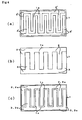
- a back-contact-type solar cell A of the present invention is constituted as follows. As shown in Fig. 1 to Fig. 4 , on a back surface 1a of a p - -type (or n - -type) semiconductor substrate 1, linear p + -type diffusion layers 2 and linear n + -type diffusion layers 3 are formed simultaneously in a state that the layers are alternately arranged close to each other. Both p + -type diffusion layers 2 and the n + -type diffusion layers 3 are separated from each other by removing a back surface 1a side of the semiconductor substrate 1 on which outer end portions of the p + -type diffusion layer 2 and the n + -type diffusion layer 3 are brought into contact with each other.
- positive and negative back surface electrodes 4, 5 are respectively connected to exposed surfaces 2a of the p + -type diffusion layers 2 and exposed surfaces 3a of the n + -type diffusion layers 3 which are separated due to the above-mentioned removal thus enabling the supply of electricity from a side opposite to a light receiving surface 1d.
- the above-mentioned p + -type diffusion layer 2 and the n + -type diffusion layer 3 are formed as follows.
- a paste 2' made of boron or the like, for example, as a p + -type impurity and a paste 3' made of phosphorus or the like, for example, as an n + -type impurity are respectively applied to the back surface 1a of the semiconductor substrate 1 made of silicon single crystal or poly-crystal silicon with desired shapes using a technique such as pattern printing.
- the paste 2' of the p + -type impurity and the paste 3' of the n + -type impurity are arranged linearly substantially parallel to each other in a state that the pastes 2' and 3' are arranged close to each other.
- the p + -type impurity 2' and the n + -type impurity 3' are respectively thermally diffused into the inside of the semiconductor substrate 1 simultaneously, and a region of the p + -type diffusion layer 2 and a region of the n + -type diffusion layer 3 are alternately and simultaneously formed in a state that the p + -type impurity 2' and the n + -type impurity 3' are arranged close to each other.
- the diffusion of the p + -type impurity 2' and the diffusion of the n + -type impurity 3' into the inside of the semiconductor substrate 1 are performed isotropically and the diffusion of the p + -type impurity 2' and the n + -type impurity 3' into a substrate portion 1c also grows due to autodoping and hence, outer end portions of the p + -type diffusion layer 2 and the n + -type diffusion layer 3 are brought into contact with each other on the back surface 1a side of the semiconductor substrate 1.
- both diffusion layers 2, 3 are separated from each other by removing the back surface 1a side of the semiconductor substrate 1 on which the outer end portions of the above-mentioned p + -type diffusion layer 2 and n + -type diffusion layer 3 are brought into contact with each other.
- a whole outer layer portion 1b of a predetermined depth from the back surface 1a of the semiconductor substrate 1 is chemically removed by an etchant or the like, or is removed mechanically by cutting using a cutting machine and hence, the respective p + -type diffusion layer 2 and n + -type diffusion layer 3 are separated from each other thus exposing a substrate portion 1c of the semiconductor substrate 1 made of silicon between the layers.
- the positive and negative back surface electrodes 4, 5 which are formed linearly in the same manner as the exposed surfaces 2a, 3a are respectively connected.
- the above-mentioned paste 2' of the p + -type impurity and the paste 3' of the n + -type impurity are printed in a comb-teeth shape by patterning.
- the region of the p + -type diffusion layer 2' and the region of n + -type diffusion layer 3' are simultaneously formed in a comb-teeth shape, and the back surface electrodes 4, 5 which are also formed in the comb-teeth shape as the p + -type diffusion layer 2 and the n + -type diffusion layer 3 are formed on the p + -type diffusion layer 2 and the n + -type diffusion layer 3 and engage with the p + -type diffusion layer 2 and n + -type diffusion layer 3 in a comb-teeth manner.
- a p + -type light receiving side diffusion layer 6 is formed when the semiconductor substrate 1 is of a p - -type, while an n + -type light receiving side diffusion layer 6 is formed when the semiconductor substrate 1 is of an n - -type.
- an anti-reflection film 7 may be formed when necessary.
- the paste 2' of the p-type impurity and the paste 3' of the n-type impurity are applied in substantially parallel to each other or in a comb-teeth shape as shown in the drawing using a technique such as pattern printing in a state that the pastes 2', 3' are linearly and alternately arranged close to each other.
- an n-type or p-type impurity paste 6' for forming the light receiving side diffusion layer 6 is applied.
- the diffusion of the p-type impurity 2' and the diffusion of the n-type impurity 3' into the inside of the semiconductor substrate 1 are performed isotropically and the diffusion of the p + -type impurity 2' and the diffusion of the n + -type impurity 3' into the substrate portion 1c also grow due to autodoping and hence, the outer end portions of the p + -type diffusion layer 2 and the n + -type diffusion layer 3 are brought into contact with each other on the back surface 1a side of the semiconductor substrate 1.
- the whole outer layer portion 1b of a predetermined depth from the back surface 1a of the semiconductor substrate 1 is chemically removed by etching or is mechanically removed by cutting using a cutting machine or the like.
- the p + -type diffusion layer 2 and the n + -type diffusion layer 3 are separated from each other thus exposing the substrate portion 1c of the semiconductor substrate 1 made of silicon therebetween.
- the above-mentioned p + -type diffusion layer 2 and the n + -type diffusion layer 3 are separately arranged in a state that the layers are arranged close to each other and hence, a distance through which electrons and positive holes generated by the incidence of light move to the p + -type diffusion layer 2 and the n + -type diffusion layer 3 is remarkably shortened thus enhancing the photoelectric conversion efficiency.
- the p + -type diffusion layer 2 and the n + -type diffusion layer 3 are formed simultaneously and hence, it is possible to obtain an advantage that both diffusion layers 2, 3 can be easily manufactured within a short time.
- the whole outer layer portion 1b of a predetermined depth from the back surface 1a of the semiconductor substrate 1 on which the outer end portions of the p + -type diffusion layer 2 and the n + -type diffusion layer 3 are brought into contact with each other is removed thus exposing the substrate portion 1c between both diffusion layers 2, 3, the p + -type diffusion layer 2 and the n + -type diffusion layer 3 are finely arranged in a state that the layers are arranged close to each other with the substrate portion 1c sandwiched therebetween and hence, it is possible to obtain an advantage that the p + -type diffusion layer 2 and the n + -type diffusion layer 3 can be easily separated from each other without the detection of a contact position between the p + -type diffusion layer 2 and the n + -type diffusion layer 3.
- both p + -type diffusion layer 2 and the n + -type diffusion layer 3 are separated from each other by removing the back surface 1a side of the semiconductor substrate 1 on which outer end portions of the diffusion layers 2, 3 are brought into contact with each other, the whole outer layer portion 1b of a predetermined depth from the back surface 1a of the semiconductor substrate 1 is removed.
- the outer end portion of the p + -type diffusion layer 2 and the outer end portion of the n + -type diffusion layer 3 may be separated from each other.
- the n + -type or p + -type light-receiving-side diffusion layer 6 is formed on the light receiving surface 1d side of the semiconductor substrate 1 and, an anti-reflection film 7 is formed on a front surface side of the light receiving side diffusion layer 6.
- the structure of the light receiving surface 1d side may be formed of other conventional known structure.
Landscapes
- Photovoltaic Devices (AREA)
Claims (1)
- Verfahren zum Herstellen einer Solarzelle vom Typ mit rückseitigem Kontakt, wobei an einer rückseitigen Oberfläche (1a) eines Halbleitersubstrats (1) abwechselnd eine lineare p+-Typ-Diffusionsschicht (2) und eine lineare n+-Typ-Diffusionsschicht (3) gebildet werden und positive und negative Rückseitenelektroden (4, 5) separat mit beiden Diffusionsschichten (2, 3) verbunden werden, wobei das Herstellungsverfahren Folgendes aufweist: in einem ersten Schritt das gleichzeitige Bilden der p+-Typ-Diffusionsschicht (2) und der n+-Typ-Diffusionsschicht (3) an der rückseitigen Oberfläche (1a) des Halbleitersubstrats (1) in einem Zustand, in dem die p+-Typ-Diffusionsschicht (2) und die n+-Typ-Diffusionsschicht (3) eng aneinander angeordnet werden und miteinander in Kontakt gebracht werden,
in einem zweiten Schritt Trennen der p+-Typ- und der n+-Typ-Diffusionsschichten (2, 3) durch Entfernen einer ganzen Außenschicht (1b) mit einer vorbestimmten Tiefe von der rückseitigen Oberfläche (1a) des Halbleitersubstrats (1), in der äußere Endteile der p+-Typ-Diffusionsschicht (2) und der n+-Typ-Diffusionsschicht (3) miteinander in Kontakt sind, wodurch nach dem Entfernen ein Teil des Halbleitersubstrats (1c) zu einer Oberfläche zwischen der p+-Typ- und der n+-Typ-biffusionsschicht hin freigelegt wird, und
in einem dritten Schritt separates Verbinden positiver und negativer Rückseitenelektroden (4, 5) mit einer freigelegten Oberfläche (2a) der p+-Typ-Diffusionsschicht (2) und einer freigelegten Oberfläche (3a) der n+-Typ-Diffusionsschicht (3), die durch den zweiten Schritt getrennt werden.
Applications Claiming Priority (2)
| Application Number | Priority Date | Filing Date | Title |
|---|---|---|---|
| JP2004376603 | 2004-12-27 | ||
| PCT/JP2005/019383 WO2006075426A1 (ja) | 2004-12-27 | 2005-10-21 | 裏面接合型太陽電池及びその製造方法 |
Publications (3)
| Publication Number | Publication Date |
|---|---|
| EP1835548A1 EP1835548A1 (de) | 2007-09-19 |
| EP1835548A4 EP1835548A4 (de) | 2010-12-01 |
| EP1835548B1 true EP1835548B1 (de) | 2012-11-28 |
Family
ID=36677460
Family Applications (1)
| Application Number | Title | Priority Date | Filing Date |
|---|---|---|---|
| EP05795521A Expired - Lifetime EP1835548B1 (de) | 2004-12-27 | 2005-10-21 | Prozess zur herstellung einer back-junction-solarzelle |
Country Status (5)
| Country | Link |
|---|---|
| US (1) | US7700400B2 (de) |
| EP (1) | EP1835548B1 (de) |
| JP (1) | JP3962086B2 (de) |
| TW (1) | TW200635058A (de) |
| WO (1) | WO2006075426A1 (de) |
Cited By (1)
| Publication number | Priority date | Publication date | Assignee | Title |
|---|---|---|---|---|
| CN103594532A (zh) * | 2013-11-21 | 2014-02-19 | 苏州阿特斯阳光电力科技有限公司 | 一种n型晶体硅太阳能电池的制备方法 |
Families Citing this family (25)
| Publication number | Priority date | Publication date | Assignee | Title |
|---|---|---|---|---|
| US7790574B2 (en) | 2004-12-20 | 2010-09-07 | Georgia Tech Research Corporation | Boron diffusion in silicon devices |
| US7820460B2 (en) * | 2007-09-07 | 2010-10-26 | Varian Semiconductor Equipment Associates, Inc. | Patterned assembly for manufacturing a solar cell and a method thereof |
| JP5236914B2 (ja) * | 2007-09-19 | 2013-07-17 | シャープ株式会社 | 太陽電池の製造方法 |
| DE112009000788T5 (de) * | 2008-04-25 | 2011-04-21 | ULVAC, Inc., Chigasaki-shi | Herstellungsverfahren für Solarzellen, Herstellungsvorrichtung für Solarzellen sowie Solarzelle |
| KR101099480B1 (ko) * | 2009-02-13 | 2011-12-27 | 엘지전자 주식회사 | 태양전지 및 그의 제조방법과 기판 식각 방법 |
| JP2010283339A (ja) * | 2009-05-02 | 2010-12-16 | Semiconductor Energy Lab Co Ltd | 光電変換装置及びその作製方法 |
| US20110132445A1 (en) * | 2009-05-29 | 2011-06-09 | Pitera Arthur J | High-efficiency multi-junction solar cell structures |
| DE102009024598A1 (de) * | 2009-06-10 | 2011-01-05 | Institut Für Solarenergieforschung Gmbh | Solarzelle mit Kontaktstruktur mit geringen Rekombinationsverlusten sowie Herstellungsverfahren für solche Solarzellen |
| US20110041910A1 (en) * | 2009-08-18 | 2011-02-24 | Semiconductor Energy Laboratory Co., Ltd. | Photoelectric conversion device and manufacturing method thereof |
| MY166305A (en) | 2009-12-09 | 2018-06-25 | Solexel Inc | High-efficiency photovoltaic back-contact solar cell structures and manufacturing methods using thin planar semiconductor absorbers |
| KR20110071374A (ko) * | 2009-12-21 | 2011-06-29 | 현대중공업 주식회사 | 후면전계형 이종접합 태양전지 및 그 제조방법 |
| EP2601687A4 (de) | 2010-08-05 | 2018-03-07 | Solexel, Inc. | Rückseitenverstärkung und vernetzungsmittel für solarzellen |
| US8633379B2 (en) | 2010-08-17 | 2014-01-21 | Lg Electronics Inc. | Solar cell |
| CN102569495B (zh) * | 2010-12-17 | 2014-03-19 | 上海凯世通半导体有限公司 | 太阳能晶片的掺杂方法 |
| CN102569493B (zh) * | 2010-12-17 | 2014-04-30 | 上海凯世通半导体有限公司 | 太阳能晶片的掺杂方法以及掺杂晶片 |
| CN102738265A (zh) * | 2011-04-15 | 2012-10-17 | 上海凯世通半导体有限公司 | 掺杂单元、掺杂晶片、掺杂方法、太阳能电池及制作方法 |
| US20150171230A1 (en) * | 2011-08-09 | 2015-06-18 | Solexel, Inc. | Fabrication methods for back contact solar cells |
| KR101225019B1 (ko) * | 2011-08-31 | 2013-01-22 | 한화케미칼 주식회사 | 선택적 펀치 쓰루를 이용한 후면 전극 태양전지의 제조방법 |
| JP6357102B2 (ja) * | 2011-11-20 | 2018-07-11 | ソレクセル、インコーポレイテッド | スマート光電池およびモジュール |
| CN103208556A (zh) * | 2012-01-13 | 2013-07-17 | 上海凯世通半导体有限公司 | 太阳能电池的制作方法及太阳能电池 |
| TWI501292B (zh) | 2012-09-26 | 2015-09-21 | 財團法人工業技術研究院 | 形成圖案化摻雜區的方法 |
| US9379258B2 (en) * | 2012-11-05 | 2016-06-28 | Solexel, Inc. | Fabrication methods for monolithically isled back contact back junction solar cells |
| US9515217B2 (en) | 2012-11-05 | 2016-12-06 | Solexel, Inc. | Monolithically isled back contact back junction solar cells |
| KR101627204B1 (ko) | 2013-11-28 | 2016-06-03 | 엘지전자 주식회사 | 태양 전지 및 이의 제조 방법 |
| US11201253B2 (en) * | 2016-11-15 | 2021-12-14 | Shin-Etsu Chemical Co., Ltd. | High photovoltaic-conversion efficiency solar cell, method for manufacturing the same, solar cell module, and photovoltaic power generation system |
Family Cites Families (14)
| Publication number | Priority date | Publication date | Assignee | Title |
|---|---|---|---|---|
| US5538564A (en) * | 1994-03-18 | 1996-07-23 | Regents Of The University Of California | Three dimensional amorphous silicon/microcrystalline silicon solar cells |
| US5641362A (en) * | 1995-11-22 | 1997-06-24 | Ebara Solar, Inc. | Structure and fabrication process for an aluminum alloy junction self-aligned back contact silicon solar cell |
| US6262359B1 (en) * | 1999-03-17 | 2001-07-17 | Ebara Solar, Inc. | Aluminum alloy back junction solar cell and a process for fabrication thereof |
| JP2002057352A (ja) * | 2000-06-02 | 2002-02-22 | Honda Motor Co Ltd | 太陽電池およびその製造方法 |
| DE10045249A1 (de) * | 2000-09-13 | 2002-04-04 | Siemens Ag | Photovoltaisches Bauelement und Verfahren zum Herstellen des Bauelements |
| JP2002164556A (ja) | 2000-11-27 | 2002-06-07 | Kyocera Corp | 裏面電極型太陽電池素子 |
| JP2003124483A (ja) | 2001-10-17 | 2003-04-25 | Toyota Motor Corp | 光起電力素子 |
| JP4074763B2 (ja) * | 2002-01-22 | 2008-04-09 | シャープ株式会社 | 太陽電池の製造方法 |
| JP2004071763A (ja) * | 2002-08-05 | 2004-03-04 | Toyota Motor Corp | 光起電力素子 |
| JP2004071828A (ja) | 2002-08-06 | 2004-03-04 | Toyota Motor Corp | 太陽電池 |
| US7339110B1 (en) * | 2003-04-10 | 2008-03-04 | Sunpower Corporation | Solar cell and method of manufacture |
| US7144751B2 (en) * | 2004-02-05 | 2006-12-05 | Advent Solar, Inc. | Back-contact solar cells and methods for fabrication |
| US7704352B2 (en) * | 2006-12-01 | 2010-04-27 | Applied Materials, Inc. | High-aspect ratio anode and apparatus for high-speed electroplating on a solar cell substrate |
| US7638438B2 (en) * | 2006-12-12 | 2009-12-29 | Palo Alto Research Center Incorporated | Solar cell fabrication using extrusion mask |
-
2005
- 2005-10-21 WO PCT/JP2005/019383 patent/WO2006075426A1/ja not_active Ceased
- 2005-10-21 JP JP2006552839A patent/JP3962086B2/ja not_active Expired - Lifetime
- 2005-10-21 US US11/722,811 patent/US7700400B2/en not_active Expired - Lifetime
- 2005-10-21 EP EP05795521A patent/EP1835548B1/de not_active Expired - Lifetime
- 2005-11-17 TW TW094140463A patent/TW200635058A/zh not_active IP Right Cessation
Cited By (2)
| Publication number | Priority date | Publication date | Assignee | Title |
|---|---|---|---|---|
| CN103594532A (zh) * | 2013-11-21 | 2014-02-19 | 苏州阿特斯阳光电力科技有限公司 | 一种n型晶体硅太阳能电池的制备方法 |
| CN103594532B (zh) * | 2013-11-21 | 2016-03-23 | 苏州阿特斯阳光电力科技有限公司 | 一种n型晶体硅太阳能电池的制备方法 |
Also Published As
| Publication number | Publication date |
|---|---|
| WO2006075426A1 (ja) | 2006-07-20 |
| TWI323040B (de) | 2010-04-01 |
| US7700400B2 (en) | 2010-04-20 |
| EP1835548A1 (de) | 2007-09-19 |
| TW200635058A (en) | 2006-10-01 |
| JP3962086B2 (ja) | 2007-08-22 |
| JPWO2006075426A1 (ja) | 2008-08-07 |
| EP1835548A4 (de) | 2010-12-01 |
| US20070264746A1 (en) | 2007-11-15 |
Similar Documents
| Publication | Publication Date | Title |
|---|---|---|
| EP1835548B1 (de) | Prozess zur herstellung einer back-junction-solarzelle | |
| US7029943B2 (en) | Photovoltaic component and module | |
| CN100401532C (zh) | 太阳能电池及其制造方法 | |
| US6143976A (en) | Solar cell with reduced shading and method of producing the same | |
| US8450602B2 (en) | Solar cell and manufacturing method thereof | |
| CN105706245B (zh) | 太阳能电池及其制造方法、太阳能电池模块 | |
| US20100276772A1 (en) | Photoelectric conversion device and method of manufacturing photoelectric conversion device | |
| JP5989259B2 (ja) | 太陽電池およびその製造方法、太陽電池モジュール | |
| CN102770968A (zh) | 背面接触太阳能电池的制造方法 | |
| US20170194520A1 (en) | Self aligned contacts for solar cells | |
| CN118335845A (zh) | 全背接触电池制造方法、全背接触电池及光伏组件 | |
| EP1870942B1 (de) | Solarzelle | |
| JP2010135562A (ja) | 光電変換素子、光電変換素子モジュールおよび光電変換素子の製造方法 | |
| JP4656996B2 (ja) | 太陽電池 | |
| WO2006075427A1 (ja) | 裏面接合型太陽電池及びその製造方法 | |
| JP2013172121A (ja) | 光電変換素子の製造方法 | |
| JP2003224289A (ja) | 太陽電池、太陽電池の接続方法、及び太陽電池モジュール | |
| KR100366348B1 (ko) | 실리콘 태양 전지의 제조 방법 | |
| JP2014239085A (ja) | 太陽電池素子およびその製造方法 | |
| JP5201659B2 (ja) | 太陽電池セル用バイパスダイオードの製造方法 | |
| JP2010263015A (ja) | 太陽電池の電極形成方法および太陽電池の製造方法 | |
| CN110121787A (zh) | 高光电变换效率太阳能电池及高光电变换效率太阳能电池的制造方法 | |
| JP2017183426A (ja) | 太陽電池セルおよび太陽電池セルの製造方法 | |
| HK1148608A (en) | Solar cell |
Legal Events
| Date | Code | Title | Description |
|---|---|---|---|
| PUAI | Public reference made under article 153(3) epc to a published international application that has entered the european phase |
Free format text: ORIGINAL CODE: 0009012 |
|
| 17P | Request for examination filed |
Effective date: 20070702 |
|
| AK | Designated contracting states |
Kind code of ref document: A1 Designated state(s): DE FR GB IT |
|
| DAX | Request for extension of the european patent (deleted) | ||
| RBV | Designated contracting states (corrected) |
Designated state(s): DE FR GB IT |
|
| A4 | Supplementary search report drawn up and despatched |
Effective date: 20101028 |
|
| 17Q | First examination report despatched |
Effective date: 20111010 |
|
| REG | Reference to a national code |
Ref country code: DE Ref legal event code: R079 Ref document number: 602005037209 Country of ref document: DE Free format text: PREVIOUS MAIN CLASS: H01L0031068000 Ipc: H01L0031180000 |
|
| RIC1 | Information provided on ipc code assigned before grant |
Ipc: H01L 31/0224 20060101ALI20120305BHEP Ipc: H01L 31/068 20120101ALI20120305BHEP Ipc: H01L 31/0352 20060101ALI20120305BHEP Ipc: H01L 31/18 20060101AFI20120305BHEP |
|
| RTI1 | Title (correction) |
Free format text: PROCESS FOR PRODUCING A BACK JUNCTION SOLAR CELL |
|
| GRAP | Despatch of communication of intention to grant a patent |
Free format text: ORIGINAL CODE: EPIDOSNIGR1 |
|
| GRAS | Grant fee paid |
Free format text: ORIGINAL CODE: EPIDOSNIGR3 |
|
| GRAP | Despatch of communication of intention to grant a patent |
Free format text: ORIGINAL CODE: EPIDOSNIGR1 |
|
| GRAA | (expected) grant |
Free format text: ORIGINAL CODE: 0009210 |
|
| AK | Designated contracting states |
Kind code of ref document: B1 Designated state(s): DE FR GB IT |
|
| REG | Reference to a national code |
Ref country code: GB Ref legal event code: FG4D |
|
| REG | Reference to a national code |
Ref country code: DE Ref legal event code: R096 Ref document number: 602005037209 Country of ref document: DE Effective date: 20130124 |
|
| PLBE | No opposition filed within time limit |
Free format text: ORIGINAL CODE: 0009261 |
|
| STAA | Information on the status of an ep patent application or granted ep patent |
Free format text: STATUS: NO OPPOSITION FILED WITHIN TIME LIMIT |
|
| 26N | No opposition filed |
Effective date: 20130829 |
|
| REG | Reference to a national code |
Ref country code: DE Ref legal event code: R097 Ref document number: 602005037209 Country of ref document: DE Effective date: 20130829 |
|
| REG | Reference to a national code |
Ref country code: FR Ref legal event code: PLFP Year of fee payment: 12 |
|
| REG | Reference to a national code |
Ref country code: FR Ref legal event code: PLFP Year of fee payment: 13 |
|
| REG | Reference to a national code |
Ref country code: FR Ref legal event code: PLFP Year of fee payment: 14 |
|
| PGFP | Annual fee paid to national office [announced via postgrant information from national office to epo] |
Ref country code: GB Payment date: 20220901 Year of fee payment: 18 |
|
| GBPC | Gb: european patent ceased through non-payment of renewal fee |
Effective date: 20231021 |
|
| PG25 | Lapsed in a contracting state [announced via postgrant information from national office to epo] |
Ref country code: GB Free format text: LAPSE BECAUSE OF NON-PAYMENT OF DUE FEES Effective date: 20231021 |
|
| PG25 | Lapsed in a contracting state [announced via postgrant information from national office to epo] |
Ref country code: GB Free format text: LAPSE BECAUSE OF NON-PAYMENT OF DUE FEES Effective date: 20231021 |
|
| PGFP | Annual fee paid to national office [announced via postgrant information from national office to epo] |
Ref country code: FR Payment date: 20240909 Year of fee payment: 20 |
|
| PGFP | Annual fee paid to national office [announced via postgrant information from national office to epo] |
Ref country code: IT Payment date: 20240910 Year of fee payment: 20 |
|
| REG | Reference to a national code |
Ref country code: DE Ref legal event code: R079 Ref document number: 602005037209 Country of ref document: DE Free format text: PREVIOUS MAIN CLASS: H01L0031180000 Ipc: H10F0071000000 |
|
| PGFP | Annual fee paid to national office [announced via postgrant information from national office to epo] |
Ref country code: DE Payment date: 20240828 Year of fee payment: 20 |
|
| REG | Reference to a national code |
Ref country code: DE Ref legal event code: R071 Ref document number: 602005037209 Country of ref document: DE |