EP1836731B1 - Transistor a film mince organique - Google Patents
Transistor a film mince organique Download PDFInfo
- Publication number
- EP1836731B1 EP1836731B1 EP06769080.0A EP06769080A EP1836731B1 EP 1836731 B1 EP1836731 B1 EP 1836731B1 EP 06769080 A EP06769080 A EP 06769080A EP 1836731 B1 EP1836731 B1 EP 1836731B1
- Authority
- EP
- European Patent Office
- Prior art keywords
- organic
- group
- layer
- formula
- compound
- Prior art date
- Legal status (The legal status is an assumption and is not a legal conclusion. Google has not performed a legal analysis and makes no representation as to the accuracy of the status listed.)
- Ceased
Links
- 0 CC(C)(C)CC(C)(C(C)(C)C)C(*Cc(cc1)ccc1C([C@](C1C2C3=CC=CC2=C2N)[C@]2N=C([*-])N*)=CC=C1c(nc1*)c3nc1C#N)=O Chemical compound CC(C)(C)CC(C)(C(C)(C)C)C(*Cc(cc1)ccc1C([C@](C1C2C3=CC=CC2=C2N)[C@]2N=C([*-])N*)=CC=C1c(nc1*)c3nc1C#N)=O 0.000 description 6
- SMLOAHWQSYUUCX-GIMYNKIXSA-N C/C(/C#N)=C(/C#N)\N=C(/C(/N=C(\CC(C12)C=CC=C1C=C1)/C3=C2C1=CCC3)=C)\NC Chemical compound C/C(/C#N)=C(/C#N)\N=C(/C(/N=C(\CC(C12)C=CC=C1C=C1)/C3=C2C1=CCC3)=C)\NC SMLOAHWQSYUUCX-GIMYNKIXSA-N 0.000 description 1
- DVYYWHZFKBUJTK-LWOQYNTDSA-N CC1([C@@H](CN)C1)C#N Chemical compound CC1([C@@H](CN)C1)C#N DVYYWHZFKBUJTK-LWOQYNTDSA-N 0.000 description 1
- WQXDOOYFUJNRGH-UHFFFAOYSA-N CN(C1c2ccc3)c4nc(C#N)c(C#N)nc4N=C1C1=C4c2c3C=CC4CC=C1 Chemical compound CN(C1c2ccc3)c4nc(C#N)c(C#N)nc4N=C1C1=C4c2c3C=CC4CC=C1 WQXDOOYFUJNRGH-UHFFFAOYSA-N 0.000 description 1
- DTLQYQNZEXNQNN-UHFFFAOYSA-N N#Cc(c(C#N)c1)cc2c1nc(c1c3c4c5cccc4ccc3ccc1)c5n2 Chemical compound N#Cc(c(C#N)c1)cc2c1nc(c1c3c4c5cccc4ccc3ccc1)c5n2 DTLQYQNZEXNQNN-UHFFFAOYSA-N 0.000 description 1
Images


Classifications
-
- B—PERFORMING OPERATIONS; TRANSPORTING
- B82—NANOTECHNOLOGY
- B82Y—SPECIFIC USES OR APPLICATIONS OF NANOSTRUCTURES; MEASUREMENT OR ANALYSIS OF NANOSTRUCTURES; MANUFACTURE OR TREATMENT OF NANOSTRUCTURES
- B82Y10/00—Nanotechnology for information processing, storage or transmission, e.g. quantum computing or single electron logic
-
- B—PERFORMING OPERATIONS; TRANSPORTING
- B82—NANOTECHNOLOGY
- B82Y—SPECIFIC USES OR APPLICATIONS OF NANOSTRUCTURES; MEASUREMENT OR ANALYSIS OF NANOSTRUCTURES; MANUFACTURE OR TREATMENT OF NANOSTRUCTURES
- B82Y30/00—Nanotechnology for materials or surface science, e.g. nanocomposites
-
- C—CHEMISTRY; METALLURGY
- C08—ORGANIC MACROMOLECULAR COMPOUNDS; THEIR PREPARATION OR CHEMICAL WORKING-UP; COMPOSITIONS BASED THEREON
- C08G—MACROMOLECULAR COMPOUNDS OBTAINED OTHERWISE THAN BY REACTIONS ONLY INVOLVING UNSATURATED CARBON-TO-CARBON BONDS
- C08G61/00—Macromolecular compounds obtained by reactions forming a carbon-to-carbon link in the main chain of the macromolecule
- C08G61/02—Macromolecular compounds containing only carbon atoms in the main chain of the macromolecule, e.g. polyxylylenes
- C08G61/04—Macromolecular compounds containing only carbon atoms in the main chain of the macromolecule, e.g. polyxylylenes only aliphatic carbon atoms
-
- C—CHEMISTRY; METALLURGY
- C08—ORGANIC MACROMOLECULAR COMPOUNDS; THEIR PREPARATION OR CHEMICAL WORKING-UP; COMPOSITIONS BASED THEREON
- C08G—MACROMOLECULAR COMPOUNDS OBTAINED OTHERWISE THAN BY REACTIONS ONLY INVOLVING UNSATURATED CARBON-TO-CARBON BONDS
- C08G61/00—Macromolecular compounds obtained by reactions forming a carbon-to-carbon link in the main chain of the macromolecule
- C08G61/12—Macromolecular compounds containing atoms other than carbon in the main chain of the macromolecule
- C08G61/122—Macromolecular compounds containing atoms other than carbon in the main chain of the macromolecule derived from five- or six-membered heterocyclic compounds, other than imides
- C08G61/123—Macromolecular compounds containing atoms other than carbon in the main chain of the macromolecule derived from five- or six-membered heterocyclic compounds, other than imides derived from five-membered heterocyclic compounds
- C08G61/124—Macromolecular compounds containing atoms other than carbon in the main chain of the macromolecule derived from five- or six-membered heterocyclic compounds, other than imides derived from five-membered heterocyclic compounds with a five-membered ring containing one nitrogen atom in the ring
-
- C—CHEMISTRY; METALLURGY
- C08—ORGANIC MACROMOLECULAR COMPOUNDS; THEIR PREPARATION OR CHEMICAL WORKING-UP; COMPOSITIONS BASED THEREON
- C08G—MACROMOLECULAR COMPOUNDS OBTAINED OTHERWISE THAN BY REACTIONS ONLY INVOLVING UNSATURATED CARBON-TO-CARBON BONDS
- C08G61/00—Macromolecular compounds obtained by reactions forming a carbon-to-carbon link in the main chain of the macromolecule
- C08G61/12—Macromolecular compounds containing atoms other than carbon in the main chain of the macromolecule
- C08G61/122—Macromolecular compounds containing atoms other than carbon in the main chain of the macromolecule derived from five- or six-membered heterocyclic compounds, other than imides
- C08G61/123—Macromolecular compounds containing atoms other than carbon in the main chain of the macromolecule derived from five- or six-membered heterocyclic compounds, other than imides derived from five-membered heterocyclic compounds
- C08G61/126—Macromolecular compounds containing atoms other than carbon in the main chain of the macromolecule derived from five- or six-membered heterocyclic compounds, other than imides derived from five-membered heterocyclic compounds with a five-membered ring containing one sulfur atom in the ring
-
- C—CHEMISTRY; METALLURGY
- C09—DYES; PAINTS; POLISHES; NATURAL RESINS; ADHESIVES; COMPOSITIONS NOT OTHERWISE PROVIDED FOR; APPLICATIONS OF MATERIALS NOT OTHERWISE PROVIDED FOR
- C09K—MATERIALS FOR MISCELLANEOUS APPLICATIONS, NOT PROVIDED FOR ELSEWHERE
- C09K11/00—Luminescent materials, e.g. electroluminescent or chemiluminescent
- C09K11/06—Luminescent materials, e.g. electroluminescent or chemiluminescent containing organic luminescent materials
-
- H—ELECTRICITY
- H10—SEMICONDUCTOR DEVICES; ELECTRIC SOLID-STATE DEVICES NOT OTHERWISE PROVIDED FOR
- H10K—ORGANIC ELECTRIC SOLID-STATE DEVICES
- H10K10/00—Organic devices specially adapted for rectifying, amplifying, oscillating or switching; Organic capacitors or resistors having potential barriers
- H10K10/80—Constructional details
- H10K10/82—Electrodes
- H10K10/84—Ohmic electrodes, e.g. source or drain electrodes
-
- H—ELECTRICITY
- H10—SEMICONDUCTOR DEVICES; ELECTRIC SOLID-STATE DEVICES NOT OTHERWISE PROVIDED FOR
- H10K—ORGANIC ELECTRIC SOLID-STATE DEVICES
- H10K85/00—Organic materials used in the body or electrodes of devices covered by this subclass
- H10K85/10—Organic polymers or oligomers
- H10K85/111—Organic polymers or oligomers comprising aromatic, heteroaromatic, or aryl chains, e.g. polyaniline, polyphenylene or polyphenylene vinylene
-
- H—ELECTRICITY
- H10—SEMICONDUCTOR DEVICES; ELECTRIC SOLID-STATE DEVICES NOT OTHERWISE PROVIDED FOR
- H10K—ORGANIC ELECTRIC SOLID-STATE DEVICES
- H10K85/00—Organic materials used in the body or electrodes of devices covered by this subclass
- H10K85/10—Organic polymers or oligomers
- H10K85/111—Organic polymers or oligomers comprising aromatic, heteroaromatic, or aryl chains, e.g. polyaniline, polyphenylene or polyphenylene vinylene
- H10K85/113—Heteroaromatic compounds comprising sulfur or selene, e.g. polythiophene
-
- H—ELECTRICITY
- H10—SEMICONDUCTOR DEVICES; ELECTRIC SOLID-STATE DEVICES NOT OTHERWISE PROVIDED FOR
- H10K—ORGANIC ELECTRIC SOLID-STATE DEVICES
- H10K85/00—Organic materials used in the body or electrodes of devices covered by this subclass
- H10K85/10—Organic polymers or oligomers
- H10K85/141—Organic polymers or oligomers comprising aliphatic or olefinic chains, e.g. poly N-vinylcarbazol, PVC or PTFE
-
- H—ELECTRICITY
- H10—SEMICONDUCTOR DEVICES; ELECTRIC SOLID-STATE DEVICES NOT OTHERWISE PROVIDED FOR
- H10K—ORGANIC ELECTRIC SOLID-STATE DEVICES
- H10K85/00—Organic materials used in the body or electrodes of devices covered by this subclass
- H10K85/60—Organic compounds having low molecular weight
- H10K85/649—Aromatic compounds comprising a hetero atom
- H10K85/657—Polycyclic condensed heteroaromatic hydrocarbons
-
- H—ELECTRICITY
- H10—SEMICONDUCTOR DEVICES; ELECTRIC SOLID-STATE DEVICES NOT OTHERWISE PROVIDED FOR
- H10K—ORGANIC ELECTRIC SOLID-STATE DEVICES
- H10K85/00—Organic materials used in the body or electrodes of devices covered by this subclass
- H10K85/60—Organic compounds having low molecular weight
- H10K85/649—Aromatic compounds comprising a hetero atom
- H10K85/657—Polycyclic condensed heteroaromatic hydrocarbons
- H10K85/6572—Polycyclic condensed heteroaromatic hydrocarbons comprising only nitrogen in the heteroaromatic polycondensed ring system, e.g. phenanthroline or carbazole
-
- C—CHEMISTRY; METALLURGY
- C09—DYES; PAINTS; POLISHES; NATURAL RESINS; ADHESIVES; COMPOSITIONS NOT OTHERWISE PROVIDED FOR; APPLICATIONS OF MATERIALS NOT OTHERWISE PROVIDED FOR
- C09K—MATERIALS FOR MISCELLANEOUS APPLICATIONS, NOT PROVIDED FOR ELSEWHERE
- C09K2211/00—Chemical nature of organic luminescent or tenebrescent compounds
- C09K2211/10—Non-macromolecular compounds
- C09K2211/1003—Carbocyclic compounds
- C09K2211/1011—Condensed systems
-
- C—CHEMISTRY; METALLURGY
- C09—DYES; PAINTS; POLISHES; NATURAL RESINS; ADHESIVES; COMPOSITIONS NOT OTHERWISE PROVIDED FOR; APPLICATIONS OF MATERIALS NOT OTHERWISE PROVIDED FOR
- C09K—MATERIALS FOR MISCELLANEOUS APPLICATIONS, NOT PROVIDED FOR ELSEWHERE
- C09K2211/00—Chemical nature of organic luminescent or tenebrescent compounds
- C09K2211/10—Non-macromolecular compounds
- C09K2211/1018—Heterocyclic compounds
- C09K2211/1025—Heterocyclic compounds characterised by ligands
- C09K2211/1044—Heterocyclic compounds characterised by ligands containing two nitrogen atoms as heteroatoms
-
- H—ELECTRICITY
- H10—SEMICONDUCTOR DEVICES; ELECTRIC SOLID-STATE DEVICES NOT OTHERWISE PROVIDED FOR
- H10K—ORGANIC ELECTRIC SOLID-STATE DEVICES
- H10K10/00—Organic devices specially adapted for rectifying, amplifying, oscillating or switching; Organic capacitors or resistors having potential barriers
- H10K10/40—Organic transistors
- H10K10/46—Field-effect transistors, e.g. organic thin-film transistors [OTFT]
- H10K10/462—Insulated gate field-effect transistors [IGFETs]
- H10K10/464—Lateral top-gate IGFETs comprising only a single gate
-
- H—ELECTRICITY
- H10—SEMICONDUCTOR DEVICES; ELECTRIC SOLID-STATE DEVICES NOT OTHERWISE PROVIDED FOR
- H10K—ORGANIC ELECTRIC SOLID-STATE DEVICES
- H10K10/00—Organic devices specially adapted for rectifying, amplifying, oscillating or switching; Organic capacitors or resistors having potential barriers
- H10K10/40—Organic transistors
- H10K10/46—Field-effect transistors, e.g. organic thin-film transistors [OTFT]
- H10K10/462—Insulated gate field-effect transistors [IGFETs]
- H10K10/466—Lateral bottom-gate IGFETs comprising only a single gate
-
- H—ELECTRICITY
- H10—SEMICONDUCTOR DEVICES; ELECTRIC SOLID-STATE DEVICES NOT OTHERWISE PROVIDED FOR
- H10K—ORGANIC ELECTRIC SOLID-STATE DEVICES
- H10K85/00—Organic materials used in the body or electrodes of devices covered by this subclass
- H10K85/60—Organic compounds having low molecular weight
- H10K85/615—Polycyclic condensed aromatic hydrocarbons, e.g. anthracene
- H10K85/621—Aromatic anhydride or imide compounds, e.g. perylene tetra-carboxylic dianhydride or perylene tetracarboxylic di-imide
Definitions
- the present invention relates to an organic thin film transistor, more particularly, to an organic thin film transistor that includes an organic layer comprising an organic compound facilitating the ohmic contact between a semi-conducting layer and electrodes.
- Thin film field-effect transistors are the basic building blocks in the fields of microelectronics. These FETs have three electrodes (e.g., a source electrode, a drain electrode, and a gate electrode), an insulating layer, and a semi-conducting layer.
- the FET functions as a capacitor where the semi-conducting layer is a conducting channel between two electrodes, i.e., the source electrode and the drain electrode.
- the density of charge carriers in the channel is adjusted by a voltage applied to the gate electrode, so that the electric charge flow between the source and the drain electrodes can be controlled by the voltage applied to the gate electrode.
- Important electronic devices which can be manufactured using semi-conducting organic materials, include organic light-emitting diodes, organic solar cells, and organic transistors.
- organic light-emitting diodes include organic light-emitting diodes, organic solar cells, and organic transistors.
- the electrical contact between the semi-conducting organic materials and the electrodes is crucial to improving the performance of these devices.
- charge-carrier injection layers such as hole-injection and electron-injection layers, are interposed between semi-conducting layers and electrodes to improve the performance of organic light-emitting diodes.
- Even though the operation mode of the organic transistor is different from that of the organic light-emitting diode, electrical contact between the semi-conducting layer and the source and drain electrodes has a profound effect upon the performance of the organic transistor.
- metals having high work functions which are noble metals, are expensive and hard to process using industrial methods, thus restricting their application processes and application structures in the organic transistors.
- JP 2003-309266 discloses an organic thin film transistor comprising a gate electrode, an insulating layer, a source electrode, a drain electrode, an organic semiconductor layer and a substrate.
- the transistor is manufactured by a method comprising the steps of subjecting a region to be in contact with the organic semiconductor layer to plasma treatment prior to forming the organic semiconductor layer.
- the present inventors have studied a method that is capable of improving the electrical contact between the semi-conducting layer and the source or drain electrode in an organic thin film transistor. Further, the present inventors have studied a method that uses an inexpensive material for the source electrode or the drain electrode of the organic thin film transistor. That is, they have studied inexpensive materials which can be used even though the materials have a low work function as the materials for the source or drain electrode of the organic thin film transistor.
- An advantage of the present invention is that it provides an organic thin film transistor that includes an organic layer comprising an organic compound facilitating the ohmic contact between a semi-conducting layer and electrodes, a method of manufacturing the same, and an electronic device including the same.
- an organic thin film transistor comprises a gate electrode, an insulating layer, a source electrode, a drain electrode, an organic semi-conducting layer, and at least one organic layer comprising a compound represented by the following formula 2, the organic layer comprising the compound represented by formula 2 being located between the organic semi-conducting layer and at least one of the source electrode and the drain electrode, and being in contact with at least one of the source electrode and the drain electrode:
- Examples of the aryl group of R9 to R18 in the above formulae include, but are not limited to, a phenyl group, a naphthyl group, an anthracenyl group, a tetracenyl group, a pentacenyl group, a biphenyl group, a terphenyl group, a benzyl group, a pyrenyl group, a perylenyl group, a coronenyl group, and the like.
- Examples of the arylamine group of R9 to R18 in the above formula 2 include, but are not limited to, a diphenylamine group, a phenylnaphthylamine group, a ditolylamine group, a phenyltolylamine group, a carbazolyl group, a triphenylamine group, and the like.
- heterocyclic group of R9 to R18 in the above formula 2 examples include, but are not limited to, a pyridyl group, an acridinyl group, a thienyl group, an imidazolyl group, an oxazolyl group, a thiazolyl group, a quinolyl group, and the like.
- halogen group of R9 to R18 in the above formula 2 examples include fluorine, chlorine, bromine and iodine.
- substituents of R9 to R18 in the above formula 2 contain other substituents
- these substituent can be selected from hydrogen, an alkyl group, an alkoxy group, an alkenyl group, an aryl group, an arylamine group, a heterocyclic group, a silane group, a boron group, an aliphatic cyclic group, an amino group, a nitrile group, a nitro group, a halogen group, an amide group, an ester group and an ether group.
- x is 2 to 10,000,000
- R19 and R20 are each independently substituted or unsubstituted C 1 -C 60 alkyl, or substituted or unsubstituted C 1 -C 60 aryl.
- the organic thin film transistor is an electronic device with three terminals called a source electrode, a drain electrode, and a gate electrode. Numerous structures of the organic thin film transistors exist. Hereinbelow, the structures of the organic thin film transistor according to the present invention will be described in detail with reference to the figures. The figures and the descriptions on the figures are provided only for the illustrative purpose, and thus the scope of the present invention is not limited thereto.
- Fig. 1 shows a cross-sectional view of a reference organic thin film transistor not according to the present invention.
- the organic thin film transistor as shown in Fig. 1 is a top-contact structure of a bottom-gate, and comprises a substrate 11, a gate electrode 16 disposed on the substrate, an insulating layer 12 disposed on the gate electrode and the substrate, a semi-conducting layer 14 disposed on the insulating layer, and a source electrode 15 and a drain electrode 11 disposed on the semi-conducting layer and the insulating layer.
- the organic thin film transistor as shown in Fig. 1 has a structure comprising a monolayered organic layer.
- the organic thin film transistor of Fig. 1 can be prepared by patterning the gate electrode 16 onto the substrate 11, forming the insulating layer 12 on the substrate and the gate electrode, forming the p- and n-type semi-conducting layer 14 on the insulating layer 12, and then forming the source electrode 15 and the drain electrode 11 on the semi-conducting layer 14 and the insulating layer 12.
- Figs. 2 to 5 illustrate organic thin film transistors according to the present invention.
- the transistors have a top-contact structure of a bottom-gate, comprising a bilayered organic layer.
- the semi-conducting layer 14 constitutes one layer
- the organic layer 17 which is inserted between the semi-conducting layer 14 and at least one electrode of the source electrode and the drain electrode constitutes the other layer.
- the organic layer 17 comprises the compound of formula 2.
- the organic thin film transistor is a structure comprising a substrate 11, a gate electrode 16 disposed on the substrate, an insulating layer 12 disposed on the gate electrode and the substrate, a semi-conducting layer 14 disposed on the insulating layer, and a source electrode 15 and a drain electrode 11 disposed on the semi-conducting layer and the insulating layer, wherein the organic layer 17 comprising the compound of formula 2 is formed to be patterned and inserted between the semi-conducting layer 14 and the source electrode 15/drain electrode 11 ( Fig. 2 ), between the semi-conducting layer 14 and the source electrode 15 ( Fig. 3 ), or between the semi-conducting layer 14 and the drain electrode 11 ( Fig. 4 ), or to be in contact with the source electrode 15 and the drain electrode 11 without patterning ( Fig. 5 ).
- the current capacity in the off-state may be increased due to the conductivity of the organic layer 17, thus it being preferable that the organic layer 17 is patterned and inserted.
- increase in the current capacity in the off-state can be suppressed.
- the charge-carrier can be formed on the semi-conducting layer 14 by applying voltage to the gate electrode 16.
- the positive charge-carrier (hole) can be formed in a p-type semi-conducting layer by using negative gate voltage
- the negative charge-carrier (electron) can be formed in an n-type semi-conducting layer by using positive gate voltage.
- the density of charge-carriers in the semi-conducting layer can be modulated by gate voltage, so that the current-flow between the source electrode and the drain electrode can be controlled by the voltage applied to the gate electrode.
- Fig. 6 shows a cross-sectional view of a further reference organic thin film transistor not according to the present invention.
- the organic thin film transistor as shown in Fig. 6 has a bottom-contact structure of a bottom-gate, which comprises a substrate 11, a gate electrode 16 disposed on the substrate, an insulating layer 12 disposed on the gate electrode and the substrate, a source electrode 15 and a drain electrode 11 disposed on the insulating layer, and a semi-conducting layer 14 disposed on the insulating layer, the source electrode and the drain electrode.
- the organic thin film transistor of Fig. 6 has a structure comprising a monolayered organic layer.
- An organic thin film transistor having a bottom-contact structure of the bottom-gate can be prepared such that it comprises a bilayered organic layer according to the present invention.
- the semi-conducting layer 14 constitutes one layer
- the organic layer 17 inserted between the semi-conducting layer 14, and at least one electrode of the source electrode and the drain electrode constitutes the other layer.
- the organic layer 17 comprises the compound of formula 2.
- the organic thin film transistor has a structure comprising a substrate 11, a gate electrode 16 disposed on the substrate, an insulating layer 12 disposed on the gate electrode and the substrate, a source electrode 15 and a drain electrode 11 disposed on the insulating layer, a semi-conducting layer 14 disposed on the insulating layer, the source electrode and the drain electrode, and the organic layer 17 comprising the compound of formula 2 is formed to be patterned and inserted between the semi-conducting layer 14 and the source electrode 15/drain electrode 11 ( Fig.
- the organic thin film transistor comprises a source electrode 15 and a drain electrode 11 disposed on the substrate 13, a semi-conducting layer 14 disposed on the substrate 13, the source electrode 15 and the drain electrode 11, an insulating layer 12 disposed on the semi-conducting layer 14, and a gate electrode 16 disposed on the insulating layer 12, wherein the organic layer 17 comprising the compound of formula 2 is further inserted between the semi-conducting layer 14 and the source electrode 15/drain electrode 11, between the semi-conducting layer 14 and the source electrode 15, or between the semi-conducting layer 14 and the drain electrode 11.
- the structure in which the organic layer 17 comprising the compound of formula 2 is inserted between the semi-conducting layer 14 and the source electrode 15/drain electrode 11 is illustrated in Fig. 10 .
- the organic thin film transistor according to another embodiment of the present invention has a structure comprising a semi-conducting layer 14 disposed on the substrate 13, a source electrode 15 and a drain electrode 11 disposed on the semi-conducting layer 14, an insulating layer 12 disposed on the semi-conducting layer 14, the source electrode 15 and the drain electrode 11, and a gate electrode 16 disposed on the insulating layer 12, wherein the organic layer 17 comprising the compound of formula 2 is inserted between the semi-conducting layer 14 and the source electrode 15/drain electrode 11, between the semi-conducting layer 14 and the source electrode 15, or between the semi-conducting layer 14 and the drain electrode 11.
- the present invention further provides a process for preparing an organic thin film transistor, comprising forming a gate electrode, an insulating layer, a source electrode, a drain electrode, an organic semi-conducting layer, and an organic layer comprising a compound represented by formula 2.
- the organic layer comprising the compound of formula 2 is formed to be in contact with the source electrode, the drain electrode or both the source electrode and the drain electrode.
- the organic layer comprising the compound of formula 2 is separately formed from the semi-conducting layer, and is formed between the semi-conducting layer and at least one electrode of the source electrode and the drain electrode.
- the process for preparing an organic thin film transistor comprises the steps of forming a gate electrode on a substrate; forming an insulating layer on the gate electrode and the substrate; forming a semi-conducting layer on the insulating layer; forming an organic layer comprising the compound of formula 2 on the semi-conducting layer; and forming a source electrode and a drain electrode on the organic layer and the insulating layer.
- the process for preparing an organic thin film transistor comprises the steps of forming a gate electrode on a substrate; forming an insulating layer on the gate electrode and the substrate; forming a source electrode and a drain electrode on the insulating layer; forming an organic layer comprising the compound of formula 2 on the insulating layer, the source electrode and the drain electrode; and forming a semi-conducting layer on the organic layer.
- the process for preparing an organic thin film transistor comprises the steps of forming a source electrode and a drain electrode on a substrate; forming an organic layer comprising the compound of formula 2 on the substrate, the source electrode and the drain electrode; forming a semi-conducting layer on the organic layer; forming an insulating layer on the semi-conducting layer; and forming a gate electrode on the insulating layer.
- the process for preparing an organic thin film transistor comprises the steps of forming a semi-conducting layer on a substrate; forming an organic layer comprising the compound of formula 2 on the semi-conducting layer; forming a source electrode and a drain electrode on the organic layer; forming an insulating layer on the organic layer, the source electrode and the drain electrode; and forming a gate electrode on the insulating layer.
- Conductive materials can be used for the gate electrode 16, including, but are not limited to, carbon, aluminum, vanadium, chromium, copper, zinc, silver, gold, magnesium, calcium, sodium, potassium, titanium, indium, yttrium, lithium, gadolinium, tin, lead, similar metals, and alloys of the foregoing metals; p- or n-doped silicon; zinc oxide, indium oxide, indium tin oxide (ITO), indium zinc oxide and similar tin oxides or tin oxide indium-based complex compounds; mixtures of oxides and metals, such as ZnO:Al, SnO 2 :Sb; and conductive polymers, such as poly(3-methylthiophene), poly[3,4-(ethylene-1,2-dioxy) thiophene], polypyrrole and polyaniline.
- p- or n-doped silicon zinc oxide, indium oxide, indium tin oxide (ITO), indium zinc oxide and similar tin oxides
- Insulator materials which can be used in the insulating layer 12 include, but are not limited to, silicon oxide, silicon nitride, and a plastic insulator such as polyimide, poly(2-vinylpyridine), poly(4-vinylphenol) and polymethyl methacrylate.
- p- and n-type organic semi-conducting materials There are two types of molecules which can be used in the semi-conducting layer: p- and n-type organic semi-conducting materials. Holes are the charge-carrier in the case of p-type semi-conducting materials while electrons are the charge-carrier in the case of n-type semi-conducting materials.
- Examples of the p-type organic semi-conducting materials include, but are not limited to, pentacene, antradithiophene, benzodithiophene, thiophene oligomers, polythiophenes, mixed-subunit thiophene oligomers, oxy-functionalized thiophene oligomers ( H. E. Katz et al., Acc. Chem. Res. 34, 359 (2001 )), and the like.
- n-type organic semi-conducting materials examples include fluorinated metallophtahlocyanines ( Z. Bao, J. Am. Chem. Soc. 120, 207 (1998 )), perfluoroarene-modified polythiophene ( A. Facchetti, Angew. Chem. Int. Ed. 42, 3900 (2003 )), and the like.
- the organic layer comprises at least one compound represented by formula 2.
- the organic layer comprising at least one compound represented by formula 2 promotes the establishment of ohmic contact between the semi-conducting layer and the source electrode, the drain electrode or both the source electrode and the drain electrode. Therefore, the threshold voltage and the charge-carrier mobility in the organic thin film transistor can be improved with the organic layer comprising at least one compound represented by formula 2.
- the organic layer comprising at least one compound represented by formula 2 can be formed using a solution process such as vacuum deposition, screen-printing, ink-jet printing, micro-contact printing, spin coating, dip coating, SAM (Self-Assembled Monolayer) and the like.
- a solution process such as vacuum deposition, screen-printing, ink-jet printing, micro-contact printing, spin coating, dip coating, SAM (Self-Assembled Monolayer) and the like.
- the compound represented by formula 2 can be selectively applied to the source electrode and the drain electrode.
- the organic layer comprising at least one compound represented by formula 2 can exhibit better effects at a thickness of several tens of nm from the monomolecular layer, preferably at a thickness as small as 100 nm from the monomolecular layer.
- Conductive materials can be used for the source electrode/drain electrode, including, but not limited to, carbon, aluminum, vanadium, chromium, copper, zinc, silver, gold, magnesium, calcium, sodium, potassium, titanium, indium, yttrium, lithium, gadolinium, tin, lead, neodymium, platinum, palladium, similar metals, and alloys of the foregoing metals; p- or n-doped silicon; zinc oxide, indium oxide, indium tin oxide (ITO), indium zinc oxide and similar tin oxides or tin oxide indium-based complex compounds; mixtures of oxides and metals, such as ZnO:Al, SnO 2 :Sb; and conductive polymers, such as poly(3-methylthiophene), poly[3,4-(ethylene-1,2-dioxy) thiophene], polypyrrole and polyaniline.
- conductive polymers such as poly(3-methylthiophene), poly[3,4-(ethylene
- materials for the source/drain electrodes have a suitable work function to reduce the charge-carrier injection barrier and form an ohmic contact with the organic layer.
- the work functions of source/drain electrode materials match or are close to a highest occupied molecular orbital (HOMO) level of the p-type organic materials. Therefore, metals with a large work function are preferred for the source electrode/drain electrode, including palladium, platinum and gold.
- HOMO occupied molecular orbital
- n-type materials are used in semi-conducting layer 14, the work functions of source/drain electrode materials match or are close to a lowest unoccupied molecular orbital (LUMO) level of the n-type organic materials. Therefore, metals with a low work function are preferred for the source electrode/drain electrode, including aluminum.
- an organic thin film transistor according to the present invention showed weak dependence on the source/drain electrode materials with the organic layer comprising the compound of formula 2. It allows us to fabricate organic thin film transistors in various ways, including screen-printing, reel-to-reel process ( J. A. Rogers et al., Adv. Mater. 11, 741 (1999 )), micro-contact printing and the like. Therefore, in the present invention, there are a variety of electrode materials that can be used for the source/drain electrode without deteriorating the performance of the organic thin film transistor with the organic layer comprising the compound of formula 2.
- aluminum can be used as the source/drain electrodes in the configuration of Fig. 10 .
- aluminum can be patterned so as to easily make the array of the source electrode 15/the drain electrode 11 by using photolithography techniques and etching methods.
- silver paste which is one of screen printable conductive inks, can be patterned by a screen-printing method to form the source electrode 15/the drain electrode 11.
- the source electrode and the drain electrode materials such as aluminum, silver, gold, neodymium, palladium, platinum, and alloys of the foregoing metals can be particularly preferably used.
- the present invention further provides an electronic device comprising the organic thin film transistor according to the present invention.
- the electronic device according to the present invention is not limited, as long as it comprises the organic thin film transistor of the present invention as a component, and it can be exemplified by an E-paper, a smart card, and a display device.
- the organic thin film transistor according to the present invention facilitates the electric contact between the semi-conducting layer and the source electrode/drain electrode with on organic layer comprising an organic compound facilitating the ohmic contact between the semi-conducting layer and source electrode/drain electrode.
- materials for the source electrode or the drain electrode in the organic thin film transistor materials which are less expensive and excellent in processibility, though they have a low work function, can be used.
- the organic thin film transistor according to the present invention has excellent electric contact between the semi-conducting layer and the source electrode/drain electrode, and thus can be widely used as a component of an electric/electronic device.
- the organic thin film transistor according to the present invention can be applied to E-papers, smart cards, and possibly display devices.
- a field-effect transistor was fabricated in a top-contact structure of a bottom-gate as shown in Fig. 5 .
- An n-doped silicon wafer was used as the substrate 13 and the gate electrode 16.
- the gate dielectric or insulating layer 12 was prepared by thermally growing silicon dioxide (SiO 2 ) on the n-doped silicon.
- the thickness of the silicon dioxide (SiO 2 ) gate insulating layer was 300 nm.
- the semi-conducting layer 14 was formed on top of the silicon dioxide (SiO 2 ) gate insulating layer 12. Pentacene was used as a p-type semi-conducting material.
- Pentacene layer 14 was deposited with a rate of 0.3 ⁇ /s under the base pressure of 1 ⁇ 10 -6 Torr. The thickness of the pentacene layer is 50 nm.
- the organic layer 17 and the gold (Au) source and drain electrodes 15 and 11, respectively, were deposited on top of the pentacene film through a shadow mask as shown in Fig. 5 .
- the organic layer 17 was deposited on top of the pentacene film prior to the deposition of the Au source electrode 15 and drain electrode 11 without patterning, as shown in Fig. 5 .
- the compound represented by Formula 2-11 was used for the formation of the organic layer 17.
- the organic layer 17 was deposited with a rate of 0.5 ⁇ /s under the base pressure of 1 ⁇ 10 -6 Torr, and the thickness of the organic layer 17 was 20 nm. As shown in Fig. 9 , the channel length (L) and the width (W) of the organic FET have profound effects on the performance of the organic thin film transistor.
- the channel length and the width of the organic thin film transistor were 1 mm and 100 ⁇ m, respectively, in accordance with Examples of the present invention.
- FIG. 11 A graph illustrating the drain-source current (I DS ) versus drain-source voltage (V DS ) characteristics for several gate voltages (V G ) is shown in Fig. 11 .
- the (I DS ) 1/2 versus V G characteristics for pentacene transistors (V DS -40V) is shown in Fig. 12 .
- a device was fabricated in the same manner as described in Example 1 except for replacing gold (Au) with aluminum (Al) as the source electrode and drain electrode.
- the organic thin film transistor comprising the organic layer 17 having aluminum as the material for the source electrode and drain electrode exhibits similar performance to that having gold as the materials for the source electrode and drain electrode.
- a device was fabricated in the same manner as described in Example 2 except for depositing the organic layer 17 on top of the pentacene film through a shadow mask in the same form as for the electrode as shown in Fig. 2 .
- FIG. 13 A graph illustrating the drain-source current (I DS ) versus drain-source voltage (V DS ) characteristics for several gate voltages (V G ) is shown in Fig. 13 .
- the (I DS ) 1/2 versus V G characteristics for pentacene transistors (V DS -40V) is shown in Fig. 14 .
- the transistor of Example 2 having the organic layer 17 not patterned, and the transistor of Example 3, having the organic layer 17 patterned, exhibited similar levels of excellent field-effect mobility.
- the transistor having the organic layer 17 not patterned (Example 2) has the same level of current capacity in the off-state to that of the transistor having the organic layer 17 patterned (Example 3), indicating that even when the organic layer 17 is not patterned, the current leakage by the organic layer 17 is not large.
- a device was fabricated in the same manner as described in Example 2 except for using the compound of the formula 2-30 upon the formation of the organic layer 17.
- FIG. 15 A graph illustrating the drain-source current (I DS ) versus drain-source voltage (V DS ) characteristics for several gate voltages (V G ) is shown in Fig. 15 .
- the (I DS ) 1/2 versus V G characteristics for pentacene transistors (V DS -40V) is shown in Fig. 16 .
- a device was fabricated in the same manner as described in Example 1 except for forming no organic layer 17.
- FIG. 17 A graph illustrating the drain-source current (I DS ) versus drain-source voltage (V DS ) characteristics for several gate voltages (V G ) is shown in Fig. 17 .
- the source-drain current has a higher value for the transistor with the organic layer 17 between pentacene and the Au electrode (Example 1, Fig. 11 ) than that for the transistor without the organic layer 17 ( Fig. 17 ). It can be found that the transistor having the organic layer 17 disposed therein facilitated the ohmic contact between the semi-conducting layer and the electrodes, thus improving the performance.
- a device was fabricated in the same manner as described in Comparative Example 1 except for replacing gold (Au) with aluminum (Al) as the source electrode/drain electrode in Comparative Example 1.
- the device did not exhibit the transistor characteristics. It can be found that when using aluminum as the source electrode/the drain electrode, the device serves as a transistor only by facilitating the ohmic contact through the disposition of the organic layer 17 to be in contact with the source electrode or the drain electrode.
- a field-effect transistor was fabricated in a bottom-contact structure of a bottom-gate as shown in Fig. 7 .
- An n-doped silicon wafer was used as the substrate 13 and the gate electrode 16.
- the gate dielectric or insulating layer 12 was prepared by thermally growing silicon dioxide (SiO 2 ) on the n-doped silicon.
- the thickness of the silicon dioxide (SiO 2 ) gate insulating layer was 300 nm.
- Gold source electrode 15 and drain electrode 11 were deposited on the silicon dioxide (SiO 2 ) gate insulating layer 12 through a shadow mask as shown in Fig. 7 .
- the organic layer 17 was deposited on the substrate having the source electrode 15 and drain electrode 11 not patterned thereon.
- the compound represented by the formula 2-11 was used for the formation of the organic layer 17.
- the organic layer 17 was deposited with a rate of 0.5 ⁇ /s under the base pressure of 1 ⁇ 10 -6 Torr.
- the thickness of the organic layer 17 was 20 nm.
- the semi-conducting layer 14 was formed on the organic layer 17 using pentacene as a p-type semi-conducting material.
- the pentacene layer 14 was deposited with a rate of 0.3 ⁇ /s under the base pressure of 1 ⁇ 10 -6 Torr.
- the thickness of pentacene layer was 50 nm.
- FIG. 19 A graph illustrating the drain-source current (I DS ) versus drain-source voltage (V DS ) characteristics for several gate voltages (V G ) is shown in Fig. 19 .
- the (I DS ) 1/2 versus V G characteristics for pentacene transistors (V DS -40V) is shown in Fig. 20 .
- THF tetrahydrofuran
- FIG. 21 A graph illustrating the drain-source current (I DS ) versus drain-source voltage (V DS ) characteristics for several gate voltages (V G ) is shown in Fig. 21 .
- the (I DS ) 1/2 versus V G characteristics for pentacene transistors (V DS -40V) is shown in Fig. 22 .
- a device was fabricated in the same manner as described in Example 5 except for forming no organic layer 17.
- FIG. 23 A graph illustrating the drain-source current (I DS ) versus drain-source voltage (V DS ) characteristics for several gate voltages (V G ) is shown in Fig. 23 .
- the transistor which is even in the bottom-contact structure facilitated the ohmic contact between the semi-conducting layer and the electrodes, thus improving the performance.
Landscapes
- Chemical & Material Sciences (AREA)
- Engineering & Computer Science (AREA)
- Materials Engineering (AREA)
- Organic Chemistry (AREA)
- Physics & Mathematics (AREA)
- Nanotechnology (AREA)
- Chemical Kinetics & Catalysis (AREA)
- Medicinal Chemistry (AREA)
- Polymers & Plastics (AREA)
- Health & Medical Sciences (AREA)
- Crystallography & Structural Chemistry (AREA)
- Spectroscopy & Molecular Physics (AREA)
- General Physics & Mathematics (AREA)
- Condensed Matter Physics & Semiconductors (AREA)
- Mathematical Physics (AREA)
- Theoretical Computer Science (AREA)
- Composite Materials (AREA)
- Thin Film Transistor (AREA)
- Nitrogen Condensed Heterocyclic Rings (AREA)
- Heterocyclic Carbon Compounds Containing A Hetero Ring Having Oxygen Or Sulfur (AREA)
- Electrodes Of Semiconductors (AREA)
Claims (18)
- Transistor à couche mince organique comprenant une électrode grille, une couche isolante, une électrode source, une électrode déversoir, une couche semi-conductrice organique et au moins une couche organique comprenant un composé représenté par la formule 2 suivante, la ou les couche(s) organique(s) comprenant un composé représenté par la formule 2 étant située(s) entre la couche semi-conductrice organique et au moins une électrode parmi l'électrode source et l'électrode déversoir, et étant en contact avec au moins une électrode parmi l'électrode source et l'électrode déversoir :
 n est 0 ou 1 ;R9 à R18 sont sélectionnés chacun indépendamment parmi un hydrogène, un groupe halogène, un groupe nitrile (-CN), un groupe nitro (-NO2), un groupe sulfonyle (-SO2R), un groupe sulfoxyde (-SOR), un groupe sulfonamide (-SO2NRR'), un groupe sulfonate (-SO3R), un groupe trifluorométhyle (-CF3), un groupe ester (COOR), un groupe amide (-CONHR, -CONRR'), un groupe alcoxy en C1 à C12 linéaire ou ramifié substitué ou non substitué, un groupe alkyle en C1 à C12 linéaire ou ramifié substitué ou non substitué, un groupe hétérocyclique aromatique ou non aromatique substitué ou non substitué, un groupe aryle en C6 à C20 substitué ou non substitué, un groupe amine substitué ou non substitué (-NHR, -NRR') et -L-M, et R9 et R10, ou R11 et R12 peuvent être liés ensemble pour former un cycle aromatique ou hétérocyclique ;L est un groupe alkylène en C1 à C60 qui est non substitué ou substitué avec au moins un groupe sélectionné parmi un groupe amine (-NHR, -NRR'), un groupe amide (-NHCOR, -CONHR, -CONRR'), un groupe éther (-COR) et un groupe ester (-COOR); un groupe arylène en C6 à C60 qui est non substitué ou substitué avec au moins un groupe sélectionné parmi un groupe amine (-NHR, -NRR'), un groupe amide (-NHCOR, -CONHR, -CONRR'), un groupe éther (-COR) et un groupe ester (-COOR) ; ou un groupe hétérocyclique de 5 à 7 chaînons qui est non substitué ou substitué avec au moins un groupe sélectionné parmi un groupe amine (-NHR, -NRR'), un groupe amide (-NHCOR, -CONHR, -CONRR'), un groupe éther (-COR) et un groupe ester (-COOR) ;M est sélectionné parmi un groupe alcool (-OH), un groupe thio (-SH), un groupe phosphate (-PO3H), un groupe amine (-NHR, -NRR'), une polyoléfine substituée ou non substituée, un polyvinyle substitué ou non substitué, un polyacrylate substitué ou non substitué, un polythiophène substitué ou non substitué, un polypyrrole substitué ou non substitué, et une polyaniline substituée ou non substituée ; etR et R' sont identiques ou différents et sont chacun indépendamment un hydrogène, un groupe alkyle en C1 à C60 substitué ou non substitué, un groupe aryle en C6 à C60 substitué ou non substitué, ou un groupe hétérocyclique de 5 à 7 chaînons substitué ou non substitué.
 - Transistor à couche mince organique selon la revendication 1, dans lequel le transistor comprend en outre un substrat, l'électrode grille est disposée sur le substrat, la couche isolante est disposée sur l'électrode grille et le substrat, la couche semi-conductrice organique est disposée sur la couche isolante, la couche organique comprenant un composé de formule 2 est disposée sur la couche semi-conductrice organique, et l'électrode source et l'électrode déversoir sont disposées sur la couche organique comprenant un composé de formule 2 et la couche isolante.
- Transistor à couche mince organique selon la revendication 1, dans lequel le transistor comprend en outre un substrat, l'électrode grille est disposée sur le substrat, la couche isolante est disposée sur l'électrode grille et le substrat, l'électrode source et l'électrode déversoir sont disposées sur la couche isolante, la couche organique comprenant un composé de formule 2 est disposée sur la couche isolante, l'électrode source et l'électrode déversoir, et la couche semi-conductrice organique est disposée sur la couche organique comprenant un composé de formule 2.
- Transistor à couche mince organique selon la revendication 1, dans lequel le transistor comprend en outre un substrat, l'électrode source et l'électrode déversoir sont disposées sur le substrat, la couche organique comprenant un composé de formule 2 est disposée sur le substrat, l'électrode source et l'électrode déversoir, la couche semi-conductrice organique est disposée sur la couche organique comprenant un composé de formule 2, la couche isolante est disposée sur la couche semi-conductrice organique, et l'électrode grille est disposée sur la couche isolante.
- Transistor à couche mince organique selon la revendication 1, dans lequel le transistor comprend en outre un substrat, la couche semi-conductrice organique est disposée sur le substrat, la couche organique comprenant un composé de formule 2 est disposée sur la couche semi-conductrice organique, l'électrode source et l'électrode déversoir sont disposées sur la couche organique comprenant un composé de formule 2, la couche isolante est disposée sur la couche organique comprenant un composé de formule 2, l'électrode source et l'électrode déversoir, et l'électrode grille est disposée sur la couche isolante.
- Transistor à couche mince organique selon la revendication 1, dans lequel le composé de formule 2 est sélectionné parmi les composés 2-1 à 2-41 suivants :


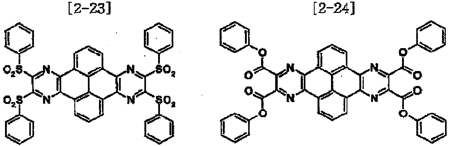


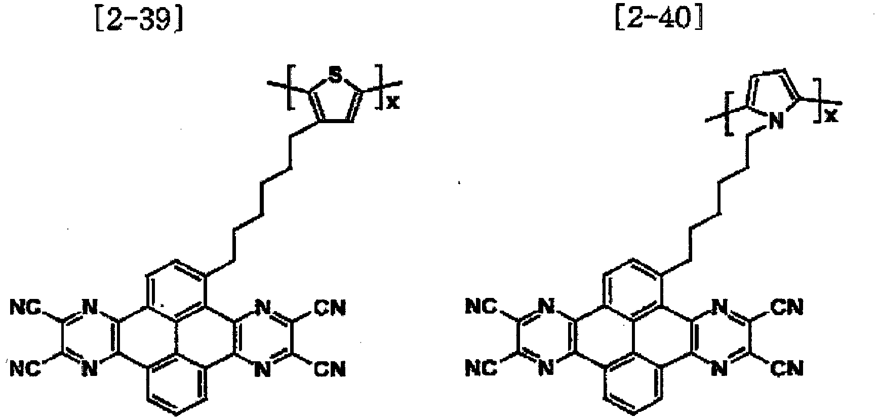

- Transistor à couche mince organique selon la revendication 1, dans lequel la couche organique comprenant un composé de formule 2 possède une épaisseur allant de l'épaisseur de la couche monomoléculaire à 100 nm.
- Transistor à couche mince organique selon la revendication 1, dans lequel l'électrode source et l'électrode déversoir sont formées à partir de matériaux sélectionnés parmi l'aluminium, l'argent, l'or, le néodyme, le palladium, le platine et les alliages des métaux susmentionnés.
- Processus de préparation d'un transistor à couche mince organique tel que défini dans la revendication 1 comprenant les étapes de formation d'une électrode grille, d'une couche isolante, d'une électrode source, d'une électrode déversoir, d'une couche semi-conductrice organique, et d'au moins une couche organique comprenant un composé représenté par la formule 2 définie dans la revendication 1, la ou les couche(s) organique(s) comprenant un composé représenté par la formule 2 étant formée(s) entre la couche semi-conductrice organique et au moins une électrode parmi l'électrode source et l'électrode déversoir afin d'être en contact avec au moins une électrode parmi l'électrode source et l'électrode déversoir.
- Processus selon la revendication 9, qui comprend les étapes de formation d'une électrode grille sur un substrat, de formation d'une couche isolante sur l'électrode grille et le substrat, de formation d'une couche semi-conductrice organique sur la couche isolante, de formation d'une couche organique comprenant un composé de formule 2 sur la couche semi-conductrice organique, et de formation d'une électrode source et d'une électrode déversoir sur la couche organique comprenant un composé de formule 2 et la couche isolante.
- Processus selon la revendication 9, qui comprend les étapes de formation d'une électrode grille sur un substrat, de formation d'une couche isolante sur l'électrode grille et le substrat, de formation d'une électrode source et d'une électrode déversoir sur la couche isolante, de formation d'une couche organique comprenant un composé de formule 2 sur la couche isolante, l'électrode source et l'électrode déversoir, et de formation d'une couche semi-conductrice organique sur la couche organique comprenant un composé de formule 2.
- Processus selon la revendication 9, qui comprend les étapes de formation d'une électrode source et d'une électrode déversoir sur un substrat, de formation d'une couche organique comprenant un composé de formule 2 sur le substrat, l'électrode source et l'électrode déversoir, de formation d'une couche semi-conductrice organique sur la couche organique comprenant un composé de formule 2, de formation d'une couche isolante sur la couche semi-conductrice organique, et de formation d'une électrode grille sur la couche isolante.
- Processus selon la revendication 9, qui comprend les étapes de formation d'une couche semi-conductrice organique sur un substrat, de formation d'une couche organique comprenant un composé de formule 2 sur la couche semi-conductrice organique, de formation d'une électrode source et d'une électrode déversoir sur la couche organique comprenant un composé de formule 2, de formation d'une couche isolante sur la couche organique comprenant un composé de formule 2, l'électrode source et l'électrode déversoir, et de formation d'une électrode grille sur la couche isolante.
- Processus selon la revendication 9, dans lequel la couche organique comprenant un composé de formule 2 possède une épaisseur allant de l'épaisseur de la couche monomoléculaire à 100 nm.
- Processus selon la revendication 9, dans lequel la couche organique comprenant un composé de formule 2 est formée par un procédé sélectionné parmi un dépôt sous vide, une sérigraphie, une impression par jet d'encre, une impression par microcontact, un revêtement par centrifugation, un revêtement par immersion et un processus d'auto-assemblage de monocouche (SAM).
- Processus selon la revendication 9, dans lequel l'électrode source et l'électrode déversoir sont formées à partir de matériaux sélectionnés parmi l'aluminium, l'argent, l'or, le néodyme, le palladium, le platine et les alliages des métaux susmentionnés.
- Dispositif électronique comprenant un transistor à couche mince organique selon la revendication 1.
- Dispositif électronique selon la revendication 17, qui est un papier électronique, une carte à puce intelligente ou un dispositif d'affichage.
Applications Claiming Priority (3)
| Application Number | Priority Date | Filing Date | Title |
|---|---|---|---|
| KR20050057717 | 2005-06-30 | ||
| KR20050107940 | 2005-11-11 | ||
| PCT/KR2006/002504 WO2007004803A2 (fr) | 2005-06-30 | 2006-06-28 | Transistor a film mince organique |
Publications (3)
| Publication Number | Publication Date |
|---|---|
| EP1836731A2 EP1836731A2 (fr) | 2007-09-26 |
| EP1836731A4 EP1836731A4 (fr) | 2012-04-25 |
| EP1836731B1 true EP1836731B1 (fr) | 2017-10-11 |
Family
ID=37604896
Family Applications (1)
| Application Number | Title | Priority Date | Filing Date |
|---|---|---|---|
| EP06769080.0A Ceased EP1836731B1 (fr) | 2005-06-30 | 2006-06-28 | Transistor a film mince organique |
Country Status (6)
| Country | Link |
|---|---|
| US (1) | US7714323B2 (fr) |
| EP (1) | EP1836731B1 (fr) |
| JP (1) | JP5031584B2 (fr) |
| KR (1) | KR100786946B1 (fr) |
| TW (1) | TWI376807B (fr) |
| WO (1) | WO2007004803A2 (fr) |
Families Citing this family (5)
| Publication number | Priority date | Publication date | Assignee | Title |
|---|---|---|---|---|
| FR2933238B1 (fr) * | 2008-06-27 | 2011-01-14 | Commissariat Energie Atomique | Nouveaux materiaux macromoleculaires semi-conducteurs organiques mesomorphes |
| US7718466B2 (en) * | 2008-07-11 | 2010-05-18 | Organicid, Inc. | Performance improvements of OFETs through use of field oxide to control ink flow |
| KR101193183B1 (ko) * | 2009-09-03 | 2012-10-19 | 삼성디스플레이 주식회사 | 헤테로고리 화합물 및 이를 이용한 유기 발광 소자 |
| KR101097314B1 (ko) * | 2009-09-03 | 2011-12-23 | 삼성모바일디스플레이주식회사 | 헤테로고리 화합물 및 이를 이용한 유기 발광 소자 |
| US8546793B2 (en) | 2010-10-26 | 2013-10-01 | Samsung Display Co., Ltd. | Organic light-emitting device |
Family Cites Families (17)
| Publication number | Priority date | Publication date | Assignee | Title |
|---|---|---|---|---|
| US5322941A (en) | 1991-01-08 | 1994-06-21 | Hoechst Aktiengesellschaft | Process for the preparation of pyrene compounds |
| JPH04283574A (ja) * | 1991-03-13 | 1992-10-08 | Mitsubishi Kasei Corp | 1,2,5−チアジアゾロピレン誘導体およびこれを用いた有機電界発光素子 |
| JP3379020B2 (ja) * | 1992-02-25 | 2003-02-17 | コニカ株式会社 | 新規なピレン系化合物及びその製造法並びに該化合物を含む電子写真感光体 |
| KR20040043116A (ko) * | 2001-04-10 | 2004-05-22 | 사르노프 코포레이션 | 유기 박막 트랜지스터를 이용한 고성능 액티브 매트릭스화소 제공방법 및 제공장치 |
| US6617609B2 (en) | 2001-11-05 | 2003-09-09 | 3M Innovative Properties Company | Organic thin film transistor with siloxane polymer interface |
| JP2003309266A (ja) * | 2002-04-17 | 2003-10-31 | Konica Minolta Holdings Inc | 有機薄膜トランジスタ素子の製造方法 |
| TWI314947B (en) * | 2002-04-24 | 2009-09-21 | Eastman Kodak Compan | Organic light emitting diode devices with improved operational stability |
| US6821811B2 (en) * | 2002-08-02 | 2004-11-23 | Semiconductor Energy Laboratory Co., Ltd. | Organic thin film transistor and method of manufacturing the same, and semiconductor device having the organic thin film transistor |
| JP4867168B2 (ja) * | 2002-09-05 | 2012-02-01 | コニカミノルタホールディングス株式会社 | 有機薄膜トランジスタの製造方法 |
| JP4429584B2 (ja) | 2002-11-07 | 2010-03-10 | 旭化成株式会社 | 縦型の電界効果トランジスタ |
| EP1434282A3 (fr) * | 2002-12-26 | 2007-06-27 | Konica Minolta Holdings, Inc. | Couche de protection pour un transistor organique à couche mince |
| JP2004335932A (ja) * | 2003-05-12 | 2004-11-25 | Konica Minolta Holdings Inc | 有機薄膜トランジスタ及びその製造方法 |
| EP1482573A3 (fr) * | 2003-05-29 | 2007-07-25 | Sony Corporation | Dispositif électroluminescent organique |
| JP2005101555A (ja) * | 2003-08-28 | 2005-04-14 | Mitsubishi Chemicals Corp | 有機電界効果トランジスタ |
| US7232619B2 (en) | 2003-10-03 | 2007-06-19 | Semiconductor Energy Laboratory Co., Ltd. | Pyrene derivative, light emitting element, and light emitting device |
| JP4795634B2 (ja) * | 2003-10-31 | 2011-10-19 | 出光興産株式会社 | 有機薄膜トランジスタ |
| JP2005260094A (ja) | 2004-03-12 | 2005-09-22 | Sharp Corp | 電子素子 |
-
2006
- 2006-06-26 KR KR1020060057582A patent/KR100786946B1/ko not_active Expired - Fee Related
- 2006-06-27 US US11/474,971 patent/US7714323B2/en active Active
- 2006-06-28 JP JP2007552073A patent/JP5031584B2/ja not_active Expired - Fee Related
- 2006-06-28 EP EP06769080.0A patent/EP1836731B1/fr not_active Ceased
- 2006-06-28 WO PCT/KR2006/002504 patent/WO2007004803A2/fr not_active Ceased
- 2006-06-30 TW TW095123837A patent/TWI376807B/zh not_active IP Right Cessation
Non-Patent Citations (1)
| Title |
|---|
| None * |
Also Published As
| Publication number | Publication date |
|---|---|
| WO2007004803A3 (fr) | 2007-04-05 |
| TW200711139A (en) | 2007-03-16 |
| EP1836731A2 (fr) | 2007-09-26 |
| KR20070003585A (ko) | 2007-01-05 |
| KR100786946B1 (ko) | 2007-12-17 |
| US20070023749A1 (en) | 2007-02-01 |
| JP2008527754A (ja) | 2008-07-24 |
| WO2007004803A2 (fr) | 2007-01-11 |
| JP5031584B2 (ja) | 2012-09-19 |
| EP1836731A4 (fr) | 2012-04-25 |
| WO2007004803A9 (fr) | 2009-07-23 |
| US7714323B2 (en) | 2010-05-11 |
| TWI376807B (en) | 2012-11-11 |
Similar Documents
| Publication | Publication Date | Title |
|---|---|---|
| CN101107716B (zh) | 有机薄膜晶体管 | |
| US6953947B2 (en) | Organic thin film transistor | |
| Yoon et al. | Organic thin-film transistors based on carbonyl-functionalized quaterthiophenes: high mobility n-channel semiconductors and ambipolar transport | |
| JP5307349B2 (ja) | 官能化ヘテロアセン類およびそれから作製された電子デバイス | |
| US7151276B2 (en) | Semiconductors containing perfluoroether acyl oligothiophene compounds | |
| KR101787121B1 (ko) | 유기 반도체 | |
| EP1672713A1 (fr) | Substance avec des groupements d'indolocarbazoles et son utilisation dans des dispositifs électroniques | |
| US8003807B2 (en) | Device containing compound having indolocarbazole moiety and divalent linkage | |
| US20080207917A1 (en) | Polymer having indolocarbazole moiety and divalent linkage | |
| CA2529245C (fr) | Procede pour former des composes comportant des groupements indolocarbazoles | |
| TW201609727A (zh) | N-氟烷基取代之二溴萘二亞胺及彼等做為半導體之用途 | |
| EP2767540A1 (fr) | Composé à base de dioxaanthanthrène, structure stratifiée et procédé de moulage associé, et dispositif électronique et son procédé de production | |
| JP2009541307A (ja) | ポリ複素環化合物、それを用いた有機電子素子およびその有機電子素子を含む電子装置 | |
| EP1836731B1 (fr) | Transistor a film mince organique | |
| CN102194998B (zh) | 有机半导体元件和有机电极 | |
| CN102844903B (zh) | 有机半导体 | |
| Gao et al. | Organic field-effect transistors based on tetrathiafulvalene derivatives | |
| JP2017141194A (ja) | 有機化合物及びその用途 | |
| US7309876B2 (en) | Organic semiconductor having polymeric and nonpolymeric constituents | |
| Facchetti | Molecular Semiconductors for Organic Field-Effect Transistors | |
| Facchetti et al. | Bisperfluorophenyl-Substituted Thiophene Oligomers. Organic Semiconductors with Complementary-Type Carrier Mobility |
Legal Events
| Date | Code | Title | Description |
|---|---|---|---|
| PUAI | Public reference made under article 153(3) epc to a published international application that has entered the european phase |
Free format text: ORIGINAL CODE: 0009012 |
|
| 17P | Request for examination filed |
Effective date: 20070720 |
|
| AK | Designated contracting states |
Kind code of ref document: A2 Designated state(s): AT BE BG CH CY CZ DE DK EE ES FI FR GB GR HU IE IS IT LI LT LU LV MC NL PL PT RO SE SI SK TR |
|
| AX | Request for extension of the european patent |
Extension state: AL BA HR MK YU |
|
| DAX | Request for extension of the european patent (deleted) | ||
| DAX | Request for extension of the european patent (deleted) | ||
| RBV | Designated contracting states (corrected) |
Designated state(s): DE GB |
|
| REG | Reference to a national code |
Ref country code: DE Ref legal event code: R079 Ref document number: 602006053839 Country of ref document: DE Free format text: PREVIOUS MAIN CLASS: H01L0029786000 Ipc: C09K0011060000 |
|
| A4 | Supplementary search report drawn up and despatched |
Effective date: 20120327 |
|
| RIC1 | Information provided on ipc code assigned before grant |
Ipc: C09K 11/06 20060101AFI20120321BHEP Ipc: C08G 61/04 20060101ALI20120321BHEP Ipc: H01L 51/00 20060101ALI20120321BHEP Ipc: H01L 29/786 20060101ALI20120321BHEP |
|
| 17Q | First examination report despatched |
Effective date: 20170208 |
|
| GRAP | Despatch of communication of intention to grant a patent |
Free format text: ORIGINAL CODE: EPIDOSNIGR1 |
|
| INTG | Intention to grant announced |
Effective date: 20170523 |
|
| GRAS | Grant fee paid |
Free format text: ORIGINAL CODE: EPIDOSNIGR3 |
|
| GRAA | (expected) grant |
Free format text: ORIGINAL CODE: 0009210 |
|
| AK | Designated contracting states |
Kind code of ref document: B1 Designated state(s): DE GB |
|
| REG | Reference to a national code |
Ref country code: GB Ref legal event code: FG4D |
|
| REG | Reference to a national code |
Ref country code: DE Ref legal event code: R096 Ref document number: 602006053839 Country of ref document: DE |
|
| REG | Reference to a national code |
Ref country code: DE Ref legal event code: R097 Ref document number: 602006053839 Country of ref document: DE |
|
| PLBE | No opposition filed within time limit |
Free format text: ORIGINAL CODE: 0009261 |
|
| STAA | Information on the status of an ep patent application or granted ep patent |
Free format text: STATUS: NO OPPOSITION FILED WITHIN TIME LIMIT |
|
| 26N | No opposition filed |
Effective date: 20180712 |
|
| GBPC | Gb: european patent ceased through non-payment of renewal fee |
Effective date: 20180628 |
|
| PG25 | Lapsed in a contracting state [announced via postgrant information from national office to epo] |
Ref country code: GB Free format text: LAPSE BECAUSE OF NON-PAYMENT OF DUE FEES Effective date: 20180628 |
|
| PGFP | Annual fee paid to national office [announced via postgrant information from national office to epo] |
Ref country code: DE Payment date: 20230522 Year of fee payment: 18 |
|
| REG | Reference to a national code |
Ref country code: DE Ref legal event code: R119 Ref document number: 602006053839 Country of ref document: DE |
|
| PG25 | Lapsed in a contracting state [announced via postgrant information from national office to epo] |
Ref country code: DE Free format text: LAPSE BECAUSE OF NON-PAYMENT OF DUE FEES Effective date: 20250101 |