EP1837670A1 - Verfahren und Vorrichtung zur Fehlerdetektion - Google Patents
Verfahren und Vorrichtung zur Fehlerdetektion Download PDFInfo
- Publication number
- EP1837670A1 EP1837670A1 EP06114800A EP06114800A EP1837670A1 EP 1837670 A1 EP1837670 A1 EP 1837670A1 EP 06114800 A EP06114800 A EP 06114800A EP 06114800 A EP06114800 A EP 06114800A EP 1837670 A1 EP1837670 A1 EP 1837670A1
- Authority
- EP
- European Patent Office
- Prior art keywords
- signal
- test signal
- test
- input
- generating
- Prior art date
- Legal status (The legal status is an assumption and is not a legal conclusion. Google has not performed a legal analysis and makes no representation as to the accuracy of the status listed.)
- Granted
Links
Images



Classifications
-
- G—PHYSICS
- G01—MEASURING; TESTING
- G01R—MEASURING ELECTRIC VARIABLES; MEASURING MAGNETIC VARIABLES
- G01R31/00—Arrangements for testing electric properties; Arrangements for locating electric faults; Arrangements for electrical testing characterised by what is being tested not provided for elsewhere
- G01R31/28—Testing of electronic circuits, e.g. by signal tracer
- G01R31/317—Testing of digital circuits
- G01R31/3181—Functional testing
- G01R31/319—Tester hardware, i.e. output processing circuits
Definitions
- This invention relates to fault detection in electrical circuits, in particular it relates to fault detection for a plurality of adjacent input circuits.
- fault tolerance is of utmost importance. Fault tolerance is the ability to continue functioning in the event of one or more failures within the system.
- Fault tolerance may be achieved by a number of different techniques, each with its specific advantages and disadvantages.
- One example of fault tolerance is known as Hardware Implemented Fault Tolerance (HIFT).
- HIFT means that the system relies on robust hardware circuits (as opposed to complex software algorithms) to perform the fault detection and redundancy management functions.
- a significant advantage HIFT has over software-implemented fault tolerance is that HIFT eliminates the overhead for communications between processors, leaving more time for controlling the process. This makes HIFT systems significantly faster and more dependable than systems using software-implemented fault tolerance.
- TMR Triple Modular Redundancy
- critical circuits are triplicated and perform identical functions simultaneously and independently.
- the data output from each of the three circuits is voted in a majority-voting circuit, before affecting the system's outputs. If one of the triplicated circuits fails, its data output is ignored. However, the system continues to output to the process the value (voltage, current level, or discrete output state) that agrees with the majority of the functional circuits.
- TMR provides continuous, predictable operation.
- HIFT and TMR provides for automatic fault recovery with no disruption to system operation and ensures minimal fault detection periods.
- Another approach to fault tolerance is the use of hot-standby modules. This approach provides a level of fault tolerance whereby the standby module maintains system operation in the event of module failure. With this approach there may be some disruption to system operation during the changeover period if the modules are not themselves fault-tolerant.
- Fault tolerant systems ideally create a Fault Containment Region (FCR) to ensure that a fault within the FCR boundary does not propagate to the remainder of the system. This enables multiple faults to co-exist on different parts of a system without affecting operation.
- FCR Fault Containment Region
- Fault tolerant systems generally employ dedicated hardware and software test and diagnostic regimes that provide very fast fault recognition and response times to provide a safer system.
- active and standby module may operate in parallel so that if an active module becomes faulty there is an automatic change over to a standby module.
- Safety control systems are generally designed to be 'fail-operational/fail-safe'. Fail operational means that when a failure occurs, the system continues to operate: it is in a fail-operational state. The system should continue to operate in this state until the failed module is replaced and the system is returned to a fully operational state.
- An example of fail safe operation occurs, for example if, in a TMR system, a failed module is not replaced before a second failure in a parallel circuit occurs, the second failure should cause the TMR system to shut down to a fail-safe state.
- Typical safety control applications include emergency and safety shutdown systems, process control, reactor control, wellhead control, turbine and compressor control, fire and gas detection and abatement, and are applicable to many industries including oil and gas production and refining, chemical production and processing, power generation, paper and textile mills and sewage treatment plants.
- a method of testing an input circuit comprising the steps of: generating a periodic test signal having a predetermined phase and a predetermined amplitude; summing the test signal and an input signal to provide a summed signal; processing the summed signal to provide an output signal; generating an extracted test signal from the output signal; comparing the extracted test signal with a reference signal representing said periodic test signal; generating an error signal in dependence upon the result of said comparing step.
- the test signal comprises a symmetrical signal and in which the output signal is sampled and averaged over a moving average period equal to an integer multiple of the period of the test signal and in which the sample period is such that the average value of the contribution from the test signal over said moving average period is equal to zero.
- test signal is a sinusoidal signal.
- the moving average period is equal to the period of the test signal. Even more preferably the period of the test signal is 4ms; the output signal is sampled every 1 ms, and an average of the previous four samples is generated every 1 ms.
- a plurality of independent input circuits are tested according to the method of any one of the preceding claims and in which a plurality of test signals are generated by a method comprising the steps of; generating a digital representation of a periodic test signal, the digital representation comprising a number of bits equal to the number of test signals to be generated; storing said digital representation in a shift register; generating a plurality of digital test signals from a plurality of taps from the shift register such that each digital test signal comprises a uniquely phased digital pattern; low pass filtering each digital test signal to generate a plurality of unique analogue test signals.
- a first test signal used to test a first input circuit is arranged to have as great a phase separation as possible from a second test signal used to test a second adjacent input circuit.
- a method of detecting in input fault in replicated input circuits in which the replicated input circuits are all arranged to receive a single input signal comprising the steps of: generating an error signal for each replicated circuit as described previously, and wherein a test signal for each replicated input circuit is arranged to have a small frequency difference with a test signal for each other replicated circuit such that in the event of one of the input circuits having an open circuit input the resulting output signal will exhibit a significant amplitude variation due to said test signals beating against one another.
- the frequency difference between the test signals for replicated input circuits is substantially equal to 0.2%.
- apparatus for testing an input circuit comprising: means for generating a periodic test signal having a predetermined phase and a predetermined amplitude; an adder for summing the test signal and an input signal to provide a summed signal; means for processing the summed signal to provide an output signal; means for generating an extracted test signal from the output signal; a comparator for comparing the extracted test signal with a reference signal representing said periodic test signal and for generating an error signal in dependence upon said comparison.
- signals 1 from an input field device are connected to the system via an input Field Termination Assembly (FTA) 2.
- An input module 3 receives, buffers and carries out any necessary conversion of the input data from the field device.
- the input data is then transmitted over a triplicated Inter-Module Bus (IMB) 5 to a TMR processor 4.
- IMB Inter-Module Bus
- Triplicated microprocessors of the TMR processor receive the input data from each channel of the IMB 5 and carry out a majority vote of the data.
- each of the three processors compares and majority votes its input data against that of the other two processors.
- the processors synchronously execute the application program, and the derived output data is transmitted back to the IMB.
- An output module 6 receives, majority votes, and carries out any necessary conversion of the output data from the TMR processor 4. The output circuits are then driven by the majority-voted command. The output signals are connected to a field device (not shown) via an output FTA 7.
- a communications interface 8 provides facilities to allow systems to be networked using peer to peer communications links, the collection of Sequence of Events (SOE) data, and connection to other systems.
- SOE Sequence of Events
- Figure 2 illustrates a sigma-delta analogue to digital (A/D) converter 10 used by the input module 3.
- the input module 3 comprises an array of 42x3 triplicated sigma-delta A/D converters 10. There is a dedicated A/D converter for each of the three input 'slices'. To maximize fault detection no buffers are inserted in the signal path.
- the sigma-delta A/D converter 10 comprises an integrator 11, a one-bit A/D converter 13 and a one-bit D/A converter 14.
- a test signal D TEST is converted by a one-bit D/A converter 15 and connected to a first input of the integrator 11 via an RC low pass filter 16.
- An input scaling resistor R IN connects an input V IN of the module to a second inverting input of the integrator 11.
- the output of the integrator 11 is converted to a digital output by the one-bit A/D converter 13.
- the one-bit D/A converter 14 feeds back an analogue version of the digital output to the inverting input via a feed back resistor R FB .
- the D TEST digital test signal is produced by an FPGA (not shown) and is unique for each of the 42x3 A/D circuits 10.
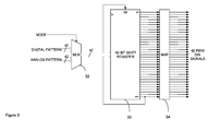
- a pattern of forty-two one's and zero's is stored in the FPGA and is circulated through a forty two bit shift register 30.
- the ratio of one's to zeros in the circulating digital pattern produces an average DC offset for an array of channels.
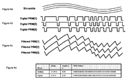
- Different patterns for example as shown in Figure 4d, are used for different input module types (eg analogue or digital) generating a different offset, allowing the centre point of the input voltage span to be tailored to suit the purpose of the module.
- the pattern to be used is selected using a multiplexer 32.
- Each tap of the shift register 30 produces a uniquely phased digital pattern as shown in Figure 4b.
- Each data stream is filtered via the D/A converter 15 and RC filter 16 shown in Figure 2, and forty two unique roughly sinusoidal signals are produced, as shown in Figure 4c.
- the system provides a new input channel result every millisecond.
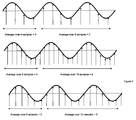
- the final result is a boxcar average of the four previous results.
- the test signal is programmed to periodically repeat at a four millisecond rate, so that it is effectively eliminated from the output signal.
- test signal repeats at a frequency equal to or an integral multiple of the frequency of a moving average (or boxcar) function and the sample period is arranged such that the average of the test signal over the moving average period is equal to zero.
- test signal could also be use so long as the sample frequency and sample period is arranged such that the resulting average of the contribution by the test signal is equal to zero.
- FIG. 7 illustrates production of an output test signal
- aserial binary sampled values are optically isolated from the output signal by an optical isolator 701.
- Isolated serial binary output samples are accumulated for 1 ms synchronously with the test signal phase by an accumulator 702.
- a 16 bit sample value is presented to a block averager 703 every ms. Four consecutive samples are averaged every ms to generate a digital output representing the analogue input.
- the test signal is extracted by sending quadrant samples Sample(0), Sample(1), Sample(2), Sample(3) to a Discrete Fourier Transformer (DFT) 704.
- DFT Discrete Fourier Transformer
- SIGNAL RE Sample 0 - Sample 2
- SIGNAL IM Sample 1 - Sample 3
- a polar co-ordinate generator 705 generates the phase and magnitude of the test signal for comparison with previously stored reference signals 706.
- a comparator 707 continuously compares the measured test signal with the reference value and generates an error condition in the event that an error is detected.
- test signals are calibrated by connecting all the inputs to a low resistance source and measuring the test signal amplitudes and phases for several seconds. These values are stored in the test signal reference memory 706 for continuous comparison during normal operating mode (see Figure 7).
- mapping function block 32 shown in Figure 3 is used to provide greatest phase separation for adjacent channels.
- the three slices are connected together and to V IN at their input resistors. If the wire between the input module and the FTA is broken, then this junction is a high impedance, and the test signal from each slice is imposed upon it. The frequencies of operation of each slice are shifted by 0.2% from each other by virtue of a programmable frequency synthesizer in the FPGA.
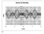
- the test signals of all the slices that are connected to the input node (and are powered up) beat against each other, ie because of the similarity of the phase a distinctive variation in amplitude of the combined signal is observed, creating a pattern that is easily recognisable. This is shown in Figure 6.
- One feature of this approach is that when standby modules are inserted in parallel to the active module, and six slices are connected to each input, the beat frequency signal components become greater because each of the six slices is running at its own unique frequency.
- the technique described here uses a continuous test signal with a unique phase and frequency for each input channel of each triplicated slice.
- the phase and amplitude of the test signals are extracted via quadrature signal processing and compared to stored reference values.
Landscapes
- General Engineering & Computer Science (AREA)
- Physics & Mathematics (AREA)
- General Physics & Mathematics (AREA)
- Engineering & Computer Science (AREA)
- Emergency Protection Circuit Devices (AREA)
- Stabilization Of Oscillater, Synchronisation, Frequency Synthesizers (AREA)
- Electronic Switches (AREA)
- Amplifiers (AREA)
- Analogue/Digital Conversion (AREA)
- Compression, Expansion, Code Conversion, And Decoders (AREA)
- Testing, Inspecting, Measuring Of Stereoscopic Televisions And Televisions (AREA)
- Synchronizing For Television (AREA)
- Hardware Redundancy (AREA)
- Testing And Monitoring For Control Systems (AREA)
- Oscillators With Electromechanical Resonators (AREA)
- Measurement Of Current Or Voltage (AREA)
- Measuring Frequencies, Analyzing Spectra (AREA)
- Transition And Organic Metals Composition Catalysts For Addition Polymerization (AREA)
- Control Of Eletrric Generators (AREA)
- Control Of Direct Current Motors (AREA)
- Tests Of Electronic Circuits (AREA)
- Monitoring And Testing Of Transmission In General (AREA)
Priority Applications (1)
| Application Number | Priority Date | Filing Date | Title |
|---|---|---|---|
| US11/689,224 US7613974B2 (en) | 2006-03-24 | 2007-03-21 | Fault detection method and apparatus |
Applications Claiming Priority (1)
| Application Number | Priority Date | Filing Date | Title |
|---|---|---|---|
| US78553706P | 2006-03-24 | 2006-03-24 |
Publications (2)
| Publication Number | Publication Date |
|---|---|
| EP1837670A1 true EP1837670A1 (de) | 2007-09-26 |
| EP1837670B1 EP1837670B1 (de) | 2018-01-03 |
Family
ID=36764483
Family Applications (7)
| Application Number | Title | Priority Date | Filing Date |
|---|---|---|---|
| EP06114800.3A Expired - Lifetime EP1837670B1 (de) | 2006-03-24 | 2006-05-31 | Verfahren und Vorrichtung zur Fehlerdetektion |
| EP06114805A Ceased EP1837971B1 (de) | 2006-03-24 | 2006-05-31 | Überlastungsschutzverfahren |
| EP06114803A Ceased EP1837991B1 (de) | 2006-03-24 | 2006-05-31 | Verfahren und Vorrichtung für Ausgangsstromsteuerung |
| EP06114806A Expired - Lifetime EP1837992B1 (de) | 2006-03-24 | 2006-05-31 | Überlastungsschutz für ein digitales Ausgangsmodul |
| EP06114804A Ceased EP1837995B1 (de) | 2006-03-24 | 2006-05-31 | Netzfrequenzsynchronisierung |
| EP06114802A Expired - Lifetime EP1837672B1 (de) | 2006-03-24 | 2006-05-31 | Verfahren und Vorrichtung zur Fehlerdetektion |
| EP06114801.1A Expired - Lifetime EP1837671B1 (de) | 2006-03-24 | 2006-05-31 | Verfahren und Vorrichtung zur Fehlerdetektion |
Family Applications After (6)
| Application Number | Title | Priority Date | Filing Date |
|---|---|---|---|
| EP06114805A Ceased EP1837971B1 (de) | 2006-03-24 | 2006-05-31 | Überlastungsschutzverfahren |
| EP06114803A Ceased EP1837991B1 (de) | 2006-03-24 | 2006-05-31 | Verfahren und Vorrichtung für Ausgangsstromsteuerung |
| EP06114806A Expired - Lifetime EP1837992B1 (de) | 2006-03-24 | 2006-05-31 | Überlastungsschutz für ein digitales Ausgangsmodul |
| EP06114804A Ceased EP1837995B1 (de) | 2006-03-24 | 2006-05-31 | Netzfrequenzsynchronisierung |
| EP06114802A Expired - Lifetime EP1837672B1 (de) | 2006-03-24 | 2006-05-31 | Verfahren und Vorrichtung zur Fehlerdetektion |
| EP06114801.1A Expired - Lifetime EP1837671B1 (de) | 2006-03-24 | 2006-05-31 | Verfahren und Vorrichtung zur Fehlerdetektion |
Country Status (3)
| Country | Link |
|---|---|
| EP (7) | EP1837670B1 (de) |
| AT (4) | ATE463066T1 (de) |
| DE (4) | DE602006013783D1 (de) |
Cited By (2)
| Publication number | Priority date | Publication date | Assignee | Title |
|---|---|---|---|---|
| CN102346206A (zh) * | 2011-09-13 | 2012-02-08 | 深圳桑菲消费通信有限公司 | 一种过热器件保护装置及方法 |
| CN105807686A (zh) * | 2016-04-05 | 2016-07-27 | 中国船舶重工集团公司第七〇二研究所 | 一种通用的隔离型开关量输入输出模块 |
Families Citing this family (8)
| Publication number | Priority date | Publication date | Assignee | Title |
|---|---|---|---|---|
| EP2096506B1 (de) | 2008-02-29 | 2013-04-24 | Rockwell Automation Limited | Verfahren und Vorrichtung zum Schutz digitaler Ausgangsschaltungen |
| CN102238752B (zh) * | 2010-04-30 | 2014-02-12 | 电信科学技术研究院 | 一种mtc设备随机接入控制方法及mtc设备 |
| CN106338983B (zh) * | 2016-09-29 | 2018-12-21 | 北京精密机电控制设备研究所 | 一种三余度数字伺服系统一度故障试验方法 |
| US10033400B1 (en) | 2017-10-18 | 2018-07-24 | Schweitzer Engineering Laboratories, Inc. | Analog-to-digital converter verification using quantization noise properties |
| US9985646B1 (en) | 2017-10-18 | 2018-05-29 | Schweitzer Engineering Laboratories, Inc. | Analog-to-digital converter verification using quantization noise properties |
| CN110132361B (zh) * | 2019-06-05 | 2021-08-06 | 重庆大学 | 一种超导限流器状态监测系统及状态监测方法 |
| EP3786649A1 (de) | 2019-08-29 | 2021-03-03 | Siemens Aktiengesellschaft | Verfahren zum überprüfen von lastkreisen in einer technischen anlage |
| CN120446075B (zh) * | 2025-07-09 | 2025-09-19 | 四川张兵兵生物科技股份有限公司 | 一种牛油中塑化剂的数字化检测装置及方法 |
Citations (7)
| Publication number | Priority date | Publication date | Assignee | Title |
|---|---|---|---|---|
| US4539683A (en) * | 1981-07-08 | 1985-09-03 | Siemens Aktiengesellschaft | Method and apparatus for checking analog-to-digital converters, digital-to-analog converters, or telecommunications transmission links which contain such converters |
| US4679028A (en) * | 1986-03-31 | 1987-07-07 | Motorola Inc. | Fault detection algorithm for successive-approximation A/D converters |
| US5552881A (en) * | 1994-03-17 | 1996-09-03 | Teradyne, Inc. | Method and apparatus for scanning a fiber optic network |
| US5594439A (en) * | 1994-08-24 | 1997-01-14 | Crystal Semiconductor Corporation | Diagnosing problems in an electrical system by monitoring changes in nonlinear characteristics |
| DE19750349A1 (de) * | 1996-11-14 | 1998-05-28 | Advantest Corp | Netzwerk-Analysator |
| US6351835B1 (en) * | 1998-07-31 | 2002-02-26 | Nec Corporation | High speed LSI spectral analysis testing apparatus and method |
| US20030063679A1 (en) * | 2001-09-06 | 2003-04-03 | Ronald Scrofano | Demodulation of multiple-carrier phase-modulated signals |
Family Cites Families (35)
| Publication number | Priority date | Publication date | Assignee | Title |
|---|---|---|---|---|
| JPS5596708A (en) * | 1979-01-19 | 1980-07-23 | Oki Electric Ind Co Ltd | Isolation amplifier circuit |
| US4535378A (en) * | 1982-11-16 | 1985-08-13 | Tokyo Shibaura Denki Kabushiki Kaisha | Overcurrent detector for an inverter |
| JPS60236073A (ja) * | 1984-05-09 | 1985-11-22 | Sumitomo Electric Ind Ltd | 送電線用フオ−ルトロケ−タ |
| SE459946B (sv) * | 1987-12-29 | 1989-08-21 | Asea Ab | Relaeskydd med selektivt fasval foer dubbelledningar |
| US5293082A (en) * | 1988-06-21 | 1994-03-08 | Western Digital Corporation | Output driver for reducing transient noise in integrated circuits |
| JP2712706B2 (ja) * | 1990-02-14 | 1998-02-16 | 国際電信電話株式会社 | 適応位相検出同期方法 |
| US5068657A (en) * | 1990-05-25 | 1991-11-26 | At&T Bell Laboratories | Method and apparatus for testing delta-sigma modulators |
| US5324989A (en) * | 1992-12-17 | 1994-06-28 | Thornton Roger D | Power controller module providing user selectable overload protection |
| US6125024A (en) * | 1993-06-03 | 2000-09-26 | Texas Instruments Incorporated | Externally programmable solid state power controller with power switch protection apparatus and method for making |
| JPH0823244A (ja) * | 1994-07-08 | 1996-01-23 | Shibaura Eng Works Co Ltd | 信号伝達装置 |
| US5909660A (en) * | 1994-10-13 | 1999-06-01 | National Instruments Corporation | Signal conditioning module for sensing multiform field voltage signals |
| US5621603A (en) * | 1995-07-26 | 1997-04-15 | United Technologies Corporation | Pulse width modulated solenoid driver controller |
| KR0158505B1 (ko) * | 1995-08-30 | 1998-12-15 | 김광호 | 부하보호기능을 갖는 전원 공급 회로 |
| DE69614659T2 (de) * | 1996-02-09 | 2004-04-08 | Co.Ri.M.Me. Consorzio Per La Ricerca Sulla Microelettronica Nel Mezzogiorno | Schaltung mit Überstromschutz für Leistungstransistoren |
| US5808415A (en) * | 1997-03-19 | 1998-09-15 | Scientific Systems Research Limited | Apparatus for sensing RF current delivered to a plasma with two inductive loops |
| US5896263A (en) * | 1997-06-27 | 1999-04-20 | Allen-Bradley Company, Llc | Output circuit having electronic overload protection activated by voltage drop across output transistor |
| US5867014A (en) * | 1997-11-20 | 1999-02-02 | Impala Linear Corporation | Current sense circuit having multiple pilot and reference transistors |
| DE19936329B4 (de) * | 1999-08-02 | 2008-03-27 | Infineon Technologies Ag | Verfahren zum A/D-Wandeln analoger Signale und entsprechende A/D-Wandleranordnung |
| US6400163B1 (en) * | 1999-09-08 | 2002-06-04 | Rolf Melcher | Circuit arrangement for monitoring an electronic switch controlling a load |
| US6320283B1 (en) * | 1999-09-10 | 2001-11-20 | Lockheed Martin Corporation | Power actuation and switching module |
| US6594129B1 (en) * | 1999-09-22 | 2003-07-15 | Yazaki Corporation | Method of cutting off circuit under overcurrent, circuit cutting-off device under overcurrent, and method of protecting semiconductor relay system |
| US6557131B1 (en) * | 1999-12-23 | 2003-04-29 | Cirrus Logic, Inc. | Apparatus and method for automated testing of integrated analog to digital converters |
| US6459599B1 (en) * | 2001-06-01 | 2002-10-01 | Otis Elevator Company | Determining phase of AC mains in PWM controlled converters without voltage sensors |
| US6633475B2 (en) * | 2001-06-22 | 2003-10-14 | Robert Bosch Corporation | High side supply shut down circuit |
| US6870328B2 (en) * | 2001-12-19 | 2005-03-22 | Toyoda Gosei Co., Ltd. | LED lamp apparatus for vehicles |
| DE10215405A1 (de) | 2002-04-08 | 2003-10-16 | Bosch Gmbh Robert | Verfahren und Vorrichtung zur Funktionsprüfung eines Analog-Digital-Wandlers sowie Analog-Digital-Wandler |
| US6768350B1 (en) * | 2002-04-10 | 2004-07-27 | Hamilton Sundstrand Corporation | Microprocessor based solid state DC power controller |
| US6657464B1 (en) * | 2002-04-25 | 2003-12-02 | Applied Micro Circuits Corporation | Method and circuit to reduce jitter generation in a PLL using a reference quadrupler, equalizer, and phase detector with control for multiple frequencies |
| GB0213882D0 (en) * | 2002-06-17 | 2002-07-31 | Univ Strathclyde | A digital system & method for testing analogue & mixed-signal circuits or systems |
| ITVA20020057A1 (it) | 2002-11-14 | 2004-05-15 | St Microelectronics Srl | Convertitore analogico digitale integrato con funzione di rilevamento di guasti esterni al dispositivo. |
| US7064946B2 (en) * | 2003-12-18 | 2006-06-20 | International Rectifier Corporation | Electronic fuse |
| FR2864418B1 (fr) * | 2003-12-19 | 2006-09-01 | Valeo Vision | Dispositif d'alimentation electrique pour diodes electroluminescentes, et projecteur lumineux comportant un tel dispositif |
| TWI233495B (en) * | 2004-02-11 | 2005-06-01 | Ind Tech Res Inst | IC with built-in self-test function and design method thereof |
| US7046180B2 (en) * | 2004-04-21 | 2006-05-16 | Rosemount Inc. | Analog-to-digital converter with range error detection |
| JP4771354B2 (ja) * | 2004-09-17 | 2011-09-14 | 株式会社小糸製作所 | 車両用灯具の点灯制御回路 |
-
2006
- 2006-05-31 EP EP06114800.3A patent/EP1837670B1/de not_active Expired - Lifetime
- 2006-05-31 EP EP06114805A patent/EP1837971B1/de not_active Ceased
- 2006-05-31 AT AT06114805T patent/ATE463066T1/de not_active IP Right Cessation
- 2006-05-31 EP EP06114803A patent/EP1837991B1/de not_active Ceased
- 2006-05-31 EP EP06114806A patent/EP1837992B1/de not_active Expired - Lifetime
- 2006-05-31 AT AT06114806T patent/ATE499747T1/de not_active IP Right Cessation
- 2006-05-31 DE DE602006013783T patent/DE602006013783D1/de not_active Expired - Lifetime
- 2006-05-31 EP EP06114804A patent/EP1837995B1/de not_active Ceased
- 2006-05-31 EP EP06114802A patent/EP1837672B1/de not_active Expired - Lifetime
- 2006-05-31 DE DE602006013269T patent/DE602006013269D1/de not_active Expired - Lifetime
- 2006-05-31 DE DE602006020243T patent/DE602006020243D1/de not_active Expired - Lifetime
- 2006-05-31 DE DE602006013268T patent/DE602006013268D1/de not_active Expired - Lifetime
- 2006-05-31 EP EP06114801.1A patent/EP1837671B1/de not_active Expired - Lifetime
- 2006-05-31 AT AT06114803T patent/ATE463077T1/de not_active IP Right Cessation
- 2006-05-31 AT AT06114804T patent/ATE465551T1/de not_active IP Right Cessation
Patent Citations (7)
| Publication number | Priority date | Publication date | Assignee | Title |
|---|---|---|---|---|
| US4539683A (en) * | 1981-07-08 | 1985-09-03 | Siemens Aktiengesellschaft | Method and apparatus for checking analog-to-digital converters, digital-to-analog converters, or telecommunications transmission links which contain such converters |
| US4679028A (en) * | 1986-03-31 | 1987-07-07 | Motorola Inc. | Fault detection algorithm for successive-approximation A/D converters |
| US5552881A (en) * | 1994-03-17 | 1996-09-03 | Teradyne, Inc. | Method and apparatus for scanning a fiber optic network |
| US5594439A (en) * | 1994-08-24 | 1997-01-14 | Crystal Semiconductor Corporation | Diagnosing problems in an electrical system by monitoring changes in nonlinear characteristics |
| DE19750349A1 (de) * | 1996-11-14 | 1998-05-28 | Advantest Corp | Netzwerk-Analysator |
| US6351835B1 (en) * | 1998-07-31 | 2002-02-26 | Nec Corporation | High speed LSI spectral analysis testing apparatus and method |
| US20030063679A1 (en) * | 2001-09-06 | 2003-04-03 | Ronald Scrofano | Demodulation of multiple-carrier phase-modulated signals |
Cited By (3)
| Publication number | Priority date | Publication date | Assignee | Title |
|---|---|---|---|---|
| CN102346206A (zh) * | 2011-09-13 | 2012-02-08 | 深圳桑菲消费通信有限公司 | 一种过热器件保护装置及方法 |
| CN105807686A (zh) * | 2016-04-05 | 2016-07-27 | 中国船舶重工集团公司第七〇二研究所 | 一种通用的隔离型开关量输入输出模块 |
| CN105807686B (zh) * | 2016-04-05 | 2018-08-10 | 中国船舶重工集团公司第七一二研究所 | 一种通用的隔离型开关量输入输出模块 |
Also Published As
| Publication number | Publication date |
|---|---|
| ATE463066T1 (de) | 2010-04-15 |
| ATE499747T1 (de) | 2011-03-15 |
| EP1837672A1 (de) | 2007-09-26 |
| EP1837670B1 (de) | 2018-01-03 |
| DE602006013269D1 (de) | 2010-05-12 |
| EP1837971A1 (de) | 2007-09-26 |
| EP1837991B1 (de) | 2010-03-31 |
| ATE463077T1 (de) | 2010-04-15 |
| DE602006013268D1 (de) | 2010-05-12 |
| EP1837671A1 (de) | 2007-09-26 |
| EP1837672B1 (de) | 2013-01-16 |
| EP1837671B1 (de) | 2017-07-12 |
| EP1837995A1 (de) | 2007-09-26 |
| ATE465551T1 (de) | 2010-05-15 |
| DE602006013783D1 (de) | 2010-06-02 |
| EP1837991A1 (de) | 2007-09-26 |
| EP1837992A1 (de) | 2007-09-26 |
| EP1837971B1 (de) | 2010-03-31 |
| EP1837992B1 (de) | 2011-02-23 |
| DE602006020243D1 (de) | 2011-04-07 |
| EP1837995B1 (de) | 2010-04-21 |
Similar Documents
| Publication | Publication Date | Title |
|---|---|---|
| US5144230A (en) | Method and system for testing integrated circuits by cycle stealing | |
| US7613974B2 (en) | Fault detection method and apparatus | |
| EP2085838B1 (de) | Eingabekanaldiagnose | |
| EP1837670B1 (de) | Verfahren und Vorrichtung zur Fehlerdetektion | |
| CN105911377B (zh) | 一种输入输出端口的测试方法 | |
| EP2595018B1 (de) | Verfahren und Vorrichtung zur Steuerung von analogem Ausgangsstrom | |
| US8166362B2 (en) | Fault detection method and apparatus for analog to digital converter circuits | |
| US5613064A (en) | Output network for a fault tolerant control system | |
| US7504975B2 (en) | Method and apparatus for output current control | |
| US7729098B2 (en) | Overload protection method | |
| KR101902577B1 (ko) | 부품을 포함하는 제어 시스템의 기능 검사 방법 | |
| US8965735B2 (en) | Signal processing device | |
| US7747405B2 (en) | Line frequency synchronization | |
| Zou et al. | Design and reliability analysis of emergency trip system with triple modular redundancy | |
| Kim et al. | Fault-tolerant architecture and reliability analysis for NISS-RPS | |
| EP0133004A2 (de) | Prüfung der zulässigen Wirkung einer einkanaligen Verarbeitungsanordnung | |
| Hammett | Computer-aided design of avionic diagnostics algorithms | |
| Murray et al. | Practical Design Considerations Affecting the Use of Digital Computers in High Voltage Substations | |
| JPS62104474A (ja) | 冗長形サイリスタバルブ故障診断方式 | |
| JP2004266918A (ja) | ディジタル保護継電装置 | |
| JPH0398327A (ja) | 二重化光信号受信装置 | |
| UA39279C2 (uk) | Система автоматичного контролю параметрів газотурбінного двигуна | |
| KR19980020949A (ko) | 철도의 연동시스템 제어장치 및 방법 | |
| JPH02104039A (ja) | デジタル多重部の自動回線試験・障害切分方式 | |
| JPH07244121A (ja) | 電子回路検査方法および電子回路検査装置 |
Legal Events
| Date | Code | Title | Description |
|---|---|---|---|
| PUAI | Public reference made under article 153(3) epc to a published international application that has entered the european phase |
Free format text: ORIGINAL CODE: 0009012 |
|
| AK | Designated contracting states |
Kind code of ref document: A1 Designated state(s): AT BE BG CH CY CZ DE DK EE ES FI FR GB GR HU IE IS IT LI LT LU LV MC NL PL PT RO SE SI SK TR |
|
| AX | Request for extension of the european patent |
Extension state: AL BA HR MK YU |
|
| 17P | Request for examination filed |
Effective date: 20080221 |
|
| 17Q | First examination report despatched |
Effective date: 20080326 |
|
| AKX | Designation fees paid |
Designated state(s): AT BE BG CH CY CZ DE DK EE ES FI FR GB GR HU IE IS IT LI LT LU LV MC NL PL PT RO SE SI SK TR |
|
| RAP1 | Party data changed (applicant data changed or rights of an application transferred) |
Owner name: ROCKWELL AUTOMATION LIMITED |
|
| GRAP | Despatch of communication of intention to grant a patent |
Free format text: ORIGINAL CODE: EPIDOSNIGR1 |
|
| INTG | Intention to grant announced |
Effective date: 20170710 |
|
| RIN1 | Information on inventor provided before grant (corrected) |
Inventor name: MEAGHER, THOMAS, BRUCE |
|
| GRAS | Grant fee paid |
Free format text: ORIGINAL CODE: EPIDOSNIGR3 |
|
| GRAJ | Information related to disapproval of communication of intention to grant by the applicant or resumption of examination proceedings by the epo deleted |
Free format text: ORIGINAL CODE: EPIDOSDIGR1 |
|
| GRAL | Information related to payment of fee for publishing/printing deleted |
Free format text: ORIGINAL CODE: EPIDOSDIGR3 |
|
| GRAR | Information related to intention to grant a patent recorded |
Free format text: ORIGINAL CODE: EPIDOSNIGR71 |
|
| GRAA | (expected) grant |
Free format text: ORIGINAL CODE: 0009210 |
|
| INTC | Intention to grant announced (deleted) | ||
| INTG | Intention to grant announced |
Effective date: 20171121 |
|
| AK | Designated contracting states |
Kind code of ref document: B1 Designated state(s): AT BE BG CH CY CZ DE DK EE ES FI FR GB GR HU IE IS IT LI LT LU LV MC NL PL PT RO SE SI SK TR |
|
| REG | Reference to a national code |
Ref country code: GB Ref legal event code: FG4D |
|
| REG | Reference to a national code |
Ref country code: CH Ref legal event code: EP Ref country code: AT Ref legal event code: REF Ref document number: 960786 Country of ref document: AT Kind code of ref document: T Effective date: 20180115 |
|
| REG | Reference to a national code |
Ref country code: IE Ref legal event code: FG4D |
|
| REG | Reference to a national code |
Ref country code: DE Ref legal event code: R096 Ref document number: 602006054459 Country of ref document: DE |
|
| REG | Reference to a national code |
Ref country code: NL Ref legal event code: MP Effective date: 20180103 |
|
| REG | Reference to a national code |
Ref country code: LT Ref legal event code: MG4D Ref country code: FR Ref legal event code: PLFP Year of fee payment: 13 |
|
| REG | Reference to a national code |
Ref country code: AT Ref legal event code: MK05 Ref document number: 960786 Country of ref document: AT Kind code of ref document: T Effective date: 20180103 |
|
| PG25 | Lapsed in a contracting state [announced via postgrant information from national office to epo] |
Ref country code: NL Free format text: LAPSE BECAUSE OF FAILURE TO SUBMIT A TRANSLATION OF THE DESCRIPTION OR TO PAY THE FEE WITHIN THE PRESCRIBED TIME-LIMIT Effective date: 20180103 |
|
| PG25 | Lapsed in a contracting state [announced via postgrant information from national office to epo] |
Ref country code: LT Free format text: LAPSE BECAUSE OF FAILURE TO SUBMIT A TRANSLATION OF THE DESCRIPTION OR TO PAY THE FEE WITHIN THE PRESCRIBED TIME-LIMIT Effective date: 20180103 Ref country code: ES Free format text: LAPSE BECAUSE OF FAILURE TO SUBMIT A TRANSLATION OF THE DESCRIPTION OR TO PAY THE FEE WITHIN THE PRESCRIBED TIME-LIMIT Effective date: 20180103 Ref country code: FI Free format text: LAPSE BECAUSE OF FAILURE TO SUBMIT A TRANSLATION OF THE DESCRIPTION OR TO PAY THE FEE WITHIN THE PRESCRIBED TIME-LIMIT Effective date: 20180103 Ref country code: CY Free format text: LAPSE BECAUSE OF FAILURE TO SUBMIT A TRANSLATION OF THE DESCRIPTION OR TO PAY THE FEE WITHIN THE PRESCRIBED TIME-LIMIT Effective date: 20180103 |
|
| PG25 | Lapsed in a contracting state [announced via postgrant information from national office to epo] |
Ref country code: LV Free format text: LAPSE BECAUSE OF FAILURE TO SUBMIT A TRANSLATION OF THE DESCRIPTION OR TO PAY THE FEE WITHIN THE PRESCRIBED TIME-LIMIT Effective date: 20180103 Ref country code: SE Free format text: LAPSE BECAUSE OF FAILURE TO SUBMIT A TRANSLATION OF THE DESCRIPTION OR TO PAY THE FEE WITHIN THE PRESCRIBED TIME-LIMIT Effective date: 20180103 Ref country code: AT Free format text: LAPSE BECAUSE OF FAILURE TO SUBMIT A TRANSLATION OF THE DESCRIPTION OR TO PAY THE FEE WITHIN THE PRESCRIBED TIME-LIMIT Effective date: 20180103 Ref country code: PL Free format text: LAPSE BECAUSE OF FAILURE TO SUBMIT A TRANSLATION OF THE DESCRIPTION OR TO PAY THE FEE WITHIN THE PRESCRIBED TIME-LIMIT Effective date: 20180103 Ref country code: IS Free format text: LAPSE BECAUSE OF FAILURE TO SUBMIT A TRANSLATION OF THE DESCRIPTION OR TO PAY THE FEE WITHIN THE PRESCRIBED TIME-LIMIT Effective date: 20180503 Ref country code: GR Free format text: LAPSE BECAUSE OF FAILURE TO SUBMIT A TRANSLATION OF THE DESCRIPTION OR TO PAY THE FEE WITHIN THE PRESCRIBED TIME-LIMIT Effective date: 20180404 Ref country code: BG Free format text: LAPSE BECAUSE OF FAILURE TO SUBMIT A TRANSLATION OF THE DESCRIPTION OR TO PAY THE FEE WITHIN THE PRESCRIBED TIME-LIMIT Effective date: 20180403 |
|
| REG | Reference to a national code |
Ref country code: DE Ref legal event code: R097 Ref document number: 602006054459 Country of ref document: DE |
|
| PG25 | Lapsed in a contracting state [announced via postgrant information from national office to epo] |
Ref country code: IT Free format text: LAPSE BECAUSE OF FAILURE TO SUBMIT A TRANSLATION OF THE DESCRIPTION OR TO PAY THE FEE WITHIN THE PRESCRIBED TIME-LIMIT Effective date: 20180103 Ref country code: EE Free format text: LAPSE BECAUSE OF FAILURE TO SUBMIT A TRANSLATION OF THE DESCRIPTION OR TO PAY THE FEE WITHIN THE PRESCRIBED TIME-LIMIT Effective date: 20180103 Ref country code: RO Free format text: LAPSE BECAUSE OF FAILURE TO SUBMIT A TRANSLATION OF THE DESCRIPTION OR TO PAY THE FEE WITHIN THE PRESCRIBED TIME-LIMIT Effective date: 20180103 |
|
| PLBE | No opposition filed within time limit |
Free format text: ORIGINAL CODE: 0009261 |
|
| STAA | Information on the status of an ep patent application or granted ep patent |
Free format text: STATUS: NO OPPOSITION FILED WITHIN TIME LIMIT |
|
| PG25 | Lapsed in a contracting state [announced via postgrant information from national office to epo] |
Ref country code: SK Free format text: LAPSE BECAUSE OF FAILURE TO SUBMIT A TRANSLATION OF THE DESCRIPTION OR TO PAY THE FEE WITHIN THE PRESCRIBED TIME-LIMIT Effective date: 20180103 Ref country code: CZ Free format text: LAPSE BECAUSE OF FAILURE TO SUBMIT A TRANSLATION OF THE DESCRIPTION OR TO PAY THE FEE WITHIN THE PRESCRIBED TIME-LIMIT Effective date: 20180103 Ref country code: DK Free format text: LAPSE BECAUSE OF FAILURE TO SUBMIT A TRANSLATION OF THE DESCRIPTION OR TO PAY THE FEE WITHIN THE PRESCRIBED TIME-LIMIT Effective date: 20180103 |
|
| 26N | No opposition filed |
Effective date: 20181005 |
|
| REG | Reference to a national code |
Ref country code: CH Ref legal event code: PL |
|
| REG | Reference to a national code |
Ref country code: BE Ref legal event code: MM Effective date: 20180531 |
|
| PG25 | Lapsed in a contracting state [announced via postgrant information from national office to epo] |
Ref country code: MC Free format text: LAPSE BECAUSE OF FAILURE TO SUBMIT A TRANSLATION OF THE DESCRIPTION OR TO PAY THE FEE WITHIN THE PRESCRIBED TIME-LIMIT Effective date: 20180103 |
|
| PG25 | Lapsed in a contracting state [announced via postgrant information from national office to epo] |
Ref country code: LI Free format text: LAPSE BECAUSE OF NON-PAYMENT OF DUE FEES Effective date: 20180531 Ref country code: SI Free format text: LAPSE BECAUSE OF FAILURE TO SUBMIT A TRANSLATION OF THE DESCRIPTION OR TO PAY THE FEE WITHIN THE PRESCRIBED TIME-LIMIT Effective date: 20180103 Ref country code: CH Free format text: LAPSE BECAUSE OF NON-PAYMENT OF DUE FEES Effective date: 20180531 |
|
| REG | Reference to a national code |
Ref country code: IE Ref legal event code: MM4A |
|
| PG25 | Lapsed in a contracting state [announced via postgrant information from national office to epo] |
Ref country code: LU Free format text: LAPSE BECAUSE OF NON-PAYMENT OF DUE FEES Effective date: 20180531 |
|
| PG25 | Lapsed in a contracting state [announced via postgrant information from national office to epo] |
Ref country code: IE Free format text: LAPSE BECAUSE OF NON-PAYMENT OF DUE FEES Effective date: 20180531 |
|
| PG25 | Lapsed in a contracting state [announced via postgrant information from national office to epo] |
Ref country code: BE Free format text: LAPSE BECAUSE OF NON-PAYMENT OF DUE FEES Effective date: 20180531 |
|
| PG25 | Lapsed in a contracting state [announced via postgrant information from national office to epo] |
Ref country code: TR Free format text: LAPSE BECAUSE OF FAILURE TO SUBMIT A TRANSLATION OF THE DESCRIPTION OR TO PAY THE FEE WITHIN THE PRESCRIBED TIME-LIMIT Effective date: 20180103 |
|
| PG25 | Lapsed in a contracting state [announced via postgrant information from national office to epo] |
Ref country code: HU Free format text: LAPSE BECAUSE OF FAILURE TO SUBMIT A TRANSLATION OF THE DESCRIPTION OR TO PAY THE FEE WITHIN THE PRESCRIBED TIME-LIMIT; INVALID AB INITIO Effective date: 20060531 Ref country code: PT Free format text: LAPSE BECAUSE OF FAILURE TO SUBMIT A TRANSLATION OF THE DESCRIPTION OR TO PAY THE FEE WITHIN THE PRESCRIBED TIME-LIMIT Effective date: 20180103 |
|
| PGFP | Annual fee paid to national office [announced via postgrant information from national office to epo] |
Ref country code: FR Payment date: 20230420 Year of fee payment: 18 Ref country code: DE Payment date: 20230419 Year of fee payment: 18 |
|
| PGFP | Annual fee paid to national office [announced via postgrant information from national office to epo] |
Ref country code: GB Payment date: 20230420 Year of fee payment: 18 |
|
| REG | Reference to a national code |
Ref country code: DE Ref legal event code: R119 Ref document number: 602006054459 Country of ref document: DE |
|
| GBPC | Gb: european patent ceased through non-payment of renewal fee |
Effective date: 20240531 |
|
| PG25 | Lapsed in a contracting state [announced via postgrant information from national office to epo] |
Ref country code: DE Free format text: LAPSE BECAUSE OF NON-PAYMENT OF DUE FEES Effective date: 20241203 |
|
| PG25 | Lapsed in a contracting state [announced via postgrant information from national office to epo] |
Ref country code: FR Free format text: LAPSE BECAUSE OF NON-PAYMENT OF DUE FEES Effective date: 20240531 |
|
| PG25 | Lapsed in a contracting state [announced via postgrant information from national office to epo] |
Ref country code: GB Free format text: LAPSE BECAUSE OF NON-PAYMENT OF DUE FEES Effective date: 20240531 |