EP1840538A2 - Zeilenbreiten-Messeinstellungsverfahren und Rasterelektronenmikroskop - Google Patents
Zeilenbreiten-Messeinstellungsverfahren und Rasterelektronenmikroskop Download PDFInfo
- Publication number
- EP1840538A2 EP1840538A2 EP07005712A EP07005712A EP1840538A2 EP 1840538 A2 EP1840538 A2 EP 1840538A2 EP 07005712 A EP07005712 A EP 07005712A EP 07005712 A EP07005712 A EP 07005712A EP 1840538 A2 EP1840538 A2 EP 1840538A2
- Authority
- EP
- European Patent Office
- Prior art keywords
- electron beam
- intensity distribution
- beam intensity
- scanning
- electron
- Prior art date
- Legal status (The legal status is an assumption and is not a legal conclusion. Google has not performed a legal analysis and makes no representation as to the accuracy of the status listed.)
- Withdrawn
Links
- 238000005259 measurement Methods 0.000 title claims abstract description 144
- 238000000034 method Methods 0.000 title claims abstract description 75
- 238000010894 electron beam technology Methods 0.000 claims abstract description 317
- 238000009826 distribution Methods 0.000 claims abstract description 170
- 230000003247 decreasing effect Effects 0.000 claims abstract description 5
- 230000001678 irradiating effect Effects 0.000 claims description 9
- 238000001514 detection method Methods 0.000 claims description 3
- 230000008569 process Effects 0.000 description 33
- 238000010586 diagram Methods 0.000 description 13
- 230000007704 transition Effects 0.000 description 6
- 239000004065 semiconductor Substances 0.000 description 4
- 238000012545 processing Methods 0.000 description 3
- 230000008859 change Effects 0.000 description 2
- 238000012937 correction Methods 0.000 description 2
- 239000002245 particle Substances 0.000 description 2
- 238000003892 spreading Methods 0.000 description 2
- 230000007480 spreading Effects 0.000 description 2
- 238000012935 Averaging Methods 0.000 description 1
- 238000013461 design Methods 0.000 description 1
- 238000003708 edge detection Methods 0.000 description 1
- 238000005530 etching Methods 0.000 description 1
- 238000004519 manufacturing process Methods 0.000 description 1
- 239000000463 material Substances 0.000 description 1
- 230000003287 optical effect Effects 0.000 description 1
- 238000011002 quantification Methods 0.000 description 1
- 230000002194 synthesizing effect Effects 0.000 description 1
Images


Classifications
-
- H—ELECTRICITY
- H01—ELECTRIC ELEMENTS
- H01J—ELECTRIC DISCHARGE TUBES OR DISCHARGE LAMPS
- H01J37/00—Discharge tubes with provision for introducing objects or material to be exposed to the discharge, e.g. for the purpose of examination or processing thereof
- H01J37/26—Electron or ion microscopes; Electron or ion diffraction tubes
- H01J37/28—Electron or ion microscopes; Electron or ion diffraction tubes with scanning beams
-
- G—PHYSICS
- G01—MEASURING; TESTING
- G01B—MEASURING LENGTH, THICKNESS OR SIMILAR LINEAR DIMENSIONS; MEASURING ANGLES; MEASURING AREAS; MEASURING IRREGULARITIES OF SURFACES OR CONTOURS
- G01B15/00—Measuring arrangements characterised by the use of electromagnetic waves or particle radiation, e.g. by the use of microwaves, X-rays, gamma rays or electrons
- G01B15/04—Measuring arrangements characterised by the use of electromagnetic waves or particle radiation, e.g. by the use of microwaves, X-rays, gamma rays or electrons for measuring contours or curvatures
-
- G—PHYSICS
- G01—MEASURING; TESTING
- G01N—INVESTIGATING OR ANALYSING MATERIALS BY DETERMINING THEIR CHEMICAL OR PHYSICAL PROPERTIES
- G01N23/00—Investigating or analysing materials by the use of wave or particle radiation, e.g. X-rays or neutrons, not covered by groups G01N3/00 – G01N17/00, G01N21/00 or G01N22/00
- G01N23/22—Investigating or analysing materials by the use of wave or particle radiation, e.g. X-rays or neutrons, not covered by groups G01N3/00 – G01N17/00, G01N21/00 or G01N22/00 by measuring secondary emission from the material
- G01N23/225—Investigating or analysing materials by the use of wave or particle radiation, e.g. X-rays or neutrons, not covered by groups G01N3/00 – G01N17/00, G01N21/00 or G01N22/00 by measuring secondary emission from the material using electron or ion
-
- H—ELECTRICITY
- H01—ELECTRIC ELEMENTS
- H01J—ELECTRIC DISCHARGE TUBES OR DISCHARGE LAMPS
- H01J2237/00—Discharge tubes exposing object to beam, e.g. for analysis treatment, etching, imaging
- H01J2237/245—Detection characterised by the variable being measured
- H01J2237/24507—Intensity, dose or other characteristics of particle beams or electromagnetic radiation
- H01J2237/24514—Beam diagnostics including control of the parameter or property diagnosed
- H01J2237/24535—Beam current
-
- H—ELECTRICITY
- H01—ELECTRIC ELEMENTS
- H01J—ELECTRIC DISCHARGE TUBES OR DISCHARGE LAMPS
- H01J2237/00—Discharge tubes exposing object to beam, e.g. for analysis treatment, etching, imaging
- H01J2237/245—Detection characterised by the variable being measured
- H01J2237/24571—Measurements of non-electric or non-magnetic variables
- H01J2237/24578—Spatial variables, e.g. position, distance
-
- H—ELECTRICITY
- H01—ELECTRIC ELEMENTS
- H01J—ELECTRIC DISCHARGE TUBES OR DISCHARGE LAMPS
- H01J2237/00—Discharge tubes exposing object to beam, e.g. for analysis treatment, etching, imaging
- H01J2237/248—Components associated with the control of the tube
-
- H—ELECTRICITY
- H01—ELECTRIC ELEMENTS
- H01J—ELECTRIC DISCHARGE TUBES OR DISCHARGE LAMPS
- H01J2237/00—Discharge tubes exposing object to beam, e.g. for analysis treatment, etching, imaging
- H01J2237/26—Electron or ion microscopes
- H01J2237/28—Scanning microscopes
- H01J2237/2813—Scanning microscopes characterised by the application
- H01J2237/2814—Measurement of surface topography
- H01J2237/2816—Length
-
- H—ELECTRICITY
- H01—ELECTRIC ELEMENTS
- H01J—ELECTRIC DISCHARGE TUBES OR DISCHARGE LAMPS
- H01J2237/00—Discharge tubes exposing object to beam, e.g. for analysis treatment, etching, imaging
- H01J2237/26—Electron or ion microscopes
- H01J2237/28—Scanning microscopes
- H01J2237/2813—Scanning microscopes characterised by the application
- H01J2237/2817—Pattern inspection
Definitions
- the present invention relates to a line-width measurement adjusting method applicable to line-width measurement of a pattern using a scanning electron microscope, or more specifically to a line-width measurement adjusting method and a scanning electron microscope capable of avoiding fluctuation in a measured value when changing magnification.
- a scanning electron microscope is configured to scan an electron beam scanning range by irradiating incident electrons, to acquire secondary electrons emitted from a sample by using a scintillator, to convert a quantity of electrons thus acquired into luminance, and to display a surface image of the sample on a display device.
- a line-width of a pattern is formed in the size within a design standard.
- the management of the pattern line-width is typically executed in accordance with the following procedures. Specifically, after displaying a predetermined range of a resist pattern formed on a semiconductor wafer on a display device, an electron beam is focused and irradiated on a measurement point in the displayed range to acquire a waveform of luminance distribution based on secondary electrons reflected from the measurement point. Then, a high-level width in the waveform of luminance distribution is determined as a line width. A judgment is made as to whether or not this line width falls within an acceptable error range. If the line width is within the acceptable error range, a subsequent etching process is executed. In contrast, if the line width is out of the acceptable error range, the wafer is sent back to a process for forming the resist pattern.
- the line-width measurement of the pattern is important in the manufacturing process of the semiconductor device, and various methods for accurately measuring the line width have been disclosed.
- a position where a slope of luminance corresponding to a quantity of secondary electrons becomes the maximum is defined as an edge position of the pattern.
- Japanese Patent Application Laid-open Publication No. Hei 5 (1993) - 296754 discloses an edge detection method of determining, as an edge position, a position where a secondary electron signal becomes the minimum.
- the line-width measurement of the pattern with a scanning electron microscope employs the method of determining the position where the slope of luminance becomes the maximum as the edge position or the method of determining the position where the secondary electron signal becomes the minimum as the edge position.
- the measurement results may vary as follows.
- use of the high magnification of observation causes an electron beam to travel in a short distance per unit time as compared to the case of use of the low magnification, whereby a range irradiated with the electron beam for a certain period of time is reduced.
- the detected edge position changes according to the size of the range irradiated with the electron beam, and this produces differences in the measurement result of the line width. For this reason, the measurement result of the line width is different between the case of high magnification of observation and the case of low magnification of observation.
- An object of the present invention is to provide a line-width measurement adjusting method for avoiding fluctuation in a measurement result when changing magnification of observation, a scanning direction or a measurement device, and to provide a scanning electron microscope having the line-width measurement adjusting method.
- the above-mentioned problems are solved by providing a line-width measurement adjusting method, which is used when first and second electron beam intensity distributions for measuring a line width are produced from intensity distribution images of secondary electrons obtained respectively by scanning a first irradiation distance with an electron beam at first magnification, and by scanning a second irradiation distance with an electron beam at second magnification.
- the method includes the step of adjusting second electron beam intensity distribution of the electron beam at the second magnification such that the second electron beam intensity distribution is equal to the first electron beam intensity distribution of the electron beam at the first magnification.
- the electron beam intensity distribution is expressed by an amount of electron beam per unit distance assuming that the amount of electron beam is measured for each unit distance in a scanning direction by scanning with the electron beam.
- a value of the electron beam intensity distribution may be obtained by firstly dividing the electron beam intensity distribution in half in the scanning direction, that is, into a primary electron beam intensity distribution and a secondary electron beam intensity distribution, and by then finding a difference in distance between the center of mass of the first electron beam intensity distribution and the center of mass of the second electron beam intensity distribution.
- the second electron beam intensity distribution may be adjusted by increasing or decreasing the second irradiation distance when producing the electron beam intensity distribution.
- the electron beam intensity distribution is adjusted so as to equalize the values of electron beam intensity distribution in terms of the respective amounts of travel each showing the distribution of the irradiated electron beam.
- the distances in the scanning direction of irradiation of the electron beams become almost equal even when the line-width is measured by rescaling the magnification of observation. Accordingly, it is possible to prevent different measurement results of the line width.
- the above-mentioned problems are resolved by providing a line-width measurement adjusting method using an intensity distribution image of secondary electrons obtained by scanning a first irradiation distance with an electron beam having a first beam diameter and an intensity distribution image of secondary electrons obtained by scanning a second irradiation distance with an electron beam having a second beam diameter.
- the method includes the step of adjusting second electron beam intensity distribution of the electron beam having the second beam diameter when producing electron beam intensity distribution for measuring a line width such that first electron beam intensity distribution of the electron beam having the first beam diameter becomes equal to the second electron beam intensity distribution.
- the above-mentioned problems are resolved by providing a line-width measurement adjusting method using an intensity distribution image of secondary electrons obtained by scanning a first irradiation distance with an electron beam configured to scan in a first direction and an intensity distribution image of secondary electrons obtained by scanning a second irradiation distance with an electron beam configured to scan in a second direction.
- the method includes the step of adjusting second electron beam intensity distribution of the electron beam scanning in the second direction when producing electron beam intensity distribution for measuring a line width such that first electron beam intensity distribution of the electron beam scanning in the first direction equal to the second electron beam intensity distribution.
- the distances of irradiation of the electron beams are equalized by adjusting the electron beam intensity distribution. Accordingly, it is possible to prevent different measurement results between the scanning electron microscopes.
- the distances irradiated with the electron beam are equalized by adjusting the electron beam intensity distribution depending on the scanning direction. Accordingly, it is possible to prevent different measurement results depending on the scanning direction.
- another aspect of the present invention provides a scanning electron microscope that embodies the line-width measurement adjusting method according to the above-described aspects.
- An example of the scanning electron microscope of this aspect includes an electron gun for irradiating an electron beam onto a surface of a sample, an electron detection unit for detecting electrons emitted from the sample upon irradiation of the electron beam, and a control unit for adjusting second electron beam intensity distribution of the electron beam at second magnification such that first electron beam intensity distribution of the electron beam at first magnification becomes equal to the second electron beam intensity distribution.
- a configuration of a scanning electron microscope will be described in the first place. Then, a typical method of measuring a line width of a pattern will be described. Thereafter, an adjusting method for the line-width measurement in the case of changing magnification of observation or other factors will be described. Lastly, the line-width measurement using a line-width measurement adjusting method of the present invention will be described.
- Fig. 1 is a block diagram of a scanning electron microscope according to an embodiment of the present invention.
- This scanning electron microscope 100 essentially includes an electron scanning unit 10, a signal processing unit 30, an image display unit 40, and a control unit 20 for controlling the electron scanning unit 10, the signal processing unit 30, and the image display unit 40.
- the electron scanning unit 10 includes an electron gun 1, a condenser lens 2, a deflecting coil 3, an object lens 4, a motion stage 5, and a sample holder 6.
- Charged particles 9 are emitted from the electron gun 1 and irradiated onto a sample 7 on the motion stag 5 through the condenser lens 2, the deflecting coil 3, and the object lens 4.
- a quantity of secondary electrons or reflected electrons coming out of the sample 7 upon irradiation of the charged particles 9 is detected by an electron detector 8 formed of a scintillator, for example, and the detected quantity is converted into a digital amount by an AD converter and further into a luminance signal used for display on the image display unit 40.
- control unit 20 An electron deflection amount by the deflecting coil 3 and an image scanning amount by the image display unit 40 are controlled by the control unit 20. Meanwhile, the control unit 20 stores a program for executing line-width measurement.
- the sample 7 used herein includes a foundation layer 50 formed on a semiconductor wafer, and a line pattern 51 formed on the foundation layer 50.
- This line pattern 51 is a pattern targeted for dimensional management.
- Part of the sample 7 is formed into a planar shape as shown in Fig. 2A.
- a portion surrounded by a broken line 52 indicates an observation area of the scanning electron microscope 100.
- Fig. 2B shows an example of an image display, which is achieved by detecting the quantity of electrons such as secondary electrons with the electron detector by scanning the sample with an electron beam shown in Fig. 2A, converting the detected quantity of electrons into the luminance signal, and forming the image display by synchronizing the electron beam scanning and CRT scanning.
- Fig. 2C is a view showing the quantity of electrons emitted from or reflected by the sample obtained at the time of irradiating the electron beam along the I-I line in Fig. 2A.
- the quantity of electrons such as secondary electrons emitted from the sample upon irradiation of the electron beam varies depending on a surface condition of the sample.
- the quantity of emitted electrons is low if the sample has a flat surface. If the surface of the sample is inclined, the secondary electrons emitted laterally from a lower side of a slope travel for a short distance inside the sample. Accordingly, the amount of emitted electrons is increased as compared to the case of the flat surface.
- the quantity of emitted or reflected electrons varies depending on the material on which the electron beam is irradiated.
- a signal amount converted into luminance is low in a flat surface area where no line patterns are formed.
- the signal amount is increased in an area where the line pattern is formed.
- a line width is measured by calculating such edge positions.
- the surface condition of the sample is observed by scanning the sample with the electron beam and calculating the condition by use of the quantity of electrons such as secondary electrons emitted from the surface of the sample.
- An electron microscopic image representing the surface condition varies depending on the point on the sample for which the quantity of electrons is used for calculation. For example, it is possible to express the surface condition more accurately in the case of a narrow interval between the points on the surface for acquiring the quantities of electrons such as secondary electrons as compared to the case of a wider interval.
- the point for acquiring the quantity of electrons such as secondary electrons is called as a measurement point.
- magnification of observation is high, the electron beam scans a narrower range as compared to a case where the magnification of observation is low. This is due to the fact that the electron beam scans the narrower range in the case of the high magnification of observation as compared to the case of the lower magnification of observation.
- a scanning time remains the same.
- Figs. 3A and 3B show electron beam intensity distribution obtained by electron beam scanning while setting two different values of magnification.
- the electron beam intensity distribution is expressed by an amount of electron beam per unit distance assuming that the amount of electron beam is measured for each unit distance in a scanning direction by scanning with the electron beam.
- Fig. 3A shows the electron beam intensity distribution showing the amount of electron beam per unit distance when setting the distance in the scanning direction for irradiating the electron beam equal to 5.
- Fig. 3B shows the electron beam intensity distribution showing the amount of electron beam per unit distance when setting the distance in the scanning direction for irradiating the electron beam equal to 3.
- Fig. 3A shows the example where the magnification of observation is set lower than the case in Fig. 3B, and a scanning time period is set equal between the case in Fig. 3A and the case in Fig. 3B.
- the distance in the scanning direction for irradiating the electron beam is determined by the magnification of observation and the scanning time period. Even if the scanning time period is set constant, the scanning distance is different when rescaling the magnification of observation. For this reason, the amounts of secondary electrons emitted from the sample beam are different when irradiating the electron beam for two different scanning distances. Consequently, the measurement result changes in spite of the same pattern.
- the electron beam intensity distribution in the case of scanning a predetermined distance is obtained respectively in terms of the magnification of observation as a standard and in terms of the magnification of observation different from the standard, and the electron beam intensity distribution obtained at the magnification of observation different from the standard is adjusted equal to the electron beam intensity distribution obtained at the standard magnification of observation.
- the adjustment of the electron beam intensity distribution obtained at the magnification of observation different from the standard is achieved by increasing or decreasing an irradiation distance of the electron beam from an image obtained by scanning the predetermined distance at the magnification of observation different from the standard when producing the electron beam intensity distribution. In this way, the distance in the scanning direction of the electron beam irradiation is set equal when the magnification of observation is different.
- the electron beam intensity distribution shown in Fig. 3A is defined as the standard
- the electron beam intensity distribution shown in Fig. 3B is adjusted to form the distribution equal to the electron beam intensity distribution shown in Fig. 3A.
- the scanning distance in Fig. 3B is changed such that the distance of irradiation of the electron beam in the scanning direction therein becomes an approximate value to the distance in Fig. 3A.
- a judgment as to whether or not the two types of the electron beam intensity distribution are equal is made by comparing the values representing the respective types of the electron beam intensity distribution.
- the value representing the electron beam intensity distribution is defined by dividing the electron beam intensity distribution in half along the scanning direction, calculating the center of mass for each of segments of the distribution divided in half, and finding a difference in distance between the centers of mass thus calculated.
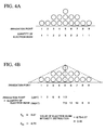
- Fig. 4A shows an example of the electron beam intensity distribution, in which the amount of electron beam of the measurement point located per unit distance is expressed in the number of unit electron beam amounts (indicated with circles).
- the electron beam intensity distribution in Fig. 4A has a spread of coordinates of the irradiation points (coordinates in the scanning direction) ranging from 1 to 9.
- the amount of electron beam at the irradiation point 3 is equal to 2, for example.
- the electron beam intensity distribution shown in Fig. 4A is divided in half into a former half distribution segment and a latter half distribution segment along the scanning direction of the electron beam as shown in Fig. 4B.
- the former half distribution segment ranges from 5 to 9 on the coordinate axis and the latter half distribution segment ranges from 1 to 5 on the coordinate axis.
- the value of the former distribution segment is calculated by defining a multiplied value of the coordinate value in the scanning direction indicating the irradiation point of the electron beam and a total value of the unit electron beam irradiated on that irradiation point as the quantity of electron beam at that irradiation point and then dividing a sum of the quantities of electron beam in the respective irradiation points in the former distribution segment by a total of the unit electron beam amounts irradiated in the former distribution segment.
- the value of the latter distribution segment is calculated by defining the multiplied value of the coordinate value in the scanning direction indicating the irradiation point of the electron beam and the total value of the unit electron beam irradiated on that irradiation point as the quantity of electron beam at that irradiation point and then dividing a sum of the quantities of electron beam in the respective irradiation points in the latter distribution segment by a total of the unit electron beam amounts irradiated in the latter distribution segment.
- X 0 is the center of mass
- X i is the irradiation point per unit distance
- P i is the quantity of electron beam irradiated on the irradiation point X i .
- the difference in distance between the center of mass of the former distribution segment and the center of mass of the latter distribution segment in the electron beam intensity distribution will also be referred to as an effective irradiation travel distance.
- the electron beam When the electron beam travels, the electron beam is irradiated in the size determined by a beam diameter. Accordingly, it is not possible to detect only the secondary electrons emitted by the electron beam irradiated on the measurement point x on the surface of the sample.
- the electron beam is also irradiated on a portion ahead of the measurement point x in the scanning direction. As a result, the secondary electrons emitted by the electron beam irradiated on the portion ahead in the scanning direction are also detected. In this way, the electron beam has a certain spread from the measurement point toward the scanning direction. For this reason, the quantity of electrons at the measurement point includes not only the quantity of electrons obtained from the measurement point but also the quantity of electrons obtained from the spread range of the electron beam.
- the electron beam is assumed to be composed of a unit electron beam having the size determined by the beam diameter, and the spread of the electron beam is assumed to be equal to a distance that the unit electron beam advances for 2 unit time periods.
- Fig. 5A shows the case of low magnification which indicates that the electron beam spreads and irradiates for 5 unit distance that is equivalent to a distance encompassing 5 pieces of unit electron beams (B1, B2, B3, B4, and B5).
- the electron beam in this spread range is equivalent to an "electron beam spreading in the scanning direction from the measurement point to a distance depending on a scanning speed". This electron beam will be hereinafter referred to as an "extended electron beam”.
- Fig. 5B shows the case of high magnification in which the extended electron beam spreads for 3 unit distance that is equivalent to a distance encompassing 3 pieces of unit electron beams (B6, B7, and B8).
- Figs. 6A and 6B are diagrams showing the electron beam intensity distribution in the case of measurement with three measurement points, i.e., at the measurement time t 1 to 3.
- Fig. 6A schematically shows the continuously traveling electron beam in the form of discrete transition of the extended electron beam.
- the second row represents the electron beam irradiated on the sample when the electron beam travels at a lapse of a certain short time from the time of the first row.
- the third row represents the electron beam irradiated on the sample when the electron beam travels at a lapse of the certain short time from the time of the second row.
- Fig. 6B shows the electron beam intensity distribution obtained by summing up the quantity of electron beam for each unit distance. As shown in the drawing, when there are three measurement points, the distance in the scanning direction of the irradiation of the electron beam covers the irradiation points having the coordinate values from 1 to 9. Moreover, the drawing shows that the quantity of electron beam is equal to 3 at the irradiation point 5.
- the electron beam intensity distribution obtained in Figs. 6A and 6B is defined as standard electron beam intensity distribution
- a process to adjust the electron beam intensity distribution obtained at the magnification of observation different from that used in Figs. 6A and 6B will be described below.
- the electron beam intensity distribution in Fig. 6B is the same as the electron beam intensity distribution in Fig. 4A and that the standard effective irradiation travel distance SEID is equal to 3.46.
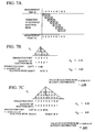
- Figs. 7A to 7C are diagrams showing transition of the extended electron beam when setting the magnification of observation applied hereto is set twice as large as the magnification of observation (defined as standard magnification) used for obtaining the standard electron beam intensity distribution.
- Fig. 7A schematically shows the continuously traveling electron beam in the form of transition of the discrete extended electron beam.
- Fig. 7A applies the magnification of observation which is twice as large as that used in Fig. 6A. Accordingly, the coverage of the measurement points (the irradiation points) at each measurement time period is narrower as compared to Fig. 6A.
- Fig. 8 is a flowchart showing a process to equalize the electron beam intensity distribution of Figs. 7A to 7C to the standard electron beam intensity distribution.
- initial setting is performed in step S1 in Fig. 8.
- the number of measurement points N is set to 1.
- the standard effective irradiation travel distance SEID is calculated in advance.
- the electron beam intensity distribution shown in Figs. 6A and 6B is defined as the standard electron beam intensity distribution and the standard effective irradiation travel distance SEID is equal to 3.46.
- the effective irradiation travel distance EID is compared with the standard effective irradiation travel distance SEID in the next step S3.
- a predetermined value ⁇ such as 0.2
- the process goes to step S5 to determine the number of measurement points equal to N and then the process is completed.
- the process goes to step S4 when the absolute value of the difference between the effective irradiation travel distance EID and the standard effective irradiation travel distance SEID is judged to be grater than the predetermined value ⁇ .
- the number of measurement points N is incremented by 1 in the next step S4 and then the process returns to step S2 to continue the process to calculate the number of measurement points.
- Fig. 7B shows a calculation result when the number of measurement points is equal to 3.
- the value of the electron beam intensity distribution is equal to 1.78 which is substantially different from the value of the standard electron beam intensity distribution.
- Fig. 7C shows a calculation result when the number of measurement points is equal to 7.
- the effective irradiation travel distance is close to the standard effective irradiation travel distance.
- the number of measurement points is set to 7 when calculating the quantity of electrons of the measurement target.
- a given operation (such as averaging) is performed by use of the quantity of electrons to be detected upon irradiation of the electron beam onto seven adjacent measurement points including a given measurement point, thereby determining the quantity of electrons in the relevant position. In this way, it is possible to substantially equalize the range of irradiation of the electron beam when the measurement object is observed by changing the magnification, and thereby to suppress fluctuation in measurement data.
- Example 2 a method of equalizing two types of the electron beam intensity distribution when scanning with electron beams having mutually different beam diameters will be described.
- Figs. 9A to 9C are diagrams for explaining calculation of the electron beam intensity distribution when the distance of irradiation of the extended electron beam is expressed by 6 unit distance.
- Figs. 10A to 10C are diagrams for explaining a process to equalize the electron beam intensity distribution, which represents the case of using an electron beam having a larger beam diameter than a beam diameter in Figs. 9A to 9C, to the electron beam intensity distribution shown in Figs. 9A to 9C.
- the distance of irradiation of the extended electron beam depends not only on the scanning speed of the electron beam but also on the beam diameter of the electron beam. For instance, a beam diameter of a standard electron beam is assumed to be expressed by a radius a while a beam diameter of a target electron beam is assumed to be expressed by a radius b (b>a).
- the distance of irradiation of the extended electron beam is set equal to the 6 unit distance, the extended electron beam generated by the electron beam having the beam diameter of the radius b irradiates for a longer distance than the extended electron beam generated by the electron beam having the beam diameter of the radius a.
- the extended electron beam generated by the beam diameter of the radius b will also be expressed by use of the unit electron beam applied to the beam diameter of the radius a.
- the distance of irradiation of the extended electron beam will be set to 7 unit distance.
- Fig. 9A schematically shows the continuously traveling electron beam in the form of transition of the discrete extended electron beam as similar to Fig. 6A.
- Fig. 9A shows the electron beam intensity distribution when setting the number of measurement points equal to 3
- Fig. 9C is the view of finding the value of the electron beam intensity distribution obtained in Fig. 9B.
- Fig. 10A schematically shows the continuously traveling electron beam in the form of transition of the discrete extended electron beam as similar to Fig. 9A.
- the standard effective irradiation travel distance is equal to 3.89 as shown in Fig. 9C.
- the effective irradiation travel distance when setting the number of measurement points to 3 is equal to 4.19 as shown in Fig. 10B.
- the quantity of irradiated electron beam is adjusted by use of an adjustment coefficient in order to align the effective irradiation travel distance with the standard irradiation travel distance.
- This adjustment coefficient is the value for adjusting the quantity of irradiated electron beam of the extended electron beam.
- the effective irradiation travel distance is aligned with the standard irradiation travel distance by multiplying both ends of the extended electron beam forming the electron beam intensity distribution by this adjustment coefficient.
- the value of the quantity of irradiated electron beam of the extended electron beam is reduced to bring the effective irradiation travel distance of 4.19 closer to the standard value of 3.89.
- the adjustment coefficient is calculated so as to make the effective irradiation travel distance equal to 3.89.
- the effective irradiation travel distance can be made equal to 3.89 by setting the quantities of irradiated electron beam in the beginning and in the end of the measurement point to 0.68 relative to 1 representing the standard.
- control unit 20 of the scanning electron microscope 100 is formed of a microcomputer, for example, and the above-described process to adjust the number of measurement points is executed by using a program stored in the control unit 20 of the scanning electron microscope 100.
- the above-described adjustment of the electron beam intensity distribution may be executed at the time of generating the electron beam intensity distribution while regarding a quantity of secondary electrons at an irradiation point in a secondary electron intensity distribution image obtained by electron beam scanning as the quantity of electron beam.
- Fig. 12 shows a process flow for determining an operation standard value
- Fig. 13 shows a process flow for performing the line-width measurement.
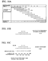
- an initial measurement point quantity table is produced in step S11. As shown in Fig. 14A, the initial measurement point quantity table defines the number of measurement points at respective magnification factors used in the scanning electron microscope 100. Determination of the number of measurement points is executed by use of the method described in this embodiment.
- step S12 the initial measurement point quantity obtained in step S11 as an operational measurement point quantity used in the line-width measurement.
- Fig. 14B shows an example of an operational measurement point quantity table.
- An optical axis of the scanning electron microscope 100 is adjusted in the next step S13.
- a standard line width Wr is obtained in the next step S14.
- the standard line width Wr is used as a judging standard as to whether or not the scanning electron microscope functions normally at the time of actual line-width measurement.
- the standard line width Wr is determined by measuring a standard measurement target at predetermined standard magnification (such as a 50,000-fold magnification) while using the initial measurement point quantity table.
- Fig. 14C shows an example of a standard line width table. Fig. 14C shows that the standard line width Wr obtained at the 50000-fold magnification is equal to 210 nm.
- a line profile data Dp representing a surface condition of a sample at the standard magnification are acquired by use of the standard measurement target used for determination of the operational standard value.
- the time of acquisition of the line profile data Dp will be defined as T1.
- a line width W1 is derived from the line profile data Dp acquired in step S21 while using the initial measurement point quantity table.
- the line width W1 obtained in step S22 is compared with the standard line width Wr. Specifically, the standard measurement target is measured at the standard magnification and the line width is determined by using the initial measurement points. Then, the judgment is made as to whether or not the line width falls within a predetermined acceptable error range as a consequence.
- the predetermined acceptable error range is defined as a difference in the line width within 0.4 nm, for example. If the line width does not fall within the predetermined acceptable error range, the line width cannot be used as the standard value. In this case, the process goes to step S29 and the operational standard value is set up again. When the line width is judged to be within the predetermined acceptable error range, the process goes to step S24.
- a line width W2 is derived from the line profile data Dp while using the operational measurement point quantity table.
- the line width W2 is compared with the standard line width Wr and a judgment is made as to whether or not a difference between the line width W2 and the standard line width Wr falls within another predetermined acceptable error range.
- This predetermined acceptable error range is defined as a difference in the line width within 0.2 nm, for example.
- the process goes to step S26 when the line width falls within the predetermined acceptable error range or the process goes to step 30 when the line width does not fall within the predetermined acceptable error range.
- the line profile data for the sample for measurement are acquired and the line width is measured by use of the operational measurement point quantity table.
- the time of acquisition of the line profile data will be defined as T2.
- step S27 the time period from the point of starting the operation to the point of measuring the sample for measurement is counted and a judgment is made as to whether or not the measured time period is longer than a predetermined period of time such as 24 hours.
- a predetermined period of time such as 24 hours.
- next step S28 a judgment is made as to whether or not the entire measurement of the line width is completed.
- the process is terminated.
- the judgment of completion of the line-width measurement may be determined by presence of a notice for completion of the measurement to be issued by a user operating a button or the like. If the line-width measurement is not completed, then the process returns to step S26 to continue the measurement.
- step S30 When the line width W2 determined by use of the operational measurement point quantity table does not fall within the acceptable error range as a result of comparison with the standard value in step S25, the process goes to step S30.
- the value on the operational measurement quantity table is adjusted in step S30. Since the operational standard value has been proved to be applicable in step S23, the number of operational measurement points is slightly adjusted to an applicable value in step S30. For example, if the line width W2 is greater than the standard line width Wr, the number of measurement points at the same magnification as the standard magnification is decremented by 0.1. On the other hand, if the line width W2 is smaller than the standard line width Wr, the number of measurement points at the same magnification as the standard magnification is incremented by 0.1. Regarding the magnification other than the standard magnification, the number of measurement points is derived from the number of measurement points at the standard magnification in accordance with the method described in this embodiment.
- the pitch of such increment or decrement is not limited only to this value.
- the allowable time lapse of the sample is set within 24 hours for avoiding the condition change in step S27, this allowance can also be changed as appropriate.
- the acceptable error range can also be changed as appropriate.
- the electron beam intensity distribution is adjusted so as to equalize the electron beam intensity distribution representing the distribution of the electron beam irradiated for each value of the scanning travel distance. In this way, even when the line width is measured while rescaling the magnification of observation, the distance of the electron beam irradiation in the scanning direction becomes substantially equal to the standard distance. Consequently, it is possible to prevent fluctuation in the measurement result of the line width.
- the distances of irradiation of the electron beams are equalized to the standard distance by adjusting the electron beam intensity distribution. Accordingly, it is possible to prevent different measurement results between the scanning electron microscopes in terms of the same line width of the pattern.
- the distance of irradiation of the electron beam is equalized to the standard distance by adjusting the electron beam intensity distribution. Accordingly, it is possible to prevent different measurement results depending on the scanning direction in terms of the same line width of the pattern.
Landscapes
- Physics & Mathematics (AREA)
- General Physics & Mathematics (AREA)
- Chemical & Material Sciences (AREA)
- Analytical Chemistry (AREA)
- Health & Medical Sciences (AREA)
- Life Sciences & Earth Sciences (AREA)
- Electromagnetism (AREA)
- Biochemistry (AREA)
- General Health & Medical Sciences (AREA)
- Immunology (AREA)
- Pathology (AREA)
- Length-Measuring Devices Using Wave Or Particle Radiation (AREA)
- Electron Sources, Ion Sources (AREA)
- Electron Beam Exposure (AREA)
- Analysing Materials By The Use Of Radiation (AREA)
Applications Claiming Priority (1)
| Application Number | Priority Date | Filing Date | Title |
|---|---|---|---|
| JP2006084868A JP4074643B2 (ja) | 2006-03-27 | 2006-03-27 | 線幅測定調整方法及び走査型電子顕微鏡 |
Publications (2)
| Publication Number | Publication Date |
|---|---|
| EP1840538A2 true EP1840538A2 (de) | 2007-10-03 |
| EP1840538A3 EP1840538A3 (de) | 2009-07-22 |
Family
ID=38191866
Family Applications (1)
| Application Number | Title | Priority Date | Filing Date |
|---|---|---|---|
| EP07005712A Withdrawn EP1840538A3 (de) | 2006-03-27 | 2007-03-20 | Zeilenbreiten-Messeinstellungsverfahren und Rasterelektronenmikroskop |
Country Status (4)
| Country | Link |
|---|---|
| US (1) | US7663103B2 (de) |
| EP (1) | EP1840538A3 (de) |
| JP (1) | JP4074643B2 (de) |
| KR (1) | KR100865593B1 (de) |
Cited By (1)
| Publication number | Priority date | Publication date | Assignee | Title |
|---|---|---|---|---|
| CN102901616A (zh) * | 2011-07-28 | 2013-01-30 | 中国计量科学研究院 | 一种激光线宽测量方法和设备 |
Families Citing this family (4)
| Publication number | Priority date | Publication date | Assignee | Title |
|---|---|---|---|---|
| US7772571B2 (en) * | 2007-10-08 | 2010-08-10 | Advanced Ion Beam Technology, Inc. | Implant beam utilization in an ion implanter |
| KR102441581B1 (ko) | 2015-06-03 | 2022-09-07 | 삼성전자주식회사 | 표면 검사 방법 및 이를 이용한 포토 마스크의 검사 방법 |
| WO2021140866A1 (ja) * | 2020-01-10 | 2021-07-15 | 株式会社ニューフレアテクノロジー | パターン検査装置及びパターン検査方法 |
| JP7793293B2 (ja) * | 2021-02-08 | 2026-01-05 | キヤノン株式会社 | 画像処理装置、画像処理装置の制御方法およびプログラム |
Citations (2)
| Publication number | Priority date | Publication date | Assignee | Title |
|---|---|---|---|---|
| US20010035495A1 (en) * | 2000-03-24 | 2001-11-01 | Kouichi Nagai | Scanning electron microscope and method of controlling the same |
| US20050205780A1 (en) | 2004-03-16 | 2005-09-22 | Ryo Nakagaki | Scanning electron microscope and a method for evaluating accuracy of repeated measurement using the same |
Family Cites Families (7)
| Publication number | Priority date | Publication date | Assignee | Title |
|---|---|---|---|---|
| US4038543A (en) * | 1975-07-08 | 1977-07-26 | Siemens Aktiengesellschaft | Scanning transmission electron microscope including an improved image detector |
| JPH05296754A (ja) | 1992-04-17 | 1993-11-09 | Nikon Corp | エッジ検出方法 |
| JPH09184714A (ja) | 1995-12-28 | 1997-07-15 | Hitachi Ltd | パターン寸法測定方法 |
| JP3420037B2 (ja) * | 1997-09-17 | 2003-06-23 | 株式会社東芝 | 寸法測定装置及び寸法測定方法 |
| US6476388B1 (en) * | 1998-10-19 | 2002-11-05 | Hitachi, Ltd. | Scanning electron microscope having magnification switching control |
| JP3743319B2 (ja) * | 2001-07-18 | 2006-02-08 | 株式会社日立製作所 | 欠陥検出方法及びその装置 |
| US7235799B2 (en) * | 2003-11-28 | 2007-06-26 | Ebara Corporation | System and method for evaluation using electron beam and manufacture of devices |
-
2006
- 2006-03-27 JP JP2006084868A patent/JP4074643B2/ja not_active Expired - Lifetime
-
2007
- 2007-03-20 EP EP07005712A patent/EP1840538A3/de not_active Withdrawn
- 2007-03-23 US US11/726,966 patent/US7663103B2/en active Active
- 2007-03-26 KR KR1020070029451A patent/KR100865593B1/ko not_active Expired - Fee Related
Patent Citations (2)
| Publication number | Priority date | Publication date | Assignee | Title |
|---|---|---|---|---|
| US20010035495A1 (en) * | 2000-03-24 | 2001-11-01 | Kouichi Nagai | Scanning electron microscope and method of controlling the same |
| US20050205780A1 (en) | 2004-03-16 | 2005-09-22 | Ryo Nakagaki | Scanning electron microscope and a method for evaluating accuracy of repeated measurement using the same |
Cited By (1)
| Publication number | Priority date | Publication date | Assignee | Title |
|---|---|---|---|---|
| CN102901616A (zh) * | 2011-07-28 | 2013-01-30 | 中国计量科学研究院 | 一种激光线宽测量方法和设备 |
Also Published As
| Publication number | Publication date |
|---|---|
| EP1840538A3 (de) | 2009-07-22 |
| US20070284525A1 (en) | 2007-12-13 |
| KR100865593B1 (ko) | 2008-10-27 |
| JP2007263566A (ja) | 2007-10-11 |
| US7663103B2 (en) | 2010-02-16 |
| JP4074643B2 (ja) | 2008-04-09 |
| KR20070096959A (ko) | 2007-10-02 |
Similar Documents
| Publication | Publication Date | Title |
|---|---|---|
| JP5103219B2 (ja) | パターン寸法計測方法 | |
| US7590506B2 (en) | Pattern measurement apparatus and pattern measuring method | |
| US11133148B2 (en) | Scanning electron microscope | |
| US8214166B2 (en) | Method and its system for calibrating measured data between different measuring tools | |
| US8357897B2 (en) | Charged particle beam device | |
| US8330104B2 (en) | Pattern measurement apparatus and pattern measurement method | |
| US20050285034A1 (en) | Method and apparatus for measuring three-dimensional shape of specimen by using SEM | |
| US8604431B2 (en) | Pattern-height measuring apparatus and pattern-height measuring method | |
| US20120032077A1 (en) | Pattern measuring apparatus and pattern measuring method | |
| US8431895B2 (en) | Pattern measuring apparatus and pattern measuring method | |
| JP4231798B2 (ja) | 荷電粒子線装置および倍率計測法 | |
| JPWO2017179138A1 (ja) | パターン計測装置およびパターン計測方法 | |
| US7408154B2 (en) | Scanning electron microscope, method for measuring a dimension of a pattern using the same, and apparatus for correcting difference between scanning electron microscopes | |
| EP1840538A2 (de) | Zeilenbreiten-Messeinstellungsverfahren und Rasterelektronenmikroskop | |
| US8263935B2 (en) | Charged particle beam apparatus | |
| KR20190138736A (ko) | 패턴 측정 방법, 패턴 측정 툴, 및 컴퓨터 가독 매체 | |
| KR102444526B1 (ko) | 전자 현미경 장치, 전자 현미경 장치를 이용한 검사 시스템 및 전자 현미경 장치를 이용한 검사 방법 | |
| JP2019027841A (ja) | 荷電粒子線装置 | |
| JP4812318B2 (ja) | 走査型電子顕微鏡を用いたパターン寸法の計測方法 | |
| US20030197873A1 (en) | Shape measurement method and apparatus | |
| KR102278301B1 (ko) | 하전 입자선 장치 | |
| US6969853B2 (en) | Pattern width measuring apparatus, pattern width measuring method, and electron beam exposure apparatus | |
| US11355304B2 (en) | Electronic microscope device | |
| EP3142139B1 (de) | Teilchenstrahlsystem und messverfahren | |
| WO2021149117A1 (ja) | 荷電粒子線画像用解析装置、検査システムおよびプログラム |
Legal Events
| Date | Code | Title | Description |
|---|---|---|---|
| PUAI | Public reference made under article 153(3) epc to a published international application that has entered the european phase |
Free format text: ORIGINAL CODE: 0009012 |
|
| 17P | Request for examination filed |
Effective date: 20070320 |
|
| AK | Designated contracting states |
Kind code of ref document: A2 Designated state(s): AT BE BG CH CY CZ DE DK EE ES FI FR GB GR HU IE IS IT LI LT LU LV MC MT NL PL PT RO SE SI SK TR |
|
| AX | Request for extension of the european patent |
Extension state: AL BA HR MK YU |
|
| PUAL | Search report despatched |
Free format text: ORIGINAL CODE: 0009013 |
|
| AK | Designated contracting states |
Kind code of ref document: A3 Designated state(s): AT BE BG CH CY CZ DE DK EE ES FI FR GB GR HU IE IS IT LI LT LU LV MC MT NL PL PT RO SE SI SK TR |
|
| AX | Request for extension of the european patent |
Extension state: AL BA HR MK RS |
|
| 17Q | First examination report despatched |
Effective date: 20090902 |
|
| AKX | Designation fees paid |
Designated state(s): DE FR IT |
|
| RIC1 | Information provided on ipc code assigned before grant |
Ipc: G01B 15/04 20060101AFI20120817BHEP Ipc: G01N 23/225 20060101ALI20120817BHEP Ipc: G01B 15/00 20060101ALI20120817BHEP |
|
| GRAP | Despatch of communication of intention to grant a patent |
Free format text: ORIGINAL CODE: EPIDOSNIGR1 |
|
| INTG | Intention to grant announced |
Effective date: 20160330 |
|
| STAA | Information on the status of an ep patent application or granted ep patent |
Free format text: STATUS: THE APPLICATION IS DEEMED TO BE WITHDRAWN |
|
| 18D | Application deemed to be withdrawn |
Effective date: 20160810 |