EP1840633A1 - Dispositif optique à guide d'ondes - Google Patents
Dispositif optique à guide d'ondes Download PDFInfo
- Publication number
- EP1840633A1 EP1840633A1 EP07005365A EP07005365A EP1840633A1 EP 1840633 A1 EP1840633 A1 EP 1840633A1 EP 07005365 A EP07005365 A EP 07005365A EP 07005365 A EP07005365 A EP 07005365A EP 1840633 A1 EP1840633 A1 EP 1840633A1
- Authority
- EP
- European Patent Office
- Prior art keywords
- waveguide
- branching
- substrate
- face
- optical
- Prior art date
- Legal status (The legal status is an assumption and is not a legal conclusion. Google has not performed a legal analysis and makes no representation as to the accuracy of the status listed.)
- Withdrawn
Links
Images


Classifications
-
- G—PHYSICS
- G02—OPTICS
- G02F—OPTICAL DEVICES OR ARRANGEMENTS FOR THE CONTROL OF LIGHT BY MODIFICATION OF THE OPTICAL PROPERTIES OF THE MEDIA OF THE ELEMENTS INVOLVED THEREIN; NON-LINEAR OPTICS; FREQUENCY-CHANGING OF LIGHT; OPTICAL LOGIC ELEMENTS; OPTICAL ANALOGUE/DIGITAL CONVERTERS
- G02F1/00—Devices or arrangements for the control of the intensity, colour, phase, polarisation or direction of light arriving from an independent light source, e.g. switching, gating or modulating; Non-linear optics
- G02F1/01—Devices or arrangements for the control of the intensity, colour, phase, polarisation or direction of light arriving from an independent light source, e.g. switching, gating or modulating; Non-linear optics for the control of the intensity, phase, polarisation or colour
- G02F1/03—Devices or arrangements for the control of the intensity, colour, phase, polarisation or direction of light arriving from an independent light source, e.g. switching, gating or modulating; Non-linear optics for the control of the intensity, phase, polarisation or colour based on ceramics or electro-optical crystals, e.g. exhibiting Pockels effect or Kerr effect
- G02F1/035—Devices or arrangements for the control of the intensity, colour, phase, polarisation or direction of light arriving from an independent light source, e.g. switching, gating or modulating; Non-linear optics for the control of the intensity, phase, polarisation or colour based on ceramics or electro-optical crystals, e.g. exhibiting Pockels effect or Kerr effect in an optical waveguide structure
- G02F1/0356—Devices or arrangements for the control of the intensity, colour, phase, polarisation or direction of light arriving from an independent light source, e.g. switching, gating or modulating; Non-linear optics for the control of the intensity, phase, polarisation or colour based on ceramics or electro-optical crystals, e.g. exhibiting Pockels effect or Kerr effect in an optical waveguide structure controlled by a high-frequency electromagnetic wave component in an electric waveguide structure
-
- G—PHYSICS
- G02—OPTICS
- G02F—OPTICAL DEVICES OR ARRANGEMENTS FOR THE CONTROL OF LIGHT BY MODIFICATION OF THE OPTICAL PROPERTIES OF THE MEDIA OF THE ELEMENTS INVOLVED THEREIN; NON-LINEAR OPTICS; FREQUENCY-CHANGING OF LIGHT; OPTICAL LOGIC ELEMENTS; OPTICAL ANALOGUE/DIGITAL CONVERTERS
- G02F1/00—Devices or arrangements for the control of the intensity, colour, phase, polarisation or direction of light arriving from an independent light source, e.g. switching, gating or modulating; Non-linear optics
- G02F1/01—Devices or arrangements for the control of the intensity, colour, phase, polarisation or direction of light arriving from an independent light source, e.g. switching, gating or modulating; Non-linear optics for the control of the intensity, phase, polarisation or colour
- G02F1/21—Devices or arrangements for the control of the intensity, colour, phase, polarisation or direction of light arriving from an independent light source, e.g. switching, gating or modulating; Non-linear optics for the control of the intensity, phase, polarisation or colour by interference
- G02F1/225—Devices or arrangements for the control of the intensity, colour, phase, polarisation or direction of light arriving from an independent light source, e.g. switching, gating or modulating; Non-linear optics for the control of the intensity, phase, polarisation or colour by interference in an optical waveguide structure
- G02F1/2255—Devices or arrangements for the control of the intensity, colour, phase, polarisation or direction of light arriving from an independent light source, e.g. switching, gating or modulating; Non-linear optics for the control of the intensity, phase, polarisation or colour by interference in an optical waveguide structure controlled by a high-frequency electromagnetic component in an electric waveguide structure
Definitions
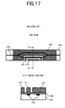
- the single-drive type LN modulator is user-friendly, and particularly, the chirp type LN modulator (FIG. 17) with chirps of a required amount, is advantageous in long-distance optical transmission, and this is widely used in long-distance, large-capacity optical transmission systems.
- the drive voltage required for obtaining the desired electro-optic effect can be reduced. Moreover, if it is assumed that the drive voltage is maintained constant, a length required for interaction between the light propagating in the optical waveguides and an electric signal propagating in the electrodes can be reduced. Accordingly, for example, when optical modulation is performed, modulation efficiency can be improved, and wideband modulation can be performed.
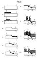
- FIG. 1 is a block diagram of a first embodiment of a waveguide-type optical device according to the present invention.
- the LN substrate 1 has an etching part 1A in which the height of one face (surface) of the substrate is made different from the height of other parts, in a preset portion positioned near the branching waveguide 13A of the optical waveguide 10 (a range enclosed by the broken line in the top view shown in the upper part of FIG. 1).
- the part excluding the etching part 1A, of the surface of the substrate becomes the first face (the face on an upper stage), and the part corresponding to the etching part 1A becomes the second face (the face on a lower stage).
- the buffer layer 30 is formed on the surface of the LN substrate 1 which is applied with the difference in level (S8). Then, a patterning process of the resist R is performed in order to form the signal electrode 21 and the ground electrode 22 on the buffer layer 30 (S9), and gold (Au) plating is applied on the buffer layer 30, with the resist as a mask (S10), and the resist R is then removed (S11). As a result, a drive electrode 20 of a predetermined pattern is formed with a signal electrode 21 arranged above the branching waveguide 13B, and a ground electrode 22 arranged above the branching waveguide 13A. An LN modulator having the etching part 1A as shown in FIG. 1 is then manufactured using an existing process technique.
- the example is shown where the etching part 1A is provided so that the position of the branching waveguide 13A on which the ground electrode 22 is arranged, is lower than the position of the branching waveguide 13B on which the signal electrode 21 is arranged.
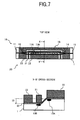
- the configuration may of course be such that an etching part 1 B is provided as shown in FIG. 7, so that the position of the branching waveguide 13B becomes lower than the position of the branching waveguide 13A.
- the etching parts 1A and 1B may be provided on a portion located on opposite sides of the branching waveguide 13B.
- the waveguide device of this embodiment is one where the function of the input waveguide 11 and the branching part 12, and the coupling part 14 and the output waveguide 15 formed in the LN substrate 1, is realized using optical fiber type couplers 41 and 41' to thereby simplify the configuration of the waveguide substrate.
- the branching waveguides 13A and 13B are formed near the face having a step of the LN substrate 1 on which the etching part 1E is formed.
- the height of the branching waveguide 13A is one stage lower than the height of the branching waveguide 13B.
- Opposite ends of the branching waveguides 13A and 13B extend as far as the end face of the LN substrate 1'.
- a ground electrode 22 is provided above the branching waveguide 13A via a buffer layer 30, and signal electrode 21 is provided above the branching waveguide 13B via the buffer layer 30.
- the optical fiber type coupler 41 on the input side has one input port and two branch ports. To the input port is input continuous light applied from the outside.
- the end face of one branch port is arranged near the input end face of the branching waveguide 13A, and the end face of the other branch port is arranged near the input end face of the branching waveguide 13B.
- the optical fiber type coupler 41' on the output side has two input ports, and one coupling port.
- One input port is arranged near the output end face of the branching waveguide 13A, and the end face of the other input port is arranged near the output end face of the branching waveguide 13B. From the coupling port is output light which is coupled light of the light input to the respective input ports.
- the input/output of light with respect to the branching waveguides 13A and 13B is performed using the optical fiber type couplers 41 and the 41'. Therefore, it is not necessary for the boundary portion positioned on the opposite ends of the etching portion to have a gradual slope shape as with the case of the first embodiment. Hence the step structure of the LN substrate 1 can be simplified, and the waveguide substrate can be easily manufactured.
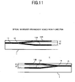
- the configuration example was shown using the optical fiber type couplers 41 and the 41'.
- the configuration may be such that light outgoing from an input optical fiber 51 is branched into two by a combination of lenses 52 and 54 and a prism 53, and guided to the input end faces of the respective branching waveguides 13A and 13B, and the light outgoing from the output end face of the respective branching waveguides 13A and 13B is combined by a combination of lenses 52' and 54' and a prism 53', and output from an output optical fiber 51'.
- FIG. 14 is a specific configuration example of the input side prism 53 shown in FIG. 13.
- the light outgoing from the input optical fiber 51 is made into parallel light by the lens 52, and this parallel light is branched into two by a half mirror 53A inside the prism 53.
- the light which has passed through the half mirror 53A is guided through the lens 54 to the input end face of the branching waveguide 13B, and the light which is reflected by the half mirror 53A is again reflected by a total reflection mirror 53B inside the prism 53 and then passes through the lens 54 and is focused onto the input end face of the branching waveguide 13A.
- the prism 53' on the output side is a similar configuration to the prism 53 on the input side, with the relationship of input and output reversed.
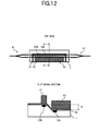
- FIG. 15 is a block diagram showing a fourth embodiment of a waveguide-type optical device according to the present invention.
- the waveguide-type optical device of this embodiment is one where the present invention is applied to a directional coupler type optical switch using a conventional Z-cut substrate.
- This directional coupler type optical switch comprises; a Z-cut LN substrate 1 ", an input waveguide 16, parallel waveguides 17A and 17B and output waveguides 18A and 18B, a signal electrode 21 and a ground electrode 22, and a buffer layer 30.
- the LN substrate 1" has a etching part 1 F in which the height of the substrate surface is made different from the height of other parts, in a preset portion positioned near the parallel waveguide 17B (a range enclosed by the broken line in the top view shown on the upper part of FIG. 15).
- the etching part 1 F gives a difference in level to the respective parallel waveguides 17A and 17B formed near the surface of the substrate 1".
- the difference in level is provided so that the height of the parallel waveguide 17B on which the ground electrode 22 is arranged, becomes lower than that of the parallel waveguide 17A on which the signal electrode 21 is arranged.
- the etching part 1 F has a slope shape at one end located on the output side in the longitudinal direction such that the difference in level gradually decreases from the end portion of the parallel waveguide 17B toward a middle part of the output waveguide 18B.
- the input waveguide 16, the parallel waveguides 17A and 17B, and the output waveguides 18A and 18B are respectively formed near the surface of the substrate by applying known processing such as titanium (Ti) diffusion with respect to the LN substrate 1" provided with the above etching part 1F.
- the parallel waveguide 17B has a position (height) one step lower than the other waveguide parts relative to the perpendicular direction of the substrate, due to the etching part 1 F of the LN substrate 1".
- the signal electrode 21 is provided above the parallel waveguide 17A via the buffer layer 30, and the ground electrode 22 is provided above the parallel waveguide 17B via the buffer layer 30.
- the optical signal applied from the outside to the input waveguide 16 is sent to the parallel waveguide 17A.
- the electric field generated between the signal electrode 21 and the ground electrode 22 acts on the pair of parallel waveguides 17A and 17B, corresponding to the control signal applied to one end of the signal electrode 21, and the state of the directional coupling of the light between the parallel waveguides 17A and 17B is controlled by the electro-optic effect due to the electric field.
- this acts as an optical switch where the optical signal sent from the input waveguide 16 to the parallel waveguide 17A is guided to either of the output waveguides 18A and 18B.
- the configuration example is shown using an LN substrate as the substrate having the electro-optic effect.
- the present invention is not limited to this, and it is possible to apply a known substrate having the electro-optic effect.
- the example is shown with an LN modulator and a directional coupler type optical switch.
- the present invention is effective for various types of waveguide-type optical switches which use a Z-cut substrate, with a signal electrode provided above one waveguide of a pair of waveguides, and a ground electrode provided above the other waveguide, and which are furnished with a function for controlling the state of light propagated on the pair of waveguides using the electro-optic effect due to an electric field generated between the signal electrode and the ground electrode.
Landscapes
- Physics & Mathematics (AREA)
- Nonlinear Science (AREA)
- Electromagnetism (AREA)
- General Physics & Mathematics (AREA)
- Optics & Photonics (AREA)
- Chemical & Material Sciences (AREA)
- Engineering & Computer Science (AREA)
- Ceramic Engineering (AREA)
- Crystallography & Structural Chemistry (AREA)
- Optical Integrated Circuits (AREA)
- Optical Modulation, Optical Deflection, Nonlinear Optics, Optical Demodulation, Optical Logic Elements (AREA)
Applications Claiming Priority (1)
| Application Number | Priority Date | Filing Date | Title |
|---|---|---|---|
| JP2006092979A JP2007264543A (ja) | 2006-03-30 | 2006-03-30 | 導波路型光デバイス |
Publications (1)
| Publication Number | Publication Date |
|---|---|
| EP1840633A1 true EP1840633A1 (fr) | 2007-10-03 |
Family
ID=38016438
Family Applications (1)
| Application Number | Title | Priority Date | Filing Date |
|---|---|---|---|
| EP07005365A Withdrawn EP1840633A1 (fr) | 2006-03-30 | 2007-03-15 | Dispositif optique à guide d'ondes |
Country Status (3)
| Country | Link |
|---|---|
| US (1) | US7373025B2 (fr) |
| EP (1) | EP1840633A1 (fr) |
| JP (1) | JP2007264543A (fr) |
Families Citing this family (3)
| Publication number | Priority date | Publication date | Assignee | Title |
|---|---|---|---|---|
| JP5158905B2 (ja) * | 2012-03-19 | 2013-03-06 | 古河電気工業株式会社 | 光回路基板およびその製造方法 |
| TW201426151A (zh) * | 2012-12-19 | 2014-07-01 | Hon Hai Prec Ind Co Ltd | 電光調製器 |
| JP2020134874A (ja) * | 2019-02-25 | 2020-08-31 | Tdk株式会社 | 光変調器 |
Citations (4)
| Publication number | Priority date | Publication date | Assignee | Title |
|---|---|---|---|---|
| JPH11295675A (ja) * | 1998-04-08 | 1999-10-29 | Nippon Telegr & Teleph Corp <Ntt> | 高速光変調器 |
| EP1258772A1 (fr) * | 2001-05-14 | 2002-11-20 | Corning O.T.I. S.p.A. | Modulateur électro-optique ayant une grande largeur de bande et une faible tension d'opération |
| WO2005029165A1 (fr) * | 2003-09-17 | 2005-03-31 | Ngk Insulators, Ltd. | Modulateur optique |
| US20050271313A1 (en) * | 2004-03-26 | 2005-12-08 | Sumitomo Osaka Cement Co., Ltd. | Optical device |
Family Cites Families (6)
| Publication number | Priority date | Publication date | Assignee | Title |
|---|---|---|---|---|
| JP2000266951A (ja) | 1999-03-16 | 2000-09-29 | Sumitomo Osaka Cement Co Ltd | 導波路型偏光子及びその形成方法 |
| US6324204B1 (en) * | 1999-10-19 | 2001-11-27 | Sparkolor Corporation | Channel-switched tunable laser for DWDM communications |
| JP3362126B2 (ja) * | 2000-03-09 | 2003-01-07 | 住友大阪セメント株式会社 | 光導波路素子 |
| JP2004219521A (ja) | 2003-01-10 | 2004-08-05 | Fuji Xerox Co Ltd | 導波路型光デバイス及びその製造方法 |
| US6876794B2 (en) * | 2003-02-10 | 2005-04-05 | Intel Corporation | Multi-waveguide layer H-tree distribution device |
| US7522783B2 (en) * | 2006-06-05 | 2009-04-21 | Fujitsu Limited | Optical interconnect apparatuses and electro-optic modulators for processing systems |
-
2006
- 2006-03-30 JP JP2006092979A patent/JP2007264543A/ja not_active Withdrawn
-
2007
- 2007-03-01 US US11/712,451 patent/US7373025B2/en not_active Expired - Fee Related
- 2007-03-15 EP EP07005365A patent/EP1840633A1/fr not_active Withdrawn
Patent Citations (4)
| Publication number | Priority date | Publication date | Assignee | Title |
|---|---|---|---|---|
| JPH11295675A (ja) * | 1998-04-08 | 1999-10-29 | Nippon Telegr & Teleph Corp <Ntt> | 高速光変調器 |
| EP1258772A1 (fr) * | 2001-05-14 | 2002-11-20 | Corning O.T.I. S.p.A. | Modulateur électro-optique ayant une grande largeur de bande et une faible tension d'opération |
| WO2005029165A1 (fr) * | 2003-09-17 | 2005-03-31 | Ngk Insulators, Ltd. | Modulateur optique |
| US20050271313A1 (en) * | 2004-03-26 | 2005-12-08 | Sumitomo Osaka Cement Co., Ltd. | Optical device |
Non-Patent Citations (1)
| Title |
|---|
| NAYYER J ET AL: "Modulation characteristics of high-speed optical modulators with properly split asymmetry into their Mach-Zehnder arms", ELECTRONICS LETTERS, IEE STEVENAGE, GB, vol. 31, no. 5, 2 March 1995 (1995-03-02), pages 387 - 388, XP006002518, ISSN: 0013-5194 * |
Also Published As
| Publication number | Publication date |
|---|---|
| JP2007264543A (ja) | 2007-10-11 |
| US20070286545A1 (en) | 2007-12-13 |
| US7373025B2 (en) | 2008-05-13 |
Similar Documents
| Publication | Publication Date | Title |
|---|---|---|
| JP3929814B2 (ja) | マッハ−ツェンダ電子−光学変調器 | |
| US7787717B2 (en) | Optical waveguide device | |
| EP3978993B1 (fr) | Élément de guide d'onde optique, et dispositif de modulation optique et appareil de transmission optique utilisant un élément de guide d'onde optique | |
| US8983239B2 (en) | Optical control element having a plurality of optical control portions | |
| EP1460458A1 (fr) | Guide d'ondes courbé à nervures, dispositif optique, et méthode de fabrication | |
| US6876782B2 (en) | Integrated type optical waveguide device | |
| US20050013522A1 (en) | Optical modulator with an impedance matching region | |
| US6700691B2 (en) | Electro-optic modulator having high bandwidth and low drive voltage | |
| JP5467414B2 (ja) | 光機能導波路 | |
| JPH07234391A (ja) | 光制御デバイス | |
| US20090162014A1 (en) | Optical waveguide device and optical apparatus using optical waveguide device | |
| JPH07318986A (ja) | 導波路型光スイッチ | |
| US7373025B2 (en) | Waveguide-type optical device | |
| EP1428067B1 (fr) | Procede et appareil de commutation et de modulation d'un signal optique avec une sensibilite accrue | |
| US8606053B2 (en) | Optical modulator | |
| JP3669999B2 (ja) | 光変調素子 | |
| JPWO2002023264A1 (ja) | 光デバイス | |
| JP4812476B2 (ja) | 光変調器 | |
| JP3164124B2 (ja) | 光スイッチ | |
| JP4701428B2 (ja) | 進行波型電極用の駆動回路、それを用いた光変調システム、光情報通信システム及び進行波型電極用の駆動方法 | |
| US7643712B2 (en) | Optical module and optical switching device | |
| JP2007033894A (ja) | 光変調器 | |
| WO2002093247A2 (fr) | Modulateur electro-optique | |
| JP2011112670A (ja) | マッハツェンダ光導波路とそれを用いた光変調器 |
Legal Events
| Date | Code | Title | Description |
|---|---|---|---|
| PUAI | Public reference made under article 153(3) epc to a published international application that has entered the european phase |
Free format text: ORIGINAL CODE: 0009012 |
|
| 17P | Request for examination filed |
Effective date: 20070713 |
|
| AK | Designated contracting states |
Kind code of ref document: A1 Designated state(s): AT BE BG CH CY CZ DE DK EE ES FI FR GB GR HU IE IS IT LI LT LU LV MC MT NL PL PT RO SE SI SK TR |
|
| AX | Request for extension of the european patent |
Extension state: AL BA HR MK YU |
|
| 17Q | First examination report despatched |
Effective date: 20071112 |
|
| AKX | Designation fees paid |
Designated state(s): DE FR GB |
|
| GRAP | Despatch of communication of intention to grant a patent |
Free format text: ORIGINAL CODE: EPIDOSNIGR1 |
|
| STAA | Information on the status of an ep patent application or granted ep patent |
Free format text: STATUS: THE APPLICATION IS DEEMED TO BE WITHDRAWN |
|
| 18D | Application deemed to be withdrawn |
Effective date: 20081230 |