EP1840722A2 - Flash-Speicher verwendendes Speichersystem, abnutzungsausgleichendes Verfahren für dieses System und abnutzungsausgleichendes Programm für dieses System - Google Patents
Flash-Speicher verwendendes Speichersystem, abnutzungsausgleichendes Verfahren für dieses System und abnutzungsausgleichendes Programm für dieses System Download PDFInfo
- Publication number
- EP1840722A2 EP1840722A2 EP06255786A EP06255786A EP1840722A2 EP 1840722 A2 EP1840722 A2 EP 1840722A2 EP 06255786 A EP06255786 A EP 06255786A EP 06255786 A EP06255786 A EP 06255786A EP 1840722 A2 EP1840722 A2 EP 1840722A2
- Authority
- EP
- European Patent Office
- Prior art keywords
- flash memory
- data
- wear
- leveling
- storage system
- Prior art date
- Legal status (The legal status is an assumption and is not a legal conclusion. Google has not performed a legal analysis and makes no representation as to the accuracy of the status listed.)
- Granted
Links
Images








Classifications
-
- G—PHYSICS
- G06—COMPUTING OR CALCULATING; COUNTING
- G06F—ELECTRIC DIGITAL DATA PROCESSING
- G06F12/00—Accessing, addressing or allocating within memory systems or architectures
- G06F12/02—Addressing or allocation; Relocation
- G06F12/0223—User address space allocation, e.g. contiguous or non contiguous base addressing
- G06F12/023—Free address space management
- G06F12/0238—Memory management in non-volatile memory, e.g. resistive RAM or ferroelectric memory
- G06F12/0246—Memory management in non-volatile memory, e.g. resistive RAM or ferroelectric memory in block erasable memory, e.g. flash memory
-
- G—PHYSICS
- G06—COMPUTING OR CALCULATING; COUNTING
- G06F—ELECTRIC DIGITAL DATA PROCESSING
- G06F2212/00—Indexing scheme relating to accessing, addressing or allocation within memory systems or architectures
- G06F2212/10—Providing a specific technical effect
- G06F2212/1032—Reliability improvement, data loss prevention, degraded operation etc
- G06F2212/1036—Life time enhancement
-
- G—PHYSICS
- G06—COMPUTING OR CALCULATING; COUNTING
- G06F—ELECTRIC DIGITAL DATA PROCESSING
- G06F2212/00—Indexing scheme relating to accessing, addressing or allocation within memory systems or architectures
- G06F2212/72—Details relating to flash memory management
- G06F2212/7208—Multiple device management, e.g. distributing data over multiple flash devices
-
- G—PHYSICS
- G06—COMPUTING OR CALCULATING; COUNTING
- G06F—ELECTRIC DIGITAL DATA PROCESSING
- G06F2212/00—Indexing scheme relating to accessing, addressing or allocation within memory systems or architectures
- G06F2212/72—Details relating to flash memory management
- G06F2212/7211—Wear leveling
-
- G—PHYSICS
- G06—COMPUTING OR CALCULATING; COUNTING
- G06F—ELECTRIC DIGITAL DATA PROCESSING
- G06F3/00—Input arrangements for transferring data to be processed into a form capable of being handled by the computer; Output arrangements for transferring data from processing unit to output unit, e.g. interface arrangements
- G06F3/06—Digital input from, or digital output to, record carriers, e.g. RAID, emulated record carriers or networked record carriers
- G06F3/0601—Interfaces specially adapted for storage systems
-
- G—PHYSICS
- G06—COMPUTING OR CALCULATING; COUNTING
- G06F—ELECTRIC DIGITAL DATA PROCESSING
- G06F3/00—Input arrangements for transferring data to be processed into a form capable of being handled by the computer; Output arrangements for transferring data from processing unit to output unit, e.g. interface arrangements
- G06F3/06—Digital input from, or digital output to, record carriers, e.g. RAID, emulated record carriers or networked record carriers
- G06F3/0601—Interfaces specially adapted for storage systems
- G06F3/0628—Interfaces specially adapted for storage systems making use of a particular technique
- G06F3/0662—Virtualisation aspects
- G06F3/0664—Virtualisation aspects at device level, e.g. emulation of a storage device or system
Definitions
- the present invention relates to a storage system using flash memories capable of wear-leveling among plural flash memory modules, a wear-leveling method for the storage system, and a wear-leveling program for the storage system.
- a system for storing data (hereinafter referred to as “storage system”) generally includes randomly accessible nonvolatile memory media.
- Randomly accessible nonvolatile memory media includes, for example, a magnetic disk or an optical disk. Recently, a common storage system has many compact disk drives.
- nonvolatile semiconductor memories have been developed, on which data can be erased at a time, such as a flash memory.
- a flash memory is a semiconductor memory that is a nonvolatile memory serving as a read only memory (ROM), as well as a random access memory (RAM) which is both readable and writable.
- ROM read only memory
- RAM random access memory
- a storage system having flash memories as storage media is excellent in service life, power-saving and access time, in comparison to a storage system having many small compact disk drives.
- a block denotes a unit of storage area where data is erased at a time.
- a flash memory for example, storage area where data has been erased is always set as “1". Therefore, it is possible to rewrite "1" to "0" by binary bit conversion when rewriting data. However, it is impossible to directly rewrite "0" to "1” unless stored data is erased. In order to rewrite data onto a flash memory, an entire block of the flash memory is erased. Accordingly, a flash memory always requires a block erase when data is rewritten onto the flash memory.
- a flash memory has limitation of block erase counts. For example, block erase counts are ensured up to 100,000 counts per block. If a specific block experiences excessive erase counts due to intensive data rewriting, it becomes impossible to erase data on the block any more, which causes a problem. Therefore, in a storage system using flash memories as storage media, it is essential to prepare a wear-leveling process to prevent intensive erase counts from occurring on a specific block.
- JP-A-8-16482 discloses a wear-leveling method in which a storage system employs a mapping management method for providing flexibility for a block association relationship between a host computer and flash memories to solve a problem that a physical block of a flash memory is selected one-sidedly by a logical block when a computer accesses to the logical block.
- this conventional storage system manages write counts of each logical block to which the host computer accesses, and erase counts of each physical block that the storage system erases.
- a mapping is provided in such a manner that the logical block having excessive write counts is allowed to correspond to the physical block having fewer erase counts, and the logical block having fewer write counts is allowed to correspond to the physical block having excessive erase counts.
- a flash memory module (hereinafter referred to as "PDEV") is constituted by a memory controller and plural flash memory chips, and the memory controller provides a wear-leveling process which is the same as that of the above mentioned conventional scheme.
- PDEV flash memory module
- the memory controller provides a wear-leveling process which is the same as that of the above mentioned conventional scheme.
- each flash memory is provided with wear-leveling by using the controller.
- wear-leveling among plural flash memory modules it is required to provide wear-leveling among plural flash memory modules.
- the storage system has to integrally manage erase counts of tremendous a number of physical blocks, resulting in increase in management loads and deterioration in performance of the storage system.
- a storage system using flash memories including a storage controller and plural flash memory modules as storage media.
- Each flash memory module includes at least one flash memory chip and a memory controller for leveling erase counts of blocks belonging to the flash memory chip.
- the storage controller combines the plural flash memory modules into a first logical group, translating a first address used for accessing the flash memory modules belonging to the first logical group to a second address used for handling the first address in the storage controller, and combining the plural first logical groups into a second logical group.
- a wear-leveling method for a storage system using flash memories including flash memory modules including at least one flash memory chip and a memory controller for leveling erase counts of blocks belonging to the flash memory chip; and a storage controller for combining the flash memory modules into a first logical group, translating a first address used for accessing the flash memory modules belonging to the first logical group to a second address used for handling the first address in the storage controller, and combining a plurality of first logical groups into a second logical group.
- the method includes a step of allowing the storage controller to provide count management on write size of each predetermined memory area in the flash memory module; a step of allowing the storage controller to calculate an average erase count yielded by dividing total write size of each flash memory module through a predetermined time period by a capacity of the flash memory module and a first determination step of allowing the storage controller to determine whether or not a difference between a maximum value and a minimum value of the average erase count is not less than a predetermined value.
- the method further includes a step of allowing the storage controller to exchange data between memory area having a maximum write size and memory area having a minimum write size, among the flash memory modules having the maximum difference of the erase count, and to change mapping information between the first address and the second address.
- a wear-leveling program for a storage system using flash memories including flash memory modules including at least one flash memory chip and a memory controller for leveling erase counts of blocks belonging to the flash memory chip; and a storage controller for combining the flash memory modules into a first logical group, translating a first address used for accessing the flash memory modules belonging to the first logical group to a second address used for handling the first address in the storage controller, and combining the plural first logical groups into a second logical group.
- the program performs a process for allowing a computer to provide count management on write size of each predetermined memory area in the flash memory module; a process for allowing the computer to calculate an average erase count yielded by dividing total write size of each flash memory module through a predetermined time period by capacity of the flash memory module; and a process of a first determination of allowing the computer to determine whether or not a difference between a maximum value and a minimum value of the average erase count is not less than a predetermined value. If the difference is not less than a predetermined value, the program further includes a process for allowing the computer to change mapping information between the first address and the second address.
- a storage system using flash memories includes a storage controller and plural flash memory modules as storage media.
- Each flash memory module e.g. flash memory module PO
- includes at least one flash memory chip e.g. flash memory chip 405), and a memory controller (e.g. controller MC) for leveling erase counts of blocks (e.g. block 406) belonging to the flash memory chip.
- the storage controller e.g. storage controller SC
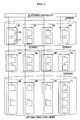
- FIG 1 is a block diagram showing a configuration of the storage system according to the present embodiment.
- the storage system 100 includes a storage controller SC and flash memory modules P00 to P35.
- the storage controller SC includes channel adapters CA0, CA1, cache memories CM0, CM1, storage adapters SA0, SA1, and interconnection networks NW0, NW1.
- channel adapters CA0, CA1, cache memories CM0, CM1, storage adapters SA0, SA1 are shown in pairs respectively in the drawing, those components are provided not limited to in pairs, but may be provided in numbers.
- the interconnection networks NW0, NW1 may be switches, and interconnect devices constituting the storage controller SC. Specifically, the interconnection networks NW0, NW1 interconnect the channel adapter CA0, the cache memory CM0 and the storage adapter SA0. The interconnection networks NW0, NW1 also interconnects the channel adapter CA1, the cache memory CM1 and the storage adapter SA1.
- the channel adapter CA0 is connected with an external host system (not shown) via the channels C00, C01, C02, C03.
- the channel adapter CA1 is connected with an external host system (not shown) via the channels C10, C11, C12, C13.
- a host system denotes a computer for reading and writing data onto the storage system 100 according to the present embodiment.
- the storage system 100 connects with a host system or other storage system via Fibre Channel switches, FC-AL (Fibre Channel Arbitrated Loop), SAS (Serial Attached SCSI) Expander, or the like.
- the cache memory CM0 temporarily stores data received from the channel adapter CA0 and the storage adapter SA0.
- the cache memory CM1 temporarily stores data received from the channel adapter CA1 and the storage adapter SA1.
- the storage adapter SA0 is connected with a flash memory module P00, etc. (described later in FIG 3). Specifically, the storage adapter SA0 is connected with flash memory modules P00 to P05 via a channel D00. The storage adapter SA0 is also connected with flash memory modules P10 to P15 via a channel D01. The storage adapter SA0 is further connected with flash memory modules P20 to P25 via a channel D02. Furthermore, the storage adapter SA0 is connected with flash memory modules P30 to P35 via a channel D03.
- the storage adapter SA1 is connected with flash memory module P00, etc. Specifically, the storage adapter SA1 is connected with flash memory modules P00 to P05 via a channel D10. The storage adapter SA1 is also connected with flash memory modules P10 to P15 via a channel D11 . The storage adapter SA1 is further connected with flash memory modules P20 to P25 via a channel D12. Furthermore, the storage adapter SA1 is connected with flash memory modules P30 to P35 via a channel D13. Specifically, the storage adapters and the flash memories modules are connected with each other via Fibre Channel switches, FC-AL, SAS Expander, or the like.
- the channel adapters CA0, CA1 and the storage adapters SA0, SA1 are connected with a maintenance terminal SVP.
- the maintenance terminal SVP sends setting information inputted by an administrator of the storage system 100 to the channel adapters CA0, CA1 and/or the storage adapters SAO, SA1.
- the storage system 100 may be equipped with a single adapter instead of using the storage adapter SA0 and the channel adapter CA0. In this case, this single adapter performs a process to be performed by the storage adapter SA0 and the channel adapter CA0.
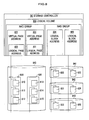
- FIG 2 is a block diagram showing a configuration of the channel adapter.
- the channel adapter CA0 includes a host channel interface 21, a cache memory interface 22, a network interface 23, a processor 24, a local memory 25 and a processor peripheral control unit 26.
- the host channel interface 21 is connected with an external host system (not shown) via the channels C00, C01, C02, C03.
- the host channel interface 21 inter-converts data transfer protocol on the channels C00, C01, C02, C03 to data transfer protocol inside the storage controller SC
- the cache memory interface 22 is connected with interconnection networks NW0, NW1.
- the network interface 23 is connected with the maintenance terminal SVP.
- the host channel interface 21 and the cache memory interface 22 connect with each other via signal lines 27.
- the processor 24 performs various processes by executing each of the programs stored on a local memory 25. Specifically, the processor 24 controls data transfer between a host system and the interconnection networks NW0, NW1.
- the local memory 25 stores the programs executed by the processor 24.
- the local memory 25 stores tables to be looked up by the processor 24. The tables may be set or changed by the administrator.
- the administrator inputs information on setting or change of the table.
- the maintenance terminal SVP sends the information inputted by the administrator to the processor 24 via the network interface 23.
- the processor 24 generates or changes a table based on the received information. Then, the processor 24 stores the table on the local memory 25.
- the processor peripheral control unit 26 controls data transfer among the host interface channel 21, the cache memory interface 22, the network interface 23, the processor 24 and the local memory 25.
- the processor peripheral control unit 26 is, for example, a chipset or the like.
- the channel adapter CA1 has the same configuration as that of the channel adapter CA0. Therefore an explanation on the channel adapter CA1 will be omitted herein.
- FIG 3 is a block diagram showing the storage adapter according to the present embodiment.
- the storage adapter SA0 includes a cache memory interface 31, a storage channel interface 32, a network interface 33, a processor 34, a local memory 35 and a processor peripheral control unit 36.
- the cache memory interface 31 is connected with the interconnection networks NW0, NW1.
- the storage channel interface 32 is connected with channels D00, D01, D02, D03.
- the storage channel interface 32 inter-converts a data transfer protocol on the channels D00, D01 D02, D03 and a data transfer protocol inside the storage controller SC to each other.
- the cache memory interface 31 and the storage channel interface 32 are connected with each other via the signal lines 37.
- the network interface 33 is connected with a maintenance terminal SVP.
- the processor 34 performs various processes by executing each program stored on the local memory 35.
- the local memory 35 stores the programs to be executed by the processor 34.
- the local memory 35 stores tables to be looked up by the processor 34, as well. The tables may be set or changed by the administrator.
- the administrator inputs information on setting or change of the tables into the maintenance terminal SVP.
- the maintenance terminal SVP sends the processor 34 the information inputted by the administrator via the network interface 33.
- the processor 34 generates or changes the tables based on the received information. Then, the processor 34 stores the table onto the local memory 35.
- the processor peripheral control unit 36 controls data transfer among the cache memory interface 31, the storage channel interface 32, the network interface 33, the processor 34 and the local memory 35.
- the processor peripheral control unit 36 may be a chipset or the like.
- the storage adapter SA1 has the same configuration as that of the storage adapter SA0. Therefore an explanation on the storage adapter SA1 will be omitted herein.
- FIG 4 is a block diagram showing a configuration of a flash memory module according to the present invention.
- a flash memory module P00 includes a memory controller MC and a flash memory MEM.
- the flash memory MEM stores data.
- the memory controller MC reads/writes or erases the data stored on the flash memory MEM.
- the memory controller MC includes a processor ( ⁇ P) 401, an interface unit (I/F) 402, a data transfer unit (HUB) 403, a memory (RAM) 404 and a memory (ROM) 407.
- ⁇ P processor
- I/F interface unit
- UOB data transfer unit
- RAM memory
- ROM memory
- the flash memory MEM includes plural flash memory chips 405.
- Each flash memory chip 405 includes plural blocks 406 to store data thereon.
- Each block 406 is a unit by which the memory controller MC erases data, as described later in FIG 5.
- the block 406 includes plural pages.
- a page is a unit by which the memory controller MC reads/writes data, as described later in FIG 5. Every page is categorized either in a valid page, an invalid page, an unused page, or a bad page.
- a valid page is a page storing valid data.
- An invalid page is a page storing invalid data.
- An unused page is a page storing no data.
- a bad page is a page physically unavailable, for example, because the page contains broken storage elements.
- the interface unit 402 is connected with the storage adapter SA0 in the storage controller SC via the channel D00.
- the interface unit 402 is also connected with the storage adapter SA1 in the storage controller SC via the channel D10.
- the interface unit 402 receives instructions from the storage adapter SA0 and the storage adapter SA1. Instructions from the storage adapter SA0 and the storage adapter SA1 are such as SCSI commands.
- the interface unit 402 receives data from the storage adapter SA0 and the storage adapter SA1. Then the interface unit 402 stores the received data onto the memory 404. The interface unit 402 also sends the data stored on the memory 404 to the storage adapter SA0 and the storage adapter SA1.
- the memory 404 is, for example, a dynamic RAM memory which can read/write data at high speed.
- the memory 404 temporarily stores data that is sent or received by the interface unit 402.
- the memory 407 is a nonvolatile memory for storing programs to be executed by the processor 401.
- flash memory module P00 When flash memory module P00 is activated, the program is copied from the memory 407 onto the memory 404 so that the processor 401 can execute the program.
- the memory 404 stores the tables to be looked up by the processor 401.
- the tables may include, for example, an address translation table between a logical page address and a physical page address of the flash memory MEM.
- the logical page address is an address for use when accessing from outside a flash memory module (for example, from the storage adapter SAO) to a page as a unit by which data is read/written onto a flash memory.
- a physical page address is an address for use when the memory controller MC accesses to a page serving as a unit by which data is read/written onto a flash memory.
- the data transfer unit 403 may be, for example, a switch for interconnecting a processor 401, an interface unit 402, a memory 404, a memory 407 and a flash memory MEM, and controls data transfer among these components.
- the processor 401 performs various processes by executing each of the programs stored on the memory 404. For example, the processor 401 looks up an address translation table between the logical page address and the physical page address of a flash memory, which is stored on the memory 404, and then reads/writes data onto the flash memory MEM based on the table. The processor 401 provides a reclamation process (block reclamation process) and a wear-leveling process for the block 406 in the flash memory module.
- a reclamation process block reclamation process
- wear-leveling process for the block 406 in the flash memory module.
- the reclamation process is a process to rebuild an invalid page in the block 406 into an unused page, so that a block having fewer unused pages can be rebuilt to be available again.
- the block 406 to be a target for the reclamation process includes valid pages, invalid pages and unused pages, and many of them are invalid pages. In this case, it is required to erase invalid pages in order to increase unused pages.
- an erasing process can be done not on a page by page basis, but on a block by block basis. Therefore, it is required to rebuild a block to be available in such a manner that a valid page of a target block is copied onto an empty block, and then a target block is erased.
- the processor 401 copies data stored on a valid page in the block 406 that is targeted for the reclamation process (i.e. target block) onto an unused block.
- the processor 401 changes a logical block number of the unused block on which data has been copied to a logical block number of the target block. Then, all the data on the target block is erased, whereby the reclamation process is completed.
- the processor 401 writes more data onto the block 406, more unused pages in the block 406 are decreased. Then, if the block 406 becomes in short of unused pages, the processor 401 cannot write data onto the block 406 any more. Therefore, the processor 401 reclaims an invalid page into an unused page by performing the reclamation process on the block 406.
- the wear-leveling process is a process for leveling erase counts of the block 406, whereby the flash memory MEM endurance can be increased.
- the flash memory MEM endurance is usually assured up to 10,000 to 100,000 counts.
- FIG 5 is a diagram showing a structure of a block of a flash memory module.
- the block 406 of the flash memory module P00 includes plural pages 501.
- the block 406 usually includes several ten pages 501 (e.g. 32 pages, 64 pages).
- Each page 501 is a unit by which the memory controller MC or the like reads/writes data.
- the memory controller MC or the like reads data at speed of 20 to 30 ⁇ s or less/page, and writes data at speed of 0.2 to 0.3 ms/page.
- the memory controller MC or the like erases data at speed of 2 to 4 ms/block.
- the page 501 includes a data section 502 and a redundant section 503.
- the data section 502 may comprise 512 bytes, and the redundant section 503 may comprise 16 bytes, for example.
- the data section 502 stores ordinal data.
- the redundant section 503 stores management information and an error correction code about the page 501.
- the management information includes offset addresses and page statuses.
- the offset address is a relative address in the block 406 to which the page 501 belongs.
- the page status shows whether the page 501 is a valid page, an invalid page, an unused page, or a page under being processed.
- the error correction code is a code to detect and correct an error on the page 501, such as Humming code.
- FIG 6 is a block diagram showing a structure of logical groups and a hierarchy of address translation.
- the storage system in FIG 6 has the same hardware configuration as that of the storage system in FIG 1. For the convenience, only the channels D00, D01, D02, D03 are shown, as the channels of the storage controller SC which connects with the flash memory modules P00 to P35, and the channels D10, D11, D12, D13 are omitted in the drawing.
- flash memory modules connected with one another on a same channel constitutes a wear-leveling group (WDEV).
- WDEV wear-leveling group
- the flash memory modules P00 to P03 on the channel D00 constitutes a wear-leveling group W00.
- Each flash memory module can be accessed via a corresponding logical page address thereof from the storage controller SC.
- the flash memory modules P00 to P03 on the channel D00 can be accessed via each corresponding logical page address 600 of the modules.
- the flash memory modules P10 to P13 on the channel D01 can be accessed via each corresponding logical page address 601 of the modules;
- the flash memory modules P20 to P23 on the channel D02 can be accessed via each corresponding logical page address 602 of the modules;
- the flash memory modules P30 to P33 on the channel D03 can be accessed via each corresponding logical page address 603 of the modules.
- the storage controller SC puts plural logical page addresses of flash memory modules belonging to a same wear-leveling group together into a group and translates the group into a single virtual page address. For example, the storage controller SC puts the logical page addresses 600 of the flash memory modules P00 to P03 belonging to the wear-leveling group W00 together, and translates the group into a virtual page address 604.
- the logical page addresses 601 of the flash memory modules P10 to P13 belonging to a wear-leveling group W10 are put together and translated into a virtual page address 605;
- the logical page addresses 602 of the flash memory modules P20 to P23 belonging to a wear-leveling group W20 are put together and translated into a virtual page address 606;
- the logical page addresses 603 of the flash memory modules P30 to P33 belonging to a wear-leveling group W30 are put together and translated into a virtual page address 607.
- the storage controller SC translates a logical page address into a virtual page address. In this way, even if data is transferred between flash memory modules for the sake of wear-leveling and a related logical page address is changed, the storage controller SC that is a higher-level device can change a mapping between a logical page address and a virtual page address corresponding to the logical address, so that data can be accessed with no conflicts.
- plural wear-leveling groups are combined so as to constitute a single RAID group (VDEV).
- VDEV RAID group
- four wear-leveling groups W00 to W30 are combined into a RAID group V00.
- Each virtual page address page area in each of the wear-leveling groups constituting a single RAID group has the same storage capacity.
- Areas in one or more RAID groups are combined into a single logical volume 608, which is memory area that the storage controller SC shows to a host system.
- Flash memory modules P04, P05 on the channel D00 constitute a spare group (YDEV) Y00.
- FIG 7 is a block diagram showing a structure of RAID groups of the storage system 100 according to the present embodiment.
- a RAID group 720 is a RAID group on RAID level 5, which is constituted by wear-leveling groups 700 to 703.
- the wear-leveling 700 is constituted by flash memory modules 730, 731.
- a RAID is classified in to a level, such as RAID level 0 or RAID level 1, and so on, depending on a function thereof.
- a RAID group 721 is a RAID group on RAID level 1 constituted by wear-leveling groups 704, 705.
- a RAID group 722 is a RAID group on RAID level 1 constituted by wear-leveling groups 706, 707
- a RAID is classified into levels 0, 1, 3, 5, 6 or 1+0, equal capacity is provided for logical page address area of each of the wear-leveling groups constituting a same RAID group.
- An upper limit of wear-leveling group capacity is defined by Formula 1, and a lower limit thereof is defined by Formula 2.
- a product of "sustained write speed of a flash memory module” and “system endurance” divided by “flash memory endurance” yields a second value (upper limit).
- a product of "effective write speed of a flash memory module while the system is being operated” and “system endurance” divided by “flash memory endurance” yields a first value (lower limit).
- capacity of logical page address area of each wear-leveling group is set to be not less than the first value and not more than the second value.
- system endurance is usually from 5 to 10 years
- flash memory endurance is usually from 10, 000 to 100, 000 counts.
- Effective write speed in the Formula 2 denotes effective write speed in consideration of write access ratio from a host system to the storage system 100.
- Upper Limit Sustained Write Speed Module ⁇ System Endurance Flash Memory Endurance
- Wear - leveling Group Capacity Value ( Lower Limit ) Effective Write Speed per Module ⁇ System Endurance Flash Memory Endurance
- Capacity of the wear-leveling group is set to fall in a range defined by Formula 1 and Formula 2.
- a RAID group 723 is a RAID group on RAID level 4 constituted by wear-leveling groups 708 to 711; and the wear-leveling groups 708 to 710 are wear-leveling groups for storing data; and the wear-leveling group 711 is a wear-leveling group for storing parities.
- the wear-leveling group for storing parities has more updating counts than those of other wear-leveling groups for storing data. Therefore, in order to provide a wear-leveling process in a RAID group on RAID level 4, capacity of the logical page address area in the wear-leveling group for storing parities is set to be larger than that of the logical page address area in the wear-leveling group for storing data.
- capacity of the logical page address area of the wear-leveling group for storing parities is set to be not less than one time and not more than (n-1) times as much as that of wear-leveling groups for storing data.
- wear-leveling groups for storing redundant information have more update counts than those of wear-leveling groups for storing data.
- each RAID group in the storage controller SC is constituted by combining wear-leveling groups.
- the storage controller SC manages each RAID group in consideration of wear-leveling groups thereof. Therefore, a virtual page address of each wear-leveling group is deemed as independent, regardless of a mapping between a logical page address and a virtual page address in each wear-leveling group. Accordingly, the storage controller SC can connect plural RAID groups on different levels with one another.
- FIG 8 is a block diagram showing an example in which flash memory modules and hard disk drives are connected with the storage controller SC.
- Flash memory modules 810 to 812 constitute a wear-leveling group 830.
- Flash memory modules 813 to 815 constitute a wear-leveling group 831, and the wear-leveling groups 830, 831 constitute a RAID group 840.
- the storage controller SC translates logical page address 800 into a virtual page address 802 so as to access to either one of the flash memory modules 810 to 812.
- the storage controller SC also translates a logical page address 801 into a virtual page address 803 so as to access to either one of the flash memory modules 813 to 815.
- Hard disk drives 820 and 823 are combined into a RAID group 841. Similarly, hard disk drives 821 and 824 are combined into a RAID group 842; and hard disk drives 822 and 825 are combined into a RAID group 843.
- the storage controller SC accesses to each hard disk drive via the logical block address 804 or 805. In a RAID group constituted by hard disk drives, no wear-leveling groups are defined because no wear-leveling is needed.
- the storage controller SC defines wear-leveling groups only in a RAID group constituted by flash memory modules, and translates a logical page address into a virtual page address.
- the storage controller SC When the system is activated or storage media is connected with the system, the storage controller SC changes control on determination of whether or not any address translation is necessary, or determination of how to configure a RAID group, etc., depending on whether the storage media is flash memories or hard disk drives.
- the storage controller SC constitutes a logical volume 808 by using either area of the RAID group 840 constituted by flash memory modules or the RAID groups 841 to 843 constituted by hard disk drives, or by combining areas of the RAID group 840 and the RAID groups 841 to 843.
- How to choose storage area of flash memory modules or storage area of hard disk drives may be such that data having more read accesses and less update counts is stored on flash memory modules, and data having more update counts is stored on hard disk drives. Flash memory modules can access to hard disk drives with law latency. Therefore, if storage area is chosen depending on access property of storage media, as described above, high performance for the storage system can be realized.
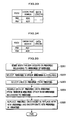
- FIG 9 is a flow chart showing a wear-leveling process among plural flash memory modules. To be simplified, it is assumed that a target wear-leveling group W00 has two flash memory modules P00, P04.
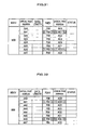
- FIG 10 shows an address translation table between a virtual page address and a logical page address before a data exchange process accompanied by the wear-leveling process according to the present embodiment.
- FIG 11 shows the address translation table between the virtual page address and the logical page address after the data exchange accompanied by the wear-leveling process according to the present embodiment.
- mappings between the virtual page address and the logical page address are indicated, as well as offset values for the mappings.
- a logical page address area (data length) is set to be larger than a corresponding virtual page address area (data length).
- an offset value "0" is indicated if a valid data is written on a start address side and free area exists on an end address side.
- An offset value "1" is indicated if a valid data is written on an end address side and free area exists on a start address side.
- free area has a size that is an integral multiple (at least one time) of a data section of a flash memory page, and that is equal to data size that a memory controller in a flash memory module can read/write onto a flash memory at a time.
- FIG 12 shows an erase count management table for each flash memory module, which is managed by the storage controller SC.
- the storage controller SC records a total write size of each area serving as a unit for data exchange within a flash memory module.
- an average erase count of flash memories in the flash memory module can be obtained by adding a previous average erase count value to an average process count yielded by dividing a sum of an individual total write size of each logical page address area of a module in a separate predetermined time period by an entire logical page address area capacity of the module (module capacity).
- Formula 3 Average Erase Count Previous Value + ⁇ Sum of Individual Total Write Size of Each Logiciel Page Address Area of a Module in a Seperate Predetermined Time Period Module Capacity
- a moving flag is set in such a manner that the flag is set to be "0" before the data exchange process, and the flag is set to be "1" after the data exchange process.
- the total write size is managed in each separate time period. Providing no separate predetermined time period, the total write size through the entire time period can be represented by Formula 4. Either result from Formula 3 or Formula 4 yields the same average erase count value.
- Formula 4 Average Erase Count ⁇ Sum of Individual Total Write Size of Each Logical Page Address Area of a Module through Entire Predetermined Time Period Module Capacity
- the address translation tables shown in FIG 10 or FIG 11 and an average erase count management table in FIG 12 are required to be maintained even when a failure occurs such as a power failure or when it is out of the system service time. Therefore, the storage controller SC stores, on each predetermined area of each flash memory module, data related to the address translation table, and the average erase count management table for each module.
- the storage controller SC performs the wear-leveling process when an event occurs, for example, every time total write size of any wear-leveling group (WDEV) reaches a predetermined value, or in every predetermined time period. At this time, the storage controller SC sets a moving flag of the flash memory module in the wear-leveling group to be "0" (S901) .
- the storage controller SC checks that the moving flag is set to "0", and a maximum value and a minimum value of the average erase count, by looking up the average erase count management table of FIG 12 (S902).
- the storage controller SC determines whether or not a difference between the maximum value and the minimum value of the average erase count is not less than a predetermined value (S903). If the difference of the erase count is not less than the predetermined value, the storage controller SC proceeds to S904. If the difference of the erase count is less than the predetermined value, the storage controller SC completes the process.
- the storage controller SC selects a logical page address area having a maximum total write size in a flash memory module (PDEV) having a maximum average erase count; and a logical page address having a minimum total write size in the flash memory module (PDEV) having a minimum average erase count (S904).
- PDEV flash memory module
- S904 minimum average erase count
- the storage controller SC sets a status field of the address translation table of FIG 10 between a virtual page and a logical page as "exchanging". Specifically, the storage controller SC inputs a value indicating "exchanging" into the status field of the translation table of FIG 10, in order to perform data exchange between two selected logical page address areas and change mapping with corresponding virtual page addresses (S905). The storage controller SC temporarily stays on standby in accessing to storage area on which "exchanging" is indicated, and tries an access again to the storage area after the data exchange operation and the mapping change operation are completed. During this process, data written from a host system is stored on cache memories in the storage controller SC.
- the storage controller SC exchanges data between the above two logical page address areas (S906). A detailed description on the data exchange process will be given later.
- the storage controller SC updates a current average erase count value in a field of a flash memory module (PDEV) to which the data exchange target area belongs, where the previous average erase count value has been recorded, and clears the total write size (S907). Accordingly, the average erase count value immediately after the data exchange operation is identical to the previous average erase count value.
- PDEV flash memory module
- the storage controller SC changes the mapping and the offset value between the virtual page address and the logical page address, and clears the status field, and then sets the moving flag to be "1" (S908).
- the wear-leveling group W00 to be a target for wear-leveling includes two flash memory modules P00, P04. Therefore, if there is performed any data exchange between the flash memory modules P00, P04, the moving flags of the flash memory modules P00, P04 are both set to be "1".
- the storage controller SC determines whether or not there are plural flash memory modules (PDEV) having moving flags of "0" (S909). If it is determined that there area no plural flash memory modules having moving flags of "0”, the storage controller SC completes the wear-leveling process. If it is determined there are any plural flash memory modules having moving flags of "0", the storage controller SC returns to S902. In FIG 12, if both moving flags of the flash memory modules P00, P04 are set to be "1", the storage controller SC completes the wear-leveling process. For example, if the wear-leveling group includes four or more flash memory modules, the storage controller SC further checks whether or not the data exchange can be performed between the rests of flash memory modules at S902.
- PDEV plural flash memory modules having moving flags of "0”
- the address management table (FIG 10 or FIG 11) and the average erase count management table of FIG 12 stored on a predetermined area of the flash memory module are required to be updated every time the wear-leveling process is processed.
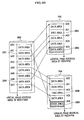
- FIG 13 is a block diagram for explaining the mapping between the virtual page address and the logical page address before the data exchange process accompanied by the wear-leveling process.
- the data area 1301 of the virtual page address area is corresponding to a data area 1303 of a logical page address area.
- the data area 1302 of the virtual page address area is corresponding to a data area 1304 of a logical page address area. For example, it is assumed that on the logical page address area, there is any free area among the data areas.
- the offset value is set to be "0"; and the free area is located before the related data area, the offset value is set to be "1".
- the offset thereof is set to be "1"; and the data area 1304 has a free area thereafter (shown in a broken line), the offset thereof is set to be "0" . Therefore, it is set that the entire memory capacity of a logical page address area becomes larger than that of a virtual page address area.
- FIG 14 is a block diagram for explaining mapping between a virtual page address and a logical page address after performing the data exchange accompanied by the wear-leveling process.
- Data area 1401 of the virtual page address area is corresponding to data area 1404 of a logical page address area; and data area 1402 of the virtual page address area is corresponding to the data area 1403 of the logical page address area.
- the offset value of the data area 1403 is "0", and the offset value of the data area 1404 is "0".
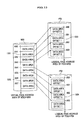
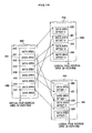
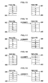
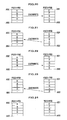
- FIG 15 to FIG 24 show how to exchange data between data area having an offset value of "0" and data area having an offset value of "1", on a step by step basis.
- a logical page address area having an offset value of "0" As shown in the drawing, the logical page address area is divided into five, as indicated in "E", “F”, “G”, “H” and “-” respectively.
- E" to "H” indicate areas on which valid data is written, and "-" indicates a free area.
- FIG 15 to FIG 24 on the right side is a logical page address area having an offset value of "1".
- the logical page address area is divided into five, as indicated in "A”, “B”, “C”, “D” and “-”, respectively.
- "A” to “D” indicate areas on which valid data is written, and "-" indicates a free area.
- FIG 15 shows an initial status before the data exchange process.
- the offset value is "0" on the left side, and the offset value is "1" on the right side.
- FIG 16 shows a status during the data exchange process, and data on the logical page address area E on the left side (the offset value of "0") is overwritten onto the free area on the right side (the offset value of "1").
- FIG 17 shows a status during the data exchange process, and data on the logical page address area A on the right side is overwritten onto the original logical page address area E on the left side.
- FIG 18 shows a status during the data exchange process, and data on the logical page address area F on the left side is overwritten onto the original logical page address area A on the right side.
- FIG 19 shows a status during the data exchange process, and data on the logical page address area B on the right side is overwritten onto the original logical page address area F on the left side.
- FIG 20 shows a status during the data exchange process, and data on the logical page address area G on the left side is overwritten onto the original logical page address area B on the right side.
- FIG 21 shows a status during the data exchange process, and data on the logical page address area C on the right side is overwritten onto the original logical page address area G on the left side.
- FIG 22 shows a status during the data exchange process, and data on the logical page address area H on the left side is overwritten onto the original logical page address area C on the right side.
- FIG 23 shows a status during the data exchange process, and data on the logical page address area D on the right side is overwritten onto the original logical page address area H on the left side.
- FIG 24 shows a final status after the data exchange process.
- the offset value is "0" on the left side, and the offset value is "0" on the right side.
- a flash memory is a semiconductor device in which an overwrite process cannot be performed on a physical address area.
- an overwrite process cannot be performed on a physical address area.
- actually data is copied onto an unused page, and then an original page on which the data is stored is set as an invalid page. Therefore, no actual overwrite process is performed onto this original page.
- the above processes are all carried out on logical page address area basis, therefore it is possible to overwrite data onto a logical page.
- the wear-leveling process can be performed based on data exchange by performing such overwrite process.
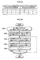
- FIG 25 is a table showing how offset values transit before/after the data exchange process.
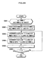
- FIG 26 is a flow chart showing the data exchange process between a logical page address area having an offset value of "0" and a logical page address area having an offset value of "1", as explained in FIG 15 to FIG 24.
- the storage controller SC herein sets a data exchange target between a logical page address area having an offset value of "0” and a logical page address area having an offset value of "1" (S2601).
- the storage controller SC moves data from the "i" th logical page address area having an offset value of "0" to the "i" th logical page address area having an offset value of "1” (S2603), and then also from the "i+1"th logical page address area having the offset value of "1” to the "i"th logical page address area having an offset value of "0” (S2604); and increases “i” by "1” (S2605).
- FIG 27 is a flow chart showing a data exchange process between a logical page address area having an offset value of "0" and a logical page address area having an offset value of "0".
- the storage controller SC herein sets a data exchange target between a logical page address area having an offset value of "0” and a logical page address area having an offset value of "0" (S2701).
- FIG 28 is a flow chart showing a data exchange process between a logical page address area having an offset value of "1" and a logical page address area having an offset value of "1".
- the storage controller SC herein sets a data exchange target between the logical page address area having the offset value of "1” and the logical page address area having the offset value of "1" (S2801).
- FIG 29 to FIG 34 are drawings for explaining a wear-leveling process according to another embodiment of the present invention.
- free areas for data exchange are distributed in a flash memory module.
- a method will be explained in which free areas are handled into a group on each module.
- FIG 29 is a block diagram for explaining mapping between a virtual page address and a logical page address before performing the data exchanging process.
- FIG 30 is a block diagram for explaining mapping between the virtual page address and the logical page address after performing the data exchanging process.
- a target wear-leveling group W00 has two flash memory modules P00, P04.
- the logical page address areas of the flash memory modules P00, P04 are provided with data area from address AC0 before address AC4.
- Area of address AC4 or more serves as free area for the data exchange (2903, 2904). This free area has the same size (data length) as that of data area for the data exchange to perform the wear-leveling process.
- FIG 31 is a table for explaining an address translation table for the data exchange between a virtual page address and a logical page address before performing the data exchange process.
- FIG 32 is a table for explaining the address translation table for the data exchange between the virtual page address and the logical page address after performing the data exchange process.
- the free areas for the data exchange are handled into a group, such a management on offset values that is required on the address translation table of FIG 10 and FIG 11 is unnecessary. Instead, it is required to manage free area locations.
- FIG 33 is a table for explaining a free area management table before performing the data exchanging process
- FIG 34 is a table for explaining the free area management table after performing the data exchange process.
- the free area management table manages a start logical page address and size (data length) of the free area in each flash memory module.
- data on the data area 2905 is written onto the free area 2904
- data on the data area 2906 is written onto the free area 2903.
- data area 3001 in the virtual page address area is set to be corresponding to data area 3004 in the logical page address area
- data area 3002 in the virtual page address area is set to be corresponding to data area 3003 in the logical page address area.
- the translation table between the virtual page address and the logical page address is updated, as shown in FIG 32.
- FIG 34 it is understood that free area for the data exchange in the flash memory module P00 is area 3005; and free area for the data exchange in the flash memory module P04 is area 3006.
- free areas for the data exchange are handled into a group per every module, instead of distributing the free area for the data exchange in a flash memory module as explained in the other embodiment, whereby a management on offset values is eliminated, resulting in an easier control on the data exchange.
- FIG 35 is a flow chart showing steps of replacing a module.
- FIG 36 to FIG 39 are block diagrams for explaining each step of the flow chart of FIG 35.
- FIG 36 shows a case when a failure occurs on a flash memory module.
- FIG 36 shows a RAID group (VDEV) V00, and wear-leveling groups (WDEV) W00, W10, W20, W30, which constitutes the RAID group VOO.
- a spare group (YDEV) Y00 is connected on a same channel D01, on which the wear-leveling group W00 is connected.
- PDEV flash memory module
- a spare group (YDEV) in which the wear-leveling (WDEV) W00 is available is selected.
- a spare group Y00 which is connected on the same channel D01 of the wear-leveling group W00 is selected (S3502).
- a flash memory module P04 is selected for the replace with the flash memory module P01 (S3503).
- FIG 37 is a block diagram for explaining a status after the flash memory module replace. As shown in FIG 37, the flash memory module P01 is replaced with the flash memory module P04 between the wear-leveling group W00 and the spare group Y00. The module P01 in failure stays on standby in replace.
- FIG 38 is a block diagram showing how to rebuild data after the flash memory replace.
- data written on the flash memory module P01 is rebuilt and written onto the flash memory module P04 which has been newly incorporated in the wear-leveling group W00 (S3504).
- W00 wear-leveling group W00
- FIG 39 is a block diagram showing a case in which a flash memory module in a spare group is replaced with a new flash memory module.
- the flash memory module P01 on standby in replace is replaced with a new flash memory module P06, and the module P06 is incorporated in the spare group Y00 (S3505). Then, the flash memory module replace is completed.
- the wear-leveling process can be performed immediately after the module replace, depending on a total write size of old module before the module replace.
- the new placed module has no total write size over the entire area of the related logical page address areas except for some writing accompanied by the data rebuilding, therefore it is impossible to know a write frequency of each predetermined area of the logical page address area.
- the total write size of the old module before the module replace can be used to learn a write frequency of the logical page address area, so that the wear-leveling process can be performed.
- aspects of the present invention provide a method of providing wear-leveling among plural flash memory modules, which is applicable to a purpose of increasing in flash memory module endurance, specifically, to a storage system using bulk flash memory with plural flash memory modules; a wear-leveling method therefor; and wear-leveling program for executing the above method.
Landscapes
- Engineering & Computer Science (AREA)
- Theoretical Computer Science (AREA)
- Physics & Mathematics (AREA)
- General Engineering & Computer Science (AREA)
- General Physics & Mathematics (AREA)
- Techniques For Improving Reliability Of Storages (AREA)
- Information Retrieval, Db Structures And Fs Structures Therefor (AREA)
- Memory System (AREA)
Priority Applications (1)
| Application Number | Priority Date | Filing Date | Title |
|---|---|---|---|
| EP11169084.8A EP2365428B1 (de) | 2006-03-29 | 2006-11-10 | Flash-Speicher verwendendes Speichersystem, abnutzungsausgleichendes Verfahren für dieses System und abnutzungsausgleichendes Programm für dieses System |
Applications Claiming Priority (1)
| Application Number | Priority Date | Filing Date | Title |
|---|---|---|---|
| JP2006092217A JP4863749B2 (ja) | 2006-03-29 | 2006-03-29 | フラッシュメモリを用いた記憶装置、その消去回数平準化方法、及び消去回数平準化プログラム |
Related Child Applications (1)
| Application Number | Title | Priority Date | Filing Date |
|---|---|---|---|
| EP11169084.8 Division-Into | 2011-06-08 |
Publications (3)
| Publication Number | Publication Date |
|---|---|
| EP1840722A2 true EP1840722A2 (de) | 2007-10-03 |
| EP1840722A3 EP1840722A3 (de) | 2009-03-04 |
| EP1840722B1 EP1840722B1 (de) | 2011-07-27 |
Family
ID=38180259
Family Applications (2)
| Application Number | Title | Priority Date | Filing Date |
|---|---|---|---|
| EP11169084.8A Not-in-force EP2365428B1 (de) | 2006-03-29 | 2006-11-10 | Flash-Speicher verwendendes Speichersystem, abnutzungsausgleichendes Verfahren für dieses System und abnutzungsausgleichendes Programm für dieses System |
| EP06255786A Not-in-force EP1840722B1 (de) | 2006-03-29 | 2006-11-10 | Flash-Speicher verwendendes Speichersystem, abnutzungsausgleichendes Verfahren für dieses System und abnutzungsausgleichendes Programm für dieses System |
Family Applications Before (1)
| Application Number | Title | Priority Date | Filing Date |
|---|---|---|---|
| EP11169084.8A Not-in-force EP2365428B1 (de) | 2006-03-29 | 2006-11-10 | Flash-Speicher verwendendes Speichersystem, abnutzungsausgleichendes Verfahren für dieses System und abnutzungsausgleichendes Programm für dieses System |
Country Status (4)
| Country | Link |
|---|---|
| US (6) | US7409492B2 (de) |
| EP (2) | EP2365428B1 (de) |
| JP (1) | JP4863749B2 (de) |
| CN (2) | CN100555244C (de) |
Cited By (20)
| Publication number | Priority date | Publication date | Assignee | Title |
|---|---|---|---|---|
| WO2010109674A1 (en) * | 2009-03-24 | 2010-09-30 | Hitachi, Ltd. | Storage apparatus and its data control method |
| EP2270672A1 (de) * | 2009-07-02 | 2011-01-05 | Giga-Byte Technology Co., Ltd. | Speicherbaustein mit Flash-Steuerung |
| WO2011021126A1 (en) * | 2009-08-21 | 2011-02-24 | International Business Machines Corporation | Data storage system and method for operating a data storage system |
| WO2011032816A1 (en) * | 2009-09-16 | 2011-03-24 | International Business Machines Corporation | Wear leveling of solid state disks based on usage information of data and parity received from a raid controller |
| GB2479235A (en) * | 2010-04-01 | 2011-10-05 | Intel Corp | Wear leveling in a solid state drive |
| US8244995B2 (en) | 2008-10-30 | 2012-08-14 | Dell Products L.P. | System and method for hierarchical wear leveling in storage devices |
| WO2013095819A1 (en) * | 2011-12-20 | 2013-06-27 | Sandisk Technologies Inc. | Wear leveling of memory devices |
| EP2413245A4 (de) * | 2009-07-22 | 2013-07-03 | Hitachi Ltd | Mit mehreren flash-kapselungen versehenes speichersystem |
| WO2013118170A1 (en) * | 2012-02-08 | 2013-08-15 | Hitachi, Ltd. | Storage apparatus with a plurality of nonvolatile semiconductor storage units and control method thereof to place hot data in storage units with higher residual life and cold data in storage units with lower residual life |
| US8639877B2 (en) | 2009-06-30 | 2014-01-28 | International Business Machines Corporation | Wear leveling of solid state disks distributed in a plurality of redundant array of independent disk ranks |
| US8694750B2 (en) | 2008-12-19 | 2014-04-08 | Nvidia Corporation | Method and system for data structure management |
| US8700839B2 (en) * | 2006-12-28 | 2014-04-15 | Genesys Logic, Inc. | Method for performing static wear leveling on flash memory |
| US9142261B2 (en) | 2011-06-30 | 2015-09-22 | Sandisk Technologies Inc. | Smart bridge for memory core |
| US9208108B2 (en) | 2008-12-19 | 2015-12-08 | Nvidia Corporation | Method and system for improved flash controller commands selection |
| US9465728B2 (en) | 2010-11-03 | 2016-10-11 | Nvidia Corporation | Memory controller adaptable to multiple memory devices |
| JP2016192213A (ja) * | 2016-05-26 | 2016-11-10 | 株式会社日立製作所 | 複数のフラッシュパッケージを有するストレージシステム |
| US9594675B2 (en) | 2009-12-31 | 2017-03-14 | Nvidia Corporation | Virtualization of chip enables |
| GB2489355B (en) * | 2009-12-30 | 2017-08-16 | Nvidia Corp | Memory device wear-leveling techniques |
| US9946471B1 (en) * | 2015-03-31 | 2018-04-17 | EMC IP Holding Company LLC | RAID groups based on endurance sets |
| EP3514674A4 (de) * | 2016-09-14 | 2020-05-06 | Alibaba Group Holding Limited | Verfahren und vorrichtung zum schreiben von gespeicherten daten in ein speichermedium basierend auf einem flash-speicher |
Families Citing this family (269)
| Publication number | Priority date | Publication date | Assignee | Title |
|---|---|---|---|---|
| JP4818812B2 (ja) * | 2006-05-31 | 2011-11-16 | 株式会社日立製作所 | フラッシュメモリストレージシステム |
| KR20050022798A (ko) * | 2003-08-30 | 2005-03-08 | 주식회사 이즈텍 | 유전자 어휘 분류체계를 이용하여 바이오 칩을 분석하기위한 시스템 및 그 방법 |
| US7590796B2 (en) * | 2006-07-31 | 2009-09-15 | Metaram, Inc. | System and method for power management in memory systems |
| US8327104B2 (en) | 2006-07-31 | 2012-12-04 | Google Inc. | Adjusting the timing of signals associated with a memory system |
| US7386656B2 (en) | 2006-07-31 | 2008-06-10 | Metaram, Inc. | Interface circuit system and method for performing power management operations in conjunction with only a portion of a memory circuit |
| US8359187B2 (en) | 2005-06-24 | 2013-01-22 | Google Inc. | Simulating a different number of memory circuit devices |
| US8244971B2 (en) | 2006-07-31 | 2012-08-14 | Google Inc. | Memory circuit system and method |
| US8130560B1 (en) | 2006-11-13 | 2012-03-06 | Google Inc. | Multi-rank partial width memory modules |
| US8438328B2 (en) | 2008-02-21 | 2013-05-07 | Google Inc. | Emulation of abstracted DIMMs using abstracted DRAMs |
| US7392338B2 (en) | 2006-07-31 | 2008-06-24 | Metaram, Inc. | Interface circuit system and method for autonomously performing power management operations in conjunction with a plurality of memory circuits |
| US8386722B1 (en) | 2008-06-23 | 2013-02-26 | Google Inc. | Stacked DIMM memory interface |
| US9542352B2 (en) | 2006-02-09 | 2017-01-10 | Google Inc. | System and method for reducing command scheduling constraints of memory circuits |
| US8055833B2 (en) * | 2006-10-05 | 2011-11-08 | Google Inc. | System and method for increasing capacity, performance, and flexibility of flash storage |
| US10013371B2 (en) | 2005-06-24 | 2018-07-03 | Google Llc | Configurable memory circuit system and method |
| US9507739B2 (en) | 2005-06-24 | 2016-11-29 | Google Inc. | Configurable memory circuit system and method |
| US7580312B2 (en) | 2006-07-31 | 2009-08-25 | Metaram, Inc. | Power saving system and method for use with a plurality of memory circuits |
| US8335894B1 (en) | 2008-07-25 | 2012-12-18 | Google Inc. | Configurable memory system with interface circuit |
| US8089795B2 (en) | 2006-02-09 | 2012-01-03 | Google Inc. | Memory module with memory stack and interface with enhanced capabilities |
| US8796830B1 (en) | 2006-09-01 | 2014-08-05 | Google Inc. | Stackable low-profile lead frame package |
| US7609567B2 (en) | 2005-06-24 | 2009-10-27 | Metaram, Inc. | System and method for simulating an aspect of a memory circuit |
| US8077535B2 (en) | 2006-07-31 | 2011-12-13 | Google Inc. | Memory refresh apparatus and method |
| US20080082763A1 (en) | 2006-10-02 | 2008-04-03 | Metaram, Inc. | Apparatus and method for power management of memory circuits by a system or component thereof |
| US8111566B1 (en) | 2007-11-16 | 2012-02-07 | Google, Inc. | Optimal channel design for memory devices for providing a high-speed memory interface |
| US8081474B1 (en) | 2007-12-18 | 2011-12-20 | Google Inc. | Embossed heat spreader |
| US8090897B2 (en) | 2006-07-31 | 2012-01-03 | Google Inc. | System and method for simulating an aspect of a memory circuit |
| US8060774B2 (en) | 2005-06-24 | 2011-11-15 | Google Inc. | Memory systems and memory modules |
| US8397013B1 (en) | 2006-10-05 | 2013-03-12 | Google Inc. | Hybrid memory module |
| US8041881B2 (en) | 2006-07-31 | 2011-10-18 | Google Inc. | Memory device with emulated characteristics |
| US9171585B2 (en) | 2005-06-24 | 2015-10-27 | Google Inc. | Configurable memory circuit system and method |
| US20080028136A1 (en) | 2006-07-31 | 2008-01-31 | Schakel Keith R | Method and apparatus for refresh management of memory modules |
| JP5242397B2 (ja) | 2005-09-02 | 2013-07-24 | メタラム インコーポレイテッド | Dramをスタックする方法及び装置 |
| US9632929B2 (en) | 2006-02-09 | 2017-04-25 | Google Inc. | Translating an address associated with a command communicated between a system and memory circuits |
| JP4842719B2 (ja) * | 2006-06-28 | 2011-12-21 | 株式会社日立製作所 | ストレージシステム及びそのデータ保護方法 |
| US7724589B2 (en) | 2006-07-31 | 2010-05-25 | Google Inc. | System and method for delaying a signal communicated from a system to at least one of a plurality of memory circuits |
| JP2008059387A (ja) * | 2006-08-31 | 2008-03-13 | Toshiba Corp | 情報処理装置、外部記憶装置および制御方法 |
| JP4372134B2 (ja) * | 2006-09-29 | 2009-11-25 | 株式会社日立製作所 | データ比較機能を有するストレージシステム |
| US7836380B2 (en) * | 2006-10-31 | 2010-11-16 | Intel Corporation | Destination indication to aid in posted write buffer loading |
| US9153337B2 (en) | 2006-12-11 | 2015-10-06 | Marvell World Trade Ltd. | Fatigue management system and method for hybrid nonvolatile solid state memory system |
| KR100881669B1 (ko) * | 2006-12-18 | 2009-02-06 | 삼성전자주식회사 | 비휘발성 데이터 저장장치의 정적 데이터 영역 검출 방법,마모도 평준화 방법 및 데이터 유닛 병합 방법과 그 장치 |
| US8140737B2 (en) * | 2007-01-30 | 2012-03-20 | Skymedi Corporation | Method for enhancing life cycle of memory |
| JP5401444B2 (ja) | 2007-03-30 | 2014-01-29 | ラムバス・インコーポレーテッド | 異なる種類の集積回路メモリ素子を有する階層メモリモジュールを含むシステム |
| US7913032B1 (en) * | 2007-04-25 | 2011-03-22 | Apple Inc. | Initiating memory wear leveling |
| TWI385666B (zh) | 2007-05-25 | 2013-02-11 | Realtek Semiconductor Corp | 適用於快閃記憶體之資料結構、及其資料寫入方法及資料讀取方法 |
| JP2009003880A (ja) * | 2007-06-25 | 2009-01-08 | Toshiba Corp | 不揮発性メモリの制御装置及びその制御方法及び記憶装置 |
| US8209479B2 (en) | 2007-07-18 | 2012-06-26 | Google Inc. | Memory circuit system and method |
| TWI372397B (en) * | 2007-08-06 | 2012-09-11 | Ind Tech Res Inst | Method and system of defect management for storage medium |
| US8080874B1 (en) | 2007-09-14 | 2011-12-20 | Google Inc. | Providing additional space between an integrated circuit and a circuit board for positioning a component therebetween |
| US8131912B2 (en) * | 2007-09-27 | 2012-03-06 | Kabushiki Kaisha Toshiba | Memory system |
| US7978516B2 (en) | 2007-12-27 | 2011-07-12 | Pliant Technology, Inc. | Flash memory controller having reduced pinout |
| JP4461170B2 (ja) * | 2007-12-28 | 2010-05-12 | 株式会社東芝 | メモリシステム |
| US7925822B2 (en) * | 2008-01-31 | 2011-04-12 | Sandisk Il Ltd | Erase count recovery |
| JP5010505B2 (ja) * | 2008-03-01 | 2012-08-29 | 株式会社東芝 | メモリシステム |
| US8074021B1 (en) | 2008-03-27 | 2011-12-06 | Netapp, Inc. | Network storage system including non-volatile solid-state memory controlled by external data layout engine |
| US7945752B1 (en) * | 2008-03-27 | 2011-05-17 | Netapp, Inc. | Method and apparatus for achieving consistent read latency from an array of solid-state storage devices |
| US8151048B1 (en) * | 2008-03-31 | 2012-04-03 | Emc Corporation | Managing storage pool provisioning |
| KR101517185B1 (ko) | 2008-04-15 | 2015-05-04 | 삼성전자주식회사 | 메모리 시스템 및 그것의 동작 방법 |
| US9501305B2 (en) * | 2008-04-23 | 2016-11-22 | Inernational Business Machines Corporation | System for virtualisation monitoring |
| US20090271564A1 (en) * | 2008-04-25 | 2009-10-29 | Hitachi, Ltd. | Storage system |
| EP2297742B1 (de) | 2008-05-16 | 2013-07-24 | Fusion-io, Inc. | Vorrichtung, system und verfahren zum detektieren und ersetzen von ausgefallenem datenspeicher |
| US8554983B2 (en) * | 2008-05-27 | 2013-10-08 | Micron Technology, Inc. | Devices and methods for operating a solid state drive |
| KR100974954B1 (ko) * | 2008-06-26 | 2010-08-10 | 에스디씨마이크로 주식회사 | 플래시 메모리를 이용한 저장장치에서의 읽기 웨어 레벨링방법 |
| JP2010015195A (ja) * | 2008-06-30 | 2010-01-21 | Toshiba Corp | 記憶制御装置及び記憶制御方法 |
| JP5242264B2 (ja) * | 2008-07-07 | 2013-07-24 | 株式会社東芝 | データ制御装置、ストレージシステムおよびプログラム |
| US20100017649A1 (en) * | 2008-07-19 | 2010-01-21 | Nanostar Corporation | Data storage system with wear-leveling algorithm |
| KR101517761B1 (ko) * | 2008-07-30 | 2015-05-06 | 시게이트 테크놀로지 엘엘씨 | 데이터 저장 위치 관리 방법 및 이를 데이터 저장 시스템 |
| CN101655776B (zh) * | 2008-08-18 | 2012-11-28 | 深圳市朗科科技股份有限公司 | 闪存卡管理系统及方法 |
| US8091362B2 (en) | 2008-08-20 | 2012-01-10 | Woodward, Inc. | Fuel injector sans support/stem |
| JP5489434B2 (ja) | 2008-08-25 | 2014-05-14 | 株式会社日立製作所 | フラッシュメモリ搭載ストレージ装置 |
| JP2010055247A (ja) * | 2008-08-27 | 2010-03-11 | Hitachi Ltd | ストレージシステム及び構成管理方法 |
| US8386697B2 (en) * | 2008-09-09 | 2013-02-26 | Phison Electronics Corp. | Memory managing method for non-volatile memory and controller using the same |
| CN101354681B (zh) * | 2008-09-23 | 2010-12-01 | 美商威睿电通公司 | 存储器系统、非易失性存储器的磨损均衡方法及装置 |
| CN101727403A (zh) * | 2008-10-15 | 2010-06-09 | 深圳市朗科科技股份有限公司 | 数据存储系统、设备及方法 |
| US8001318B1 (en) * | 2008-10-28 | 2011-08-16 | Netapp, Inc. | Wear leveling for low-wear areas of low-latency random read memory |
| US8412880B2 (en) * | 2009-01-08 | 2013-04-02 | Micron Technology, Inc. | Memory system controller to manage wear leveling across a plurality of storage nodes |
| JP4776703B2 (ja) | 2009-01-23 | 2011-09-21 | 株式会社東芝 | 半導体記憶装置を用いたraidシステム及びその制御方法 |
| JP2010198441A (ja) * | 2009-02-26 | 2010-09-09 | Toshiba Corp | ミラーリングシステム |
| US20100250826A1 (en) * | 2009-03-24 | 2010-09-30 | Micron Technology, Inc. | Memory systems with a plurality of structures and methods for operating the same |
| KR101586047B1 (ko) * | 2009-03-25 | 2016-01-18 | 삼성전자주식회사 | 불휘발성 메모리 장치 및 그것의 프로그램 방법 |
| US8661187B2 (en) | 2009-04-08 | 2014-02-25 | International Business Machines Corporation | System, method, and computer program product for skewing expected wearout times of memory devices |
| US8316173B2 (en) * | 2009-04-08 | 2012-11-20 | International Business Machines Corporation | System, method, and computer program product for analyzing monitor data information from a plurality of memory devices having finite endurance and/or retention |
| US8051241B2 (en) * | 2009-05-07 | 2011-11-01 | Seagate Technology Llc | Wear leveling technique for storage devices |
| US8307258B2 (en) | 2009-05-18 | 2012-11-06 | Fusion-10, Inc | Apparatus, system, and method for reconfiguring an array to operate with less storage elements |
| US8281227B2 (en) | 2009-05-18 | 2012-10-02 | Fusion-10, Inc. | Apparatus, system, and method to increase data integrity in a redundant storage system |
| WO2010134300A1 (ja) * | 2009-05-21 | 2010-11-25 | パナソニック株式会社 | メモリコントローラ、不揮発性記憶装置、アクセス装置、不揮発性記憶システム、データ書き込み方法、および、プログラム |
| US8375162B2 (en) * | 2009-06-03 | 2013-02-12 | Ocz Technology Group Inc. | Method and apparatus for reducing write cycles in NAND-based flash memory devices |
| WO2010144624A1 (en) | 2009-06-09 | 2010-12-16 | Google Inc. | Programming of dimm termination resistance values |
| US8447915B2 (en) * | 2009-07-23 | 2013-05-21 | Hitachi, Ltd. | Flash memory device for allocating physical blocks to logical blocks based on an erase count |
| US7941696B2 (en) * | 2009-08-11 | 2011-05-10 | Texas Memory Systems, Inc. | Flash-based memory system with static or variable length page stripes including data protection information and auxiliary protection stripes |
| US7856528B1 (en) * | 2009-08-11 | 2010-12-21 | Texas Memory Systems, Inc. | Method and apparatus for protecting data using variable size page stripes in a FLASH-based storage system |
| US8495423B2 (en) * | 2009-08-11 | 2013-07-23 | International Business Machines Corporation | Flash-based memory system with robust backup and restart features and removable modules |
| US8930622B2 (en) | 2009-08-11 | 2015-01-06 | International Business Machines Corporation | Multi-level data protection for flash memory system |
| US7818525B1 (en) | 2009-08-12 | 2010-10-19 | Texas Memory Systems, Inc. | Efficient reduction of read disturb errors in NAND FLASH memory |
| US8189379B2 (en) | 2009-08-12 | 2012-05-29 | Texas Memory Systems, Inc. | Reduction of read disturb errors in NAND FLASH memory |
| US20110047316A1 (en) * | 2009-08-19 | 2011-02-24 | Dell Products L.P. | Solid state memory device power optimization |
| WO2011021237A1 (en) * | 2009-08-20 | 2011-02-24 | Hitachi,Ltd. | Storage subsystem and its data processing method |
| US8464106B2 (en) * | 2009-08-24 | 2013-06-11 | Ocz Technology Group, Inc. | Computer system with backup function and method therefor |
| US8266501B2 (en) * | 2009-09-29 | 2012-09-11 | Micron Technology, Inc. | Stripe based memory operation |
| JP5336993B2 (ja) * | 2009-10-14 | 2013-11-06 | 株式会社日立国際電気 | 映像記録装置及び映像記録方法 |
| JP5525605B2 (ja) * | 2009-11-04 | 2014-06-18 | 株式会社日立製作所 | フラッシュメモリモジュール |
| TWI436369B (zh) | 2009-11-13 | 2014-05-01 | Silicon Motion Inc | 記憶裝置之使用壽命量測方法及系統內編程碼置換方法、及其資料儲存系統 |
| JP4912456B2 (ja) * | 2009-12-17 | 2012-04-11 | 株式会社日立製作所 | ストレージ装置及びその制御方法 |
| JP5331018B2 (ja) * | 2010-01-22 | 2013-10-30 | 株式会社日立製作所 | ソリッド・ステート・ドライブ装置およびミラー構成再構成方法 |
| US20110215007A1 (en) * | 2010-02-19 | 2011-09-08 | Kenneth Charles Wurtzel | Container or molded package with buffering capacity |
| US8365041B2 (en) | 2010-03-17 | 2013-01-29 | Sandisk Enterprise Ip Llc | MLC self-raid flash data protection scheme |
| JP5385835B2 (ja) * | 2010-03-29 | 2014-01-08 | パナソニック株式会社 | データ記録装置 |
| JP5646633B2 (ja) * | 2010-04-12 | 2014-12-24 | 株式会社日立製作所 | ストレージ装置 |
| US8700841B2 (en) * | 2010-04-19 | 2014-04-15 | International Business Machines Corporation | Sub-LUN input/output profiling for SSD devices |
| JP5100789B2 (ja) * | 2010-05-28 | 2012-12-19 | 株式会社東芝 | 半導体記憶装置および半導体記憶装置の制御方法 |
| JP5521794B2 (ja) * | 2010-06-03 | 2014-06-18 | 株式会社バッファロー | 記憶装置及びその制御プログラム |
| CN102280126B (zh) * | 2010-06-13 | 2015-11-25 | 宇瞻科技股份有限公司 | 可扩充存储器单元的存储装置 |
| KR20110138707A (ko) * | 2010-06-21 | 2011-12-28 | 삼성전자주식회사 | 데이터 저장 장치 및 그것의 쓰기 방법 |
| US9141538B2 (en) | 2010-07-07 | 2015-09-22 | Marvell World Trade Ltd. | Apparatus and method for generating descriptors to transfer data to and from non-volatile semiconductor memory of a storage drive |
| US8868852B2 (en) * | 2010-07-07 | 2014-10-21 | Marvell World Trade Ltd. | Interface management control systems and methods for non-volatile semiconductor memory |
| US9135168B2 (en) | 2010-07-07 | 2015-09-15 | Marvell World Trade Ltd. | Apparatus and method for generating descriptors to reaccess a non-volatile semiconductor memory of a storage drive due to an error |
| JP5641900B2 (ja) * | 2010-11-29 | 2014-12-17 | キヤノン株式会社 | 管理装置及びその制御方法、並びにプログラム |
| US8601313B1 (en) * | 2010-12-13 | 2013-12-03 | Western Digital Technologies, Inc. | System and method for a data reliability scheme in a solid state memory |
| US8615681B2 (en) * | 2010-12-14 | 2013-12-24 | Western Digital Technologies, Inc. | System and method for maintaining a data redundancy scheme in a solid state memory in the event of a power loss |
| US8601311B2 (en) | 2010-12-14 | 2013-12-03 | Western Digital Technologies, Inc. | System and method for using over-provisioned data capacity to maintain a data redundancy scheme in a solid state memory |
| KR101180406B1 (ko) * | 2011-01-28 | 2012-09-10 | 에스케이하이닉스 주식회사 | 비휘발성 메모리 시스템 및 블럭 관리 방법 |
| US8966184B2 (en) | 2011-01-31 | 2015-02-24 | Intelligent Intellectual Property Holdings 2, LLC. | Apparatus, system, and method for managing eviction of data |
| US8700950B1 (en) | 2011-02-11 | 2014-04-15 | Western Digital Technologies, Inc. | System and method for data error recovery in a solid state subsystem |
| JP5664347B2 (ja) * | 2011-03-04 | 2015-02-04 | ソニー株式会社 | 仮想メモリシステム、仮想メモリの制御方法、およびプログラム |
| US8621328B2 (en) * | 2011-03-04 | 2013-12-31 | International Business Machines Corporation | Wear-focusing of non-volatile memories for improved endurance |
| US8700951B1 (en) | 2011-03-09 | 2014-04-15 | Western Digital Technologies, Inc. | System and method for improving a data redundancy scheme in a solid state subsystem with additional metadata |
| US8862804B2 (en) | 2011-04-29 | 2014-10-14 | Western Digital Technologies, Inc. | System and method for improved parity determination within a data redundancy scheme in a solid state memory |
| KR20120128978A (ko) * | 2011-05-18 | 2012-11-28 | 삼성전자주식회사 | 데이터 저장 장치 및 그것의 데이터 관리 방법 |
| US8909982B2 (en) | 2011-06-19 | 2014-12-09 | Sandisk Enterprise Ip Llc | System and method for detecting copyback programming problems |
| US8910020B2 (en) | 2011-06-19 | 2014-12-09 | Sandisk Enterprise Ip Llc | Intelligent bit recovery for flash memory |
| US8626991B1 (en) * | 2011-06-30 | 2014-01-07 | Emc Corporation | Multi-LUN SSD optimization system and method |
| CN103946819B (zh) | 2011-09-30 | 2017-05-17 | 英特尔公司 | 用于非易失性系统存储器的统计耗损均衡 |
| CN102439572B (zh) * | 2011-10-27 | 2014-04-02 | 华为技术有限公司 | 控制缓存映射的方法及缓存系统 |
| US9058289B2 (en) | 2011-11-07 | 2015-06-16 | Sandisk Enterprise Ip Llc | Soft information generation for memory systems |
| US8924815B2 (en) | 2011-11-18 | 2014-12-30 | Sandisk Enterprise Ip Llc | Systems, methods and devices for decoding codewords having multiple parity segments |
| US9048876B2 (en) | 2011-11-18 | 2015-06-02 | Sandisk Enterprise Ip Llc | Systems, methods and devices for multi-tiered error correction |
| US8954822B2 (en) | 2011-11-18 | 2015-02-10 | Sandisk Enterprise Ip Llc | Data encoder and decoder using memory-specific parity-check matrix |
| US9767032B2 (en) | 2012-01-12 | 2017-09-19 | Sandisk Technologies Llc | Systems and methods for cache endurance |
| CN102662695B (zh) * | 2012-03-26 | 2016-03-30 | 华为终端有限公司 | 一种系统启动的方法及装置 |
| TWI495998B (zh) * | 2012-08-01 | 2015-08-11 | Phison Electronics Corp | 資料管理方法、記憶體控制器與記憶體儲存裝置 |
| US20140052897A1 (en) * | 2012-08-17 | 2014-02-20 | Seagate Technology Llc | Dynamic formation of garbage collection units in a memory |
| US9699263B1 (en) | 2012-08-17 | 2017-07-04 | Sandisk Technologies Llc. | Automatic read and write acceleration of data accessed by virtual machines |
| JP5820078B2 (ja) * | 2012-09-07 | 2015-11-24 | 株式会社日立製作所 | 記憶装置システム |
| US9013922B2 (en) * | 2012-09-20 | 2015-04-21 | Silicon Motion, Inc. | Data storage device and flash memory control method thereof |
| JP5949408B2 (ja) * | 2012-10-02 | 2016-07-06 | 富士通株式会社 | 情報処理装置、情報処理装置の制御方法および情報処理装置の制御プログラム |
| US8972826B2 (en) | 2012-10-24 | 2015-03-03 | Western Digital Technologies, Inc. | Adaptive error correction codes for data storage systems |
| JP2014098978A (ja) | 2012-11-13 | 2014-05-29 | Sony Corp | メモリ制御装置、メモリシステム、情報処理システムおよびメモリ制御方法 |
| US9021339B2 (en) | 2012-11-29 | 2015-04-28 | Western Digital Technologies, Inc. | Data reliability schemes for data storage systems |
| US9059736B2 (en) | 2012-12-03 | 2015-06-16 | Western Digital Technologies, Inc. | Methods, solid state drive controllers and data storage devices having a runtime variable raid protection scheme |
| CN103049216B (zh) * | 2012-12-07 | 2015-11-25 | 记忆科技(深圳)有限公司 | 固态硬盘及其数据处理方法、系统 |
| US9214963B1 (en) | 2012-12-21 | 2015-12-15 | Western Digital Technologies, Inc. | Method and system for monitoring data channel to enable use of dynamically adjustable LDPC coding parameters in a data storage system |
| US9501398B2 (en) | 2012-12-26 | 2016-11-22 | Sandisk Technologies Llc | Persistent storage device with NVRAM for staging writes |
| US9612948B2 (en) | 2012-12-27 | 2017-04-04 | Sandisk Technologies Llc | Reads and writes between a contiguous data block and noncontiguous sets of logical address blocks in a persistent storage device |
| US9239751B1 (en) | 2012-12-27 | 2016-01-19 | Sandisk Enterprise Ip Llc | Compressing data from multiple reads for error control management in memory systems |
| US9003264B1 (en) | 2012-12-31 | 2015-04-07 | Sandisk Enterprise Ip Llc | Systems, methods, and devices for multi-dimensional flash RAID data protection |
| US9454420B1 (en) | 2012-12-31 | 2016-09-27 | Sandisk Technologies Llc | Method and system of reading threshold voltage equalization |
| US10445229B1 (en) | 2013-01-28 | 2019-10-15 | Radian Memory Systems, Inc. | Memory controller with at least one address segment defined for which data is striped across flash memory dies, with a common address offset being used to obtain physical addresses for the data in each of the dies |
| US9652376B2 (en) | 2013-01-28 | 2017-05-16 | Radian Memory Systems, Inc. | Cooperative flash memory control |
| US11249652B1 (en) | 2013-01-28 | 2022-02-15 | Radian Memory Systems, Inc. | Maintenance of nonvolatile memory on host selected namespaces by a common memory controller |
| US9214965B2 (en) | 2013-02-20 | 2015-12-15 | Sandisk Enterprise Ip Llc | Method and system for improving data integrity in non-volatile storage |
| US9329928B2 (en) | 2013-02-20 | 2016-05-03 | Sandisk Enterprise IP LLC. | Bandwidth optimization in a non-volatile memory system |
| US9383924B1 (en) * | 2013-02-27 | 2016-07-05 | Netapp, Inc. | Storage space reclamation on volumes with thin provisioning capability |
| US8943266B2 (en) | 2013-03-13 | 2015-01-27 | Hitachi, Ltd. | Storage system and method of control for storage system |
| US9870830B1 (en) | 2013-03-14 | 2018-01-16 | Sandisk Technologies Llc | Optimal multilevel sensing for reading data from a storage medium |
| US9092350B1 (en) | 2013-03-15 | 2015-07-28 | Sandisk Enterprise Ip Llc | Detection and handling of unbalanced errors in interleaved codewords |
| US9009576B1 (en) | 2013-03-15 | 2015-04-14 | Sandisk Enterprise Ip Llc | Adaptive LLR based on syndrome weight |
| US9136877B1 (en) | 2013-03-15 | 2015-09-15 | Sandisk Enterprise Ip Llc | Syndrome layered decoding for LDPC codes |
| US9236886B1 (en) | 2013-03-15 | 2016-01-12 | Sandisk Enterprise Ip Llc | Universal and reconfigurable QC-LDPC encoder |
| US9244763B1 (en) | 2013-03-15 | 2016-01-26 | Sandisk Enterprise Ip Llc | System and method for updating a reading threshold voltage based on symbol transition information |
| US9367246B2 (en) | 2013-03-15 | 2016-06-14 | Sandisk Technologies Inc. | Performance optimization of data transfer for soft information generation |
| TWI570738B (zh) * | 2013-03-29 | 2017-02-11 | 萬國商業機器公司 | 具有使用歷程記錄的主記憶體模組以及此主記憶體模組於電腦系統之應用 |
| US10049037B2 (en) | 2013-04-05 | 2018-08-14 | Sandisk Enterprise Ip Llc | Data management in a storage system |
| US9170941B2 (en) | 2013-04-05 | 2015-10-27 | Sandisk Enterprises IP LLC | Data hardening in a storage system |
| US9946495B2 (en) | 2013-04-25 | 2018-04-17 | Microsoft Technology Licensing, Llc | Dirty data management for hybrid drives |
| US9159437B2 (en) | 2013-06-11 | 2015-10-13 | Sandisk Enterprise IP LLC. | Device and method for resolving an LM flag issue |
| CN103688248B (zh) * | 2013-06-29 | 2015-09-30 | 华为技术有限公司 | 一种存储阵列的管理方法、装置和控制器 |
| WO2015008375A1 (ja) | 2013-07-19 | 2015-01-22 | 株式会社日立製作所 | ストレージ装置および記憶制御方法 |
| US9384126B1 (en) | 2013-07-25 | 2016-07-05 | Sandisk Technologies Inc. | Methods and systems to avoid false negative results in bloom filters implemented in non-volatile data storage systems |
| US9524235B1 (en) | 2013-07-25 | 2016-12-20 | Sandisk Technologies Llc | Local hash value generation in non-volatile data storage systems |
| US9043517B1 (en) | 2013-07-25 | 2015-05-26 | Sandisk Enterprise Ip Llc | Multipass programming in buffers implemented in non-volatile data storage systems |
| US9361221B1 (en) | 2013-08-26 | 2016-06-07 | Sandisk Technologies Inc. | Write amplification reduction through reliable writes during garbage collection |
| US9639463B1 (en) | 2013-08-26 | 2017-05-02 | Sandisk Technologies Llc | Heuristic aware garbage collection scheme in storage systems |
| US9442670B2 (en) | 2013-09-03 | 2016-09-13 | Sandisk Technologies Llc | Method and system for rebalancing data stored in flash memory devices |
| US9519577B2 (en) | 2013-09-03 | 2016-12-13 | Sandisk Technologies Llc | Method and system for migrating data between flash memory devices |
| US9158349B2 (en) | 2013-10-04 | 2015-10-13 | Sandisk Enterprise Ip Llc | System and method for heat dissipation |
| US9323637B2 (en) | 2013-10-07 | 2016-04-26 | Sandisk Enterprise Ip Llc | Power sequencing and data hardening architecture |
| US9298608B2 (en) | 2013-10-18 | 2016-03-29 | Sandisk Enterprise Ip Llc | Biasing for wear leveling in storage systems |
| US10019352B2 (en) | 2013-10-18 | 2018-07-10 | Sandisk Technologies Llc | Systems and methods for adaptive reserve storage |
| US9442662B2 (en) | 2013-10-18 | 2016-09-13 | Sandisk Technologies Llc | Device and method for managing die groups |
| US9436831B2 (en) | 2013-10-30 | 2016-09-06 | Sandisk Technologies Llc | Secure erase in a memory device |
| US9263156B2 (en) | 2013-11-07 | 2016-02-16 | Sandisk Enterprise Ip Llc | System and method for adjusting trip points within a storage device |
| JP5673980B2 (ja) * | 2013-11-13 | 2015-02-18 | 国立大学法人 千葉大学 | 記録装置 |
| US9244785B2 (en) | 2013-11-13 | 2016-01-26 | Sandisk Enterprise Ip Llc | Simulated power failure and data hardening |
| US9229640B2 (en) | 2013-11-15 | 2016-01-05 | Microsoft Technology Licensing, Llc | Inexpensive solid-state storage by throttling write speed in accordance with empirically derived write policy table |
| US9152555B2 (en) | 2013-11-15 | 2015-10-06 | Sandisk Enterprise IP LLC. | Data management with modular erase in a data storage system |
| US9703816B2 (en) | 2013-11-19 | 2017-07-11 | Sandisk Technologies Llc | Method and system for forward reference logging in a persistent datastore |
| US9612773B2 (en) * | 2013-11-21 | 2017-04-04 | Samsung Electronics Co., Ltd. | User device having a host flash translation layer (FTL), a method for transferring an erase count thereof, a method for transferring reprogram information thereof, and a method for transferring a page offset of an open block thereof |
| US9520197B2 (en) | 2013-11-22 | 2016-12-13 | Sandisk Technologies Llc | Adaptive erase of a storage device |
| US9122636B2 (en) | 2013-11-27 | 2015-09-01 | Sandisk Enterprise Ip Llc | Hard power fail architecture |
| US9520162B2 (en) | 2013-11-27 | 2016-12-13 | Sandisk Technologies Llc | DIMM device controller supervisor |
| US9280429B2 (en) | 2013-11-27 | 2016-03-08 | Sandisk Enterprise Ip Llc | Power fail latching based on monitoring multiple power supply voltages in a storage device |
| US9250676B2 (en) | 2013-11-29 | 2016-02-02 | Sandisk Enterprise Ip Llc | Power failure architecture and verification |
| US9582058B2 (en) | 2013-11-29 | 2017-02-28 | Sandisk Technologies Llc | Power inrush management of storage devices |
| US9092370B2 (en) | 2013-12-03 | 2015-07-28 | Sandisk Enterprise Ip Llc | Power failure tolerant cryptographic erase |
| US9235245B2 (en) | 2013-12-04 | 2016-01-12 | Sandisk Enterprise Ip Llc | Startup performance and power isolation |
| JP5768118B2 (ja) * | 2013-12-11 | 2015-08-26 | 株式会社日立製作所 | 複数のフラッシュパッケージを有するストレージシステム |
| WO2015087651A1 (ja) * | 2013-12-12 | 2015-06-18 | 株式会社フィックスターズ | メモリの使用可能期間を延ばすための装置、プログラム、記録媒体および方法 |
| US9129665B2 (en) | 2013-12-17 | 2015-09-08 | Sandisk Enterprise Ip Llc | Dynamic brownout adjustment in a storage device |
| US9549457B2 (en) | 2014-02-12 | 2017-01-17 | Sandisk Technologies Llc | System and method for redirecting airflow across an electronic assembly |
| US9497889B2 (en) | 2014-02-27 | 2016-11-15 | Sandisk Technologies Llc | Heat dissipation for substrate assemblies |
| US9703636B2 (en) | 2014-03-01 | 2017-07-11 | Sandisk Technologies Llc | Firmware reversion trigger and control |
| US9485851B2 (en) | 2014-03-14 | 2016-11-01 | Sandisk Technologies Llc | Thermal tube assembly structures |
| US9519319B2 (en) | 2014-03-14 | 2016-12-13 | Sandisk Technologies Llc | Self-supporting thermal tube structure for electronic assemblies |
| US9348377B2 (en) | 2014-03-14 | 2016-05-24 | Sandisk Enterprise Ip Llc | Thermal isolation techniques |
| US9390814B2 (en) | 2014-03-19 | 2016-07-12 | Sandisk Technologies Llc | Fault detection and prediction for data storage elements |
| US9448876B2 (en) | 2014-03-19 | 2016-09-20 | Sandisk Technologies Llc | Fault detection and prediction in storage devices |
| US9454448B2 (en) | 2014-03-19 | 2016-09-27 | Sandisk Technologies Llc | Fault testing in storage devices |
| US9390021B2 (en) | 2014-03-31 | 2016-07-12 | Sandisk Technologies Llc | Efficient cache utilization in a tiered data structure |
| US9626400B2 (en) | 2014-03-31 | 2017-04-18 | Sandisk Technologies Llc | Compaction of information in tiered data structure |
| US9626399B2 (en) | 2014-03-31 | 2017-04-18 | Sandisk Technologies Llc | Conditional updates for reducing frequency of data modification operations |
| US9697267B2 (en) | 2014-04-03 | 2017-07-04 | Sandisk Technologies Llc | Methods and systems for performing efficient snapshots in tiered data structures |
| US9471428B2 (en) | 2014-05-06 | 2016-10-18 | International Business Machines Corporation | Using spare capacity in solid state drives |
| US9703491B2 (en) | 2014-05-30 | 2017-07-11 | Sandisk Technologies Llc | Using history of unaligned writes to cache data and avoid read-modify-writes in a non-volatile storage device |
| US10372613B2 (en) | 2014-05-30 | 2019-08-06 | Sandisk Technologies Llc | Using sub-region I/O history to cache repeatedly accessed sub-regions in a non-volatile storage device |
| US9093160B1 (en) | 2014-05-30 | 2015-07-28 | Sandisk Technologies Inc. | Methods and systems for staggered memory operations |
| US9645749B2 (en) | 2014-05-30 | 2017-05-09 | Sandisk Technologies Llc | Method and system for recharacterizing the storage density of a memory device or a portion thereof |
| US10146448B2 (en) | 2014-05-30 | 2018-12-04 | Sandisk Technologies Llc | Using history of I/O sequences to trigger cached read ahead in a non-volatile storage device |
| US10162748B2 (en) | 2014-05-30 | 2018-12-25 | Sandisk Technologies Llc | Prioritizing garbage collection and block allocation based on I/O history for logical address regions |
| US9070481B1 (en) | 2014-05-30 | 2015-06-30 | Sandisk Technologies Inc. | Internal current measurement for age measurements |
| US8891303B1 (en) | 2014-05-30 | 2014-11-18 | Sandisk Technologies Inc. | Method and system for dynamic word line based configuration of a three-dimensional memory device |
| US10656840B2 (en) | 2014-05-30 | 2020-05-19 | Sandisk Technologies Llc | Real-time I/O pattern recognition to enhance performance and endurance of a storage device |
| US10114557B2 (en) | 2014-05-30 | 2018-10-30 | Sandisk Technologies Llc | Identification of hot regions to enhance performance and endurance of a non-volatile storage device |
| US10656842B2 (en) | 2014-05-30 | 2020-05-19 | Sandisk Technologies Llc | Using history of I/O sizes and I/O sequences to trigger coalesced writes in a non-volatile storage device |
| US9471451B2 (en) | 2014-06-18 | 2016-10-18 | International Business Machines Corporation | Implementing enhanced wear leveling in 3D flash memories |
| US9652381B2 (en) | 2014-06-19 | 2017-05-16 | Sandisk Technologies Llc | Sub-block garbage collection |
| JP6331773B2 (ja) | 2014-06-30 | 2018-05-30 | 富士通株式会社 | ストレージ制御装置、およびストレージ制御プログラム |
| US9443601B2 (en) | 2014-09-08 | 2016-09-13 | Sandisk Technologies Llc | Holdup capacitor energy harvesting |
| US9542118B1 (en) | 2014-09-09 | 2017-01-10 | Radian Memory Systems, Inc. | Expositive flash memory control |
| US10552085B1 (en) | 2014-09-09 | 2020-02-04 | Radian Memory Systems, Inc. | Techniques for directed data migration |
| US10127157B2 (en) * | 2014-10-06 | 2018-11-13 | SK Hynix Inc. | Sizing a cache while taking into account a total bytes written requirement |
| TWI539282B (zh) * | 2014-10-13 | 2016-06-21 | 慧榮科技股份有限公司 | 非揮發性儲存裝置與控制器 |
| KR102211868B1 (ko) * | 2014-12-15 | 2021-02-04 | 삼성전자주식회사 | 스토리지 장치 및 스토리지 장치의 동작 방법 |
| US11042300B2 (en) | 2015-03-31 | 2021-06-22 | Toshiba Memory Corporation | Command load balancing for NVME dual port operations |
| JP5945040B2 (ja) * | 2015-06-19 | 2016-07-05 | 株式会社日立製作所 | 複数のフラッシュパッケージを有するストレージシステム |
| US10552058B1 (en) | 2015-07-17 | 2020-02-04 | Radian Memory Systems, Inc. | Techniques for delegating data processing to a cooperative memory controller |
| CN105260320B (zh) * | 2015-10-12 | 2020-06-16 | 珠海格力电器股份有限公司 | 用于flash存储器的数据处理方法和装置 |
| TWI547801B (zh) * | 2015-10-22 | 2016-09-01 | Accelstor Inc | 資料儲存系統及方法 |
| CN105353977B (zh) * | 2015-10-22 | 2018-11-23 | 捷鼎创新股份有限公司 | 数据储存系统及方法 |
| US10146465B1 (en) * | 2015-12-18 | 2018-12-04 | EMC IP Holding Company LLC | Automated provisioning and de-provisioning software defined storage systems |
| US10222984B1 (en) * | 2015-12-31 | 2019-03-05 | EMC IP Holding Company LLC | Managing multi-granularity flash translation layers in solid state drives |
| TWI591635B (zh) * | 2016-02-05 | 2017-07-11 | 群聯電子股份有限公司 | 記憶體管理方法、記憶體控制電路單元與記憶體儲存裝置 |
| US9959058B1 (en) | 2016-03-31 | 2018-05-01 | EMC IP Holding Company LLC | Utilizing flash optimized layouts which minimize wear of internal flash memory of solid state drives |
| CN108205423B (zh) * | 2016-12-20 | 2020-06-02 | 华为技术有限公司 | 一种物理硬盘磨损均衡方法、装置及系统 |
| WO2018124912A1 (en) | 2016-12-28 | 2018-07-05 | EMC IP Holding Company LLC | Data storage system tiering accounting for limited write endurance |
| US10860733B1 (en) * | 2017-04-20 | 2020-12-08 | EMC IP Holding Company, LLC | Shredding system and method |
| CN108563397B (zh) * | 2018-01-04 | 2021-08-24 | 威盛电子股份有限公司 | 存储装置以及数据保存方法 |
| CN108089994B (zh) * | 2018-01-04 | 2021-06-01 | 威盛电子股份有限公司 | 存储装置以及数据保存方法 |
| US10782908B2 (en) | 2018-02-05 | 2020-09-22 | Micron Technology, Inc. | Predictive data orchestration in multi-tier memory systems |
| US12135876B2 (en) | 2018-02-05 | 2024-11-05 | Micron Technology, Inc. | Memory systems having controllers embedded in packages of integrated circuit memory |
| US11099789B2 (en) | 2018-02-05 | 2021-08-24 | Micron Technology, Inc. | Remote direct memory access in multi-tier memory systems |
| US11416395B2 (en) | 2018-02-05 | 2022-08-16 | Micron Technology, Inc. | Memory virtualization for accessing heterogeneous memory components |
| US10884889B2 (en) | 2018-06-22 | 2021-01-05 | Seagate Technology Llc | Allocating part of a raid stripe to repair a second raid stripe |
| KR102545189B1 (ko) | 2018-09-07 | 2023-06-19 | 삼성전자주식회사 | 스토리지 장치, 스토리지 시스템 및 스토리지 장치의 동작 방법 |
| KR102663661B1 (ko) * | 2018-12-06 | 2024-05-10 | 에스케이하이닉스 주식회사 | 메모리 시스템 내 저장된 데이터를 제어하는 방법 및 장치 |
| KR102816405B1 (ko) * | 2019-01-07 | 2025-06-04 | 에스케이하이닉스 주식회사 | 데이터 저장 장치 및 동작 방법, 이를 위한 컨트롤러 |
| US10852949B2 (en) | 2019-04-15 | 2020-12-01 | Micron Technology, Inc. | Predictive data pre-fetching in a data storage device |
| CN112764665B (zh) * | 2019-10-21 | 2024-05-10 | 伊姆西Ip控股有限责任公司 | 存储管理的方法、设备和计算机程序产品 |
| US11175984B1 (en) | 2019-12-09 | 2021-11-16 | Radian Memory Systems, Inc. | Erasure coding techniques for flash memory |
| US11442631B2 (en) * | 2019-12-26 | 2022-09-13 | Micron Technology, Inc. | Memory operations with consideration for wear leveling |
| US11586385B1 (en) | 2020-05-06 | 2023-02-21 | Radian Memory Systems, Inc. | Techniques for managing writes in nonvolatile memory |
| CN115620789A (zh) * | 2022-09-29 | 2023-01-17 | 武汉新芯集成电路制造有限公司 | 存储芯片 |
Family Cites Families (22)
| Publication number | Priority date | Publication date | Assignee | Title |
|---|---|---|---|---|
| US3581132A (en) * | 1969-04-03 | 1971-05-25 | Nikolaus Laing | Rotating electrical machine |
| US6230233B1 (en) * | 1991-09-13 | 2001-05-08 | Sandisk Corporation | Wear leveling techniques for flash EEPROM systems |
| JP3507132B2 (ja) * | 1994-06-29 | 2004-03-15 | 株式会社日立製作所 | フラッシュメモリを用いた記憶装置およびその記憶制御方法 |
| DE19540915A1 (de) * | 1994-11-10 | 1996-05-15 | Raymond Engineering | Redundante Anordnung von Festkörper-Speicherbausteinen |
| JPH09218754A (ja) * | 1996-02-13 | 1997-08-19 | Ekushingu:Kk | データ記憶システム |
| WO1999031592A1 (fr) * | 1997-12-16 | 1999-06-24 | Tdk Corporation | Systeme de memoire flash |
| JP2000207137A (ja) * | 1999-01-12 | 2000-07-28 | Kowa Co | 情報記憶装置 |
| US7457897B1 (en) * | 2004-03-17 | 2008-11-25 | Suoer Talent Electronics, Inc. | PCI express-compatible controller and interface for flash memory |
| US7934074B2 (en) * | 1999-08-04 | 2011-04-26 | Super Talent Electronics | Flash module with plane-interleaved sequential writes to restricted-write flash chips |
| US7966462B2 (en) * | 1999-08-04 | 2011-06-21 | Super Talent Electronics, Inc. | Multi-channel flash module with plane-interleaved sequential ECC writes and background recycling to restricted-write flash chips |
| US8037234B2 (en) * | 2003-12-02 | 2011-10-11 | Super Talent Electronics, Inc. | Command queuing smart storage transfer manager for striping data to raw-NAND flash modules |
| US8341332B2 (en) * | 2003-12-02 | 2012-12-25 | Super Talent Electronics, Inc. | Multi-level controller with smart storage transfer manager for interleaving multiple single-chip flash memory devices |
| US8266367B2 (en) * | 2003-12-02 | 2012-09-11 | Super Talent Electronics, Inc. | Multi-level striping and truncation channel-equalization for flash-memory system |
| JP2001318829A (ja) * | 2000-05-08 | 2001-11-16 | Funai Electric Co Ltd | フラッシュメモリの書換制御装置、及び、フラッシュメモリの書換制御方法 |
| JP2004021811A (ja) * | 2002-06-19 | 2004-01-22 | Hitachi Ltd | 不揮発メモリを使用したディスク制御装置 |
| US6941412B2 (en) | 2002-08-29 | 2005-09-06 | Sandisk Corporation | Symbol frequency leveling in a storage system |
| KR101122511B1 (ko) * | 2002-10-28 | 2012-03-15 | 쌘디스크 코포레이션 | 비휘발성 저장 시스템들에서 자동 웨어 레벨링 |
| US20090204872A1 (en) * | 2003-12-02 | 2009-08-13 | Super Talent Electronics Inc. | Command Queuing Smart Storage Transfer Manager for Striping Data to Raw-NAND Flash Modules |
| US8176238B2 (en) * | 2003-12-02 | 2012-05-08 | Super Talent Electronics, Inc. | Command queuing smart storage transfer manager for striping data to raw-NAND flash modules |
| US7395404B2 (en) * | 2004-12-16 | 2008-07-01 | Sandisk Corporation | Cluster auto-alignment for storing addressable data packets in a non-volatile memory array |
| US7315917B2 (en) * | 2005-01-20 | 2008-01-01 | Sandisk Corporation | Scheduling of housekeeping operations in flash memory systems |
| US20060161724A1 (en) * | 2005-01-20 | 2006-07-20 | Bennett Alan D | Scheduling of housekeeping operations in flash memory systems |
-
2006
- 2006-03-29 JP JP2006092217A patent/JP4863749B2/ja not_active Expired - Lifetime
- 2006-05-26 US US11/441,192 patent/US7409492B2/en not_active Expired - Fee Related
- 2006-11-10 EP EP11169084.8A patent/EP2365428B1/de not_active Not-in-force
- 2006-11-10 EP EP06255786A patent/EP1840722B1/de not_active Not-in-force
- 2006-12-19 CN CNB2006101687026A patent/CN100555244C/zh not_active Expired - Fee Related
- 2006-12-19 CN CN2009101731304A patent/CN101645041B/zh not_active Expired - Fee Related
-
2008
- 2008-07-02 US US12/216,362 patent/US7734865B2/en not_active Expired - Fee Related
-
2010
- 2010-04-22 US US12/765,594 patent/US7970986B2/en not_active Expired - Fee Related
-
2011
- 2011-06-01 US US13/151,015 patent/US8429340B2/en not_active Expired - Fee Related
-
2013
- 2013-03-26 US US13/850,972 patent/US8788745B2/en active Active
-
2014
- 2014-07-08 US US14/325,469 patent/US9286210B2/en active Active
Non-Patent Citations (1)
| Title |
|---|
| None |
Cited By (43)
| Publication number | Priority date | Publication date | Assignee | Title |
|---|---|---|---|---|
| US8700839B2 (en) * | 2006-12-28 | 2014-04-15 | Genesys Logic, Inc. | Method for performing static wear leveling on flash memory |
| US8244995B2 (en) | 2008-10-30 | 2012-08-14 | Dell Products L.P. | System and method for hierarchical wear leveling in storage devices |
| US9208108B2 (en) | 2008-12-19 | 2015-12-08 | Nvidia Corporation | Method and system for improved flash controller commands selection |
| US8694750B2 (en) | 2008-12-19 | 2014-04-08 | Nvidia Corporation | Method and system for data structure management |
| WO2010109674A1 (en) * | 2009-03-24 | 2010-09-30 | Hitachi, Ltd. | Storage apparatus and its data control method |
| US8639877B2 (en) | 2009-06-30 | 2014-01-28 | International Business Machines Corporation | Wear leveling of solid state disks distributed in a plurality of redundant array of independent disk ranks |
| EP2270672A1 (de) * | 2009-07-02 | 2011-01-05 | Giga-Byte Technology Co., Ltd. | Speicherbaustein mit Flash-Steuerung |
| EP2413245A4 (de) * | 2009-07-22 | 2013-07-03 | Hitachi Ltd | Mit mehreren flash-kapselungen versehenes speichersystem |
| US9569130B2 (en) | 2009-07-22 | 2017-02-14 | Hitachi, Ltd. | Storage system having a plurality of flash packages |
| US9244622B2 (en) | 2009-07-22 | 2016-01-26 | Hitachi, Ltd. | Storage system having a plurality of flash packages |
| US8977894B2 (en) | 2009-08-21 | 2015-03-10 | International Business Machines Corporation | Operating a data storage system |
| CN102483686A (zh) * | 2009-08-21 | 2012-05-30 | 国际商业机器公司 | 数据存储系统和用于操作数据存储系统的方法 |
| DE112010003345B4 (de) * | 2009-08-21 | 2017-07-27 | International Business Machines Corporation | Datenspeichersystem und Verfahren für das Betreiben eines Datenspeichersystems |
| WO2011021126A1 (en) * | 2009-08-21 | 2011-02-24 | International Business Machines Corporation | Data storage system and method for operating a data storage system |
| CN102483686B (zh) * | 2009-08-21 | 2015-03-25 | 国际商业机器公司 | 数据存储系统和用于操作数据存储系统的方法 |
| GB2484846A (en) * | 2009-08-21 | 2012-04-25 | Ibm | Data storage system and method for operating a data storage system |
| GB2485872A (en) * | 2009-09-16 | 2012-05-30 | Ibm | Wear leveling of solid state disks based on usage information of data and parity received from a raid controller |
| US8234520B2 (en) | 2009-09-16 | 2012-07-31 | International Business Machines Corporation | Wear leveling of solid state disks based on usage information of data and parity received from a raid controller |
| GB2485872B (en) * | 2009-09-16 | 2013-11-13 | Ibm | Wear leveling of solid state disks based on usage information of data and parity received from a raid controller |
| US8510595B2 (en) | 2009-09-16 | 2013-08-13 | International Business Machines Corporation | Wear leveling of solid state disks based on usage information of data and parity received from a raid controller |
| WO2011032816A1 (en) * | 2009-09-16 | 2011-03-24 | International Business Machines Corporation | Wear leveling of solid state disks based on usage information of data and parity received from a raid controller |
| GB2489355B (en) * | 2009-12-30 | 2017-08-16 | Nvidia Corp | Memory device wear-leveling techniques |
| US9594675B2 (en) | 2009-12-31 | 2017-03-14 | Nvidia Corporation | Virtualization of chip enables |
| GB2479235A (en) * | 2010-04-01 | 2011-10-05 | Intel Corp | Wear leveling in a solid state drive |
| US8621141B2 (en) | 2010-04-01 | 2013-12-31 | Intel Corporations | Method and system for wear leveling in a solid state drive |
| GB2479235B (en) * | 2010-04-01 | 2014-04-02 | Intel Corp | Method and system for wear leveling in a solid state drive |
| US9465728B2 (en) | 2010-11-03 | 2016-10-11 | Nvidia Corporation | Memory controller adaptable to multiple memory devices |
| US9218852B2 (en) | 2011-06-30 | 2015-12-22 | Sandisk Technologies Inc. | Smart bridge for memory core |
| US9142261B2 (en) | 2011-06-30 | 2015-09-22 | Sandisk Technologies Inc. | Smart bridge for memory core |
| US9177612B2 (en) | 2011-06-30 | 2015-11-03 | Sandisk Technologies Inc. | Smart bridge for memory core |
| US9177610B2 (en) | 2011-06-30 | 2015-11-03 | Sandisk Technologies Inc. | Smart bridge for memory core |
| US9406346B2 (en) | 2011-06-30 | 2016-08-02 | Sandisk Technologies Llc | Smart bridge for memory core |
| US9177611B2 (en) | 2011-06-30 | 2015-11-03 | Sandisk Technologies Inc. | Smart bridge for memory core |
| US9177609B2 (en) | 2011-06-30 | 2015-11-03 | Sandisk Technologies Inc. | Smart bridge for memory core |
| US9208070B2 (en) | 2011-12-20 | 2015-12-08 | Sandisk Technologies Inc. | Wear leveling of multiple memory devices |
| WO2013095819A1 (en) * | 2011-12-20 | 2013-06-27 | Sandisk Technologies Inc. | Wear leveling of memory devices |
| WO2013118170A1 (en) * | 2012-02-08 | 2013-08-15 | Hitachi, Ltd. | Storage apparatus with a plurality of nonvolatile semiconductor storage units and control method thereof to place hot data in storage units with higher residual life and cold data in storage units with lower residual life |
| US9405478B2 (en) | 2012-02-08 | 2016-08-02 | Hitachi, Ltd. | Storage apparatus provided with a plurality of nonvolatile semiconductor storage media and storage control method |
| US9946471B1 (en) * | 2015-03-31 | 2018-04-17 | EMC IP Holding Company LLC | RAID groups based on endurance sets |
| JP2016192213A (ja) * | 2016-05-26 | 2016-11-10 | 株式会社日立製作所 | 複数のフラッシュパッケージを有するストレージシステム |
| EP3514674A4 (de) * | 2016-09-14 | 2020-05-06 | Alibaba Group Holding Limited | Verfahren und vorrichtung zum schreiben von gespeicherten daten in ein speichermedium basierend auf einem flash-speicher |
| US11099744B2 (en) | 2016-09-14 | 2021-08-24 | Ant Financial (Hang Zhou) Network Technology Co., Ltd. | Method and device for writing stored data into storage medium based on flash memory |
| US11287984B2 (en) | 2016-09-14 | 2022-03-29 | Beijing Oceanbase Technology Co., Ltd. | Method and device for writing stored data into storage medium based on flash memory |
Also Published As
| Publication number | Publication date |
|---|---|
| CN100555244C (zh) | 2009-10-28 |
| JP4863749B2 (ja) | 2012-01-25 |
| JP2007265265A (ja) | 2007-10-11 |
| US7409492B2 (en) | 2008-08-05 |
| EP1840722B1 (de) | 2011-07-27 |
| US8788745B2 (en) | 2014-07-22 |
| US20140325127A1 (en) | 2014-10-30 |
| EP2365428A1 (de) | 2011-09-14 |
| CN101645041A (zh) | 2010-02-10 |
| US20110231600A1 (en) | 2011-09-22 |
| EP2365428B1 (de) | 2013-05-08 |
| US20130232297A1 (en) | 2013-09-05 |
| CN101645041B (zh) | 2013-03-13 |
| US20070233931A1 (en) | 2007-10-04 |
| US8429340B2 (en) | 2013-04-23 |
| US7970986B2 (en) | 2011-06-28 |
| US20080276038A1 (en) | 2008-11-06 |
| US20100205359A1 (en) | 2010-08-12 |
| US7734865B2 (en) | 2010-06-08 |
| US9286210B2 (en) | 2016-03-15 |
| EP1840722A3 (de) | 2009-03-04 |
| CN101046771A (zh) | 2007-10-03 |
Similar Documents
| Publication | Publication Date | Title |
|---|---|---|
| EP2365428B1 (de) | Flash-Speicher verwendendes Speichersystem, abnutzungsausgleichendes Verfahren für dieses System und abnutzungsausgleichendes Programm für dieses System | |
| US7818495B2 (en) | Storage device and deduplication method | |
| EP2519880B1 (de) | Mikroaktualisierungsarchitektur für adressentabellen | |
| US8738851B2 (en) | Device and memory system for swappable memory | |
| JP5550741B1 (ja) | ソリッドステートドライブにデータを再配置するストレージ装置、ストレージコントローラ及び方法 | |
| EP2626792A1 (de) | Verschleissausgleichsverfahren, speichervorrichtung und informationssystem | |
| WO2010144587A2 (en) | Memory system having persistent garbage collection | |
| WO2014074449A2 (en) | Wear leveling in flash memory devices with trim commands | |
| JP4561246B2 (ja) | メモリ装置 | |
| JP2012058770A (ja) | メモリコントローラ及びメモリコントローラを備えるフラッシュメモリシステム、並びにフラッシュメモリの制御方法 | |
| JP2021068129A (ja) | メモリコントローラ及びフラッシュメモリシステム | |
| CN112181276B (zh) | 提升存储设备服务质量的大块构造、分配方法及其存储设备 | |
| JP3785127B2 (ja) | ディスクアレイ制御装置及びディスクアレイ制御装置におけるデータ書き込み方法 | |
| CN110955613A (zh) | 存储设备的智能数据分流与流跟踪 | |
| CN110688056A (zh) | Nvm组的存储介质替换 |
Legal Events
| Date | Code | Title | Description |
|---|---|---|---|
| PUAI | Public reference made under article 153(3) epc to a published international application that has entered the european phase |
Free format text: ORIGINAL CODE: 0009012 |
|
| 17P | Request for examination filed |
Effective date: 20061129 |
|
| AK | Designated contracting states |
Kind code of ref document: A2 Designated state(s): AT BE BG CH CY CZ DE DK EE ES FI FR GB GR HU IE IS IT LI LT LU LV MC NL PL PT RO SE SI SK TR |
|
| AX | Request for extension of the european patent |
Extension state: AL BA HR MK YU |
|
| PUAL | Search report despatched |
Free format text: ORIGINAL CODE: 0009013 |
|
| AK | Designated contracting states |
Kind code of ref document: A3 Designated state(s): AT BE BG CH CY CZ DE DK EE ES FI FR GB GR HU IE IS IT LI LT LU LV MC NL PL PT RO SE SI SK TR |
|
| AX | Request for extension of the european patent |
Extension state: AL BA HR MK RS |
|
| RIC1 | Information provided on ipc code assigned before grant |
Ipc: G06F 12/02 20060101ALI20090126BHEP Ipc: G06F 3/06 20060101AFI20070703BHEP |
|
| 17Q | First examination report despatched |
Effective date: 20090910 |
|
| AKX | Designation fees paid |
Designated state(s): DE FR GB IE |
|
| GRAP | Despatch of communication of intention to grant a patent |
Free format text: ORIGINAL CODE: EPIDOSNIGR1 |
|
| GRAC | Information related to communication of intention to grant a patent modified |
Free format text: ORIGINAL CODE: EPIDOSCIGR1 |
|
| GRAS | Grant fee paid |
Free format text: ORIGINAL CODE: EPIDOSNIGR3 |
|
| GRAA | (expected) grant |
Free format text: ORIGINAL CODE: 0009210 |
|
| AK | Designated contracting states |
Kind code of ref document: B1 Designated state(s): DE FR GB IE |
|
| REG | Reference to a national code |
Ref country code: GB Ref legal event code: FG4D |
|
| REG | Reference to a national code |
Ref country code: DE Ref legal event code: R096 Ref document number: 602006023288 Country of ref document: DE Effective date: 20110915 |
|
| PLBE | No opposition filed within time limit |
Free format text: ORIGINAL CODE: 0009261 |
|
| STAA | Information on the status of an ep patent application or granted ep patent |
Free format text: STATUS: NO OPPOSITION FILED WITHIN TIME LIMIT |
|
| 26N | No opposition filed |
Effective date: 20120502 |
|
| REG | Reference to a national code |
Ref country code: FR Ref legal event code: ST Effective date: 20120731 |
|
| REG | Reference to a national code |
Ref country code: DE Ref legal event code: R097 Ref document number: 602006023288 Country of ref document: DE Effective date: 20120502 |
|
| REG | Reference to a national code |
Ref country code: IE Ref legal event code: MM4A |
|
| PG25 | Lapsed in a contracting state [announced via postgrant information from national office to epo] |
Ref country code: IE Free format text: LAPSE BECAUSE OF NON-PAYMENT OF DUE FEES Effective date: 20111110 |
|
| PG25 | Lapsed in a contracting state [announced via postgrant information from national office to epo] |
Ref country code: FR Free format text: LAPSE BECAUSE OF NON-PAYMENT OF DUE FEES Effective date: 20111130 |
|
| PGFP | Annual fee paid to national office [announced via postgrant information from national office to epo] |
Ref country code: GB Payment date: 20220930 Year of fee payment: 17 |
|
| PGFP | Annual fee paid to national office [announced via postgrant information from national office to epo] |
Ref country code: DE Payment date: 20220930 Year of fee payment: 17 |
|
| REG | Reference to a national code |
Ref country code: DE Ref legal event code: R119 Ref document number: 602006023288 Country of ref document: DE |
|
| GBPC | Gb: european patent ceased through non-payment of renewal fee |
Effective date: 20231110 |
|
| PG25 | Lapsed in a contracting state [announced via postgrant information from national office to epo] |
Ref country code: DE Free format text: LAPSE BECAUSE OF NON-PAYMENT OF DUE FEES Effective date: 20240601 |
|
| PG25 | Lapsed in a contracting state [announced via postgrant information from national office to epo] |
Ref country code: GB Free format text: LAPSE BECAUSE OF NON-PAYMENT OF DUE FEES Effective date: 20231110 |
|
| PG25 | Lapsed in a contracting state [announced via postgrant information from national office to epo] |
Ref country code: GB Free format text: LAPSE BECAUSE OF NON-PAYMENT OF DUE FEES Effective date: 20231110 Ref country code: DE Free format text: LAPSE BECAUSE OF NON-PAYMENT OF DUE FEES Effective date: 20240601 |