EP1841100A2 - Dispositif de mise en forme d'ondes optiques - Google Patents
Dispositif de mise en forme d'ondes optiques Download PDFInfo
- Publication number
- EP1841100A2 EP1841100A2 EP06019045A EP06019045A EP1841100A2 EP 1841100 A2 EP1841100 A2 EP 1841100A2 EP 06019045 A EP06019045 A EP 06019045A EP 06019045 A EP06019045 A EP 06019045A EP 1841100 A2 EP1841100 A2 EP 1841100A2
- Authority
- EP
- European Patent Office
- Prior art keywords
- optical
- optical signal
- power
- waveform shaping
- pump light
- Prior art date
- Legal status (The legal status is an assumption and is not a legal conclusion. Google has not performed a legal analysis and makes no representation as to the accuracy of the status listed.)
- Granted
Links
Images






Classifications
-
- H—ELECTRICITY
- H04—ELECTRIC COMMUNICATION TECHNIQUE
- H04B—TRANSMISSION
- H04B10/00—Transmission systems employing electromagnetic waves other than radio-waves, e.g. infrared, visible or ultraviolet light, or employing corpuscular radiation, e.g. quantum communication
- H04B10/29—Repeaters
- H04B10/291—Repeaters in which processing or amplification is carried out without conversion of the main signal from optical form
- H04B10/299—Signal waveform processing, e.g. reshaping or retiming
Definitions
- the present invention relates to a waveform shaping apparatus for, among other purposes, shaping a waveform of an optical signal being degraded by for example transmission in an optical fiber.
- the accuracy of the chromatic dispersion control of a transmission optical fiber and the characteristics of an optical amplifier amplifying an attenuated optical signal are primary factors which determine the limits of transmission speed (bitrate of data) and transmission distance.
- a configurations using a transmission line with an alternating arrangement of a normal dispersion fiber and an anomalous dispersion fiber or a configuration using a chromatic dispersion compensator (such as a dispersion compensation fiber) are well-known technologies for compensating for waveform distortion caused by long distance transmission.
- An optical amplifier e.g., an optical fiber amplifier compensates for attenuation of signal optical power caused by loss in a transmission fiber.
- Transoceanic systems e.g. a submarine cable connecting continents
- 10Gb/s 10 Gigabit per second
- WDM transmission Gigabit per second
- there is a current trend of increasing demand for realizing long distance transmission of high-speed optical signals i.e., 40Gb/s through 160Gb/s and higher.
- optical S/N ratio is deteriorated by remaining waveform distortion or Amplified Spontaneous Emission (ASE) noise added by the optical amplifier in the existing technologies. For that reason, the actual transmission distance is limited to several hundred kilometers for transmission speeds of 40 Gb/s, and to only a few kilometers for transmission speeds of 160 Gb/s.
- Patent Document 1 Japan Patent 3461121
- Patent Document 2 Japan Patent 3472151
- a signal light beam and an auxiliary light beam are inputted to an optical fiber.
- Four-wave mixing occurs when optical power of the signal light beam is higher than a threshold level.
- a portion of the power of the signal light beam is transferred to the auxiliary light beam, and the power of the signal light beam is then reduced.
- An optical waveform shaping apparatus comprises a first power controller controlling the power of an optical signal, a second power controller controlling the power of pump light having a wavelength different from the wavelength of the optical signal, and a nonlinear optical medium into which the optical signal with power controlled by the first power controller and the pump light with power controlled by the second power controller are inputted.
- the first power controller controls the power of the optical signal so that the gain of parametric amplification caused by the pump light is saturated in the nonlinear optical medium.
- the optical signal is parametrically amplified by the pump light in the nonlinear optical medium. However, if the input power of the optical signal is increased, the pump light power is consumed in order to generate four-wave mixing, and the parametric gain reaches saturation. This saturation enables the realization of the optical limiter function and suppresses the "1" level noise of the optical signal.
- the optical waveform shaping apparatus may further comprise a saturable absorber in a previous stage or a subsequent stage of the nonlinear optical medium. Using the saturablr absorber, "0" level noise of the optical signal can be suppressed.
- an optical waveform shaping apparatus for efficiently shaping the waveform of a degraded optical signal.
- communication quality may be improved (e.g., improving the optical signal-to-noise (S/N) ratio).
- Fig. 1 is a diagram illustrating an operation principle of an optical waveform shaping apparatus of the present invention.
- an optical signal and pump light (and their optical waves) are inputted to a nonlinear optical medium 1.
- the wavelength of the optical signal input to the nonlinear optical medium 1 is “ ⁇ s ".
- the input power of the optical signal is "P s (P s-in )”.
- the wavelength of the pump light is " ⁇ p ", which is different from the wavelength of the optical signal.
- the input power of the pump light is "P p ".
- the input power of the optical signal and the input power of the pump light are controlled by a power controller, which is, for example, an optical amplifier.
- the wavelength of the optical signal output from the nonlinear optical medium 1 is " ⁇ s ", which is the same as that of the optical signal input to the nonlinear optical medium 1.
- an optical band pass filter for extracting a wavelength component of the optical signal from the optical output of the nonlinear optical medium 1.
- the nonlinear optical medium 1 is a third-order or a second-order nonlinear optical medium, either four-wave mixing (FWM) or three-wave mixing (TWM) occurs by the pump light in the nonlinear optical medium 1.
- FWM four-wave mixing
- TWM three-wave mixing
- This description assumes that the nonlinear optical medium 1 is a third-order nonlinear optical medium and that the optical signal is parametrically amplified in a polarization direction, which is approximately the same direction as the polarization direction of the pump light by the four-wave mixing.
- the gain of the parametric amplification increases approximately in proportion to the square of the pump light power P p (P p 2 ), when the pump light power P p is sufficiently higher than the optical signal power P s .
- the optical signal power P s becomes large and the pump light power P p is not considered to be sufficiently larger than the optical signal power P s , the power of the pump light consumed to cause the four-wave mixing becomes large. Then, a phenomenon called "depletion" occurs in which the pump light power P p is attenuated in the nonlinear optical medium 1.
- the parametric gain in the nonlinear optical medium 1 reaches saturation drastically (i.e., the gain decreases).
- the parametric amplifier operates as a so-called optical limiter amplifier. In the optical limiter amplifier, the output power is constant even when the power of the input optical signal fluctuates. Therefore the optical waveform shaping which suppresses intensity noise in which the intensity of the optical signal is fluctuated (in particular, suppression of "1" level noise) is realized.
- the nonlinear optical medium 1 is, for example, an optical fiber.
- the zero-dispersion wavelength of the optical fiber may match or approximately match the wavelength ⁇ p of the pump light.
- This configuration creates a favorable efficiency of the parametric amplification by the four-wave mixing.
- a configuration employing a highly nonlinear fiber (HNLF) having the nonlinear optical effect enhanced as the nonlinear optical medium 1 is effective.
- the highly nonlinear optical medium is realized by, for example, an optical fiber having the nonlinear refractive index enhanced by doping germanium or bismuth in the core, an optical fiber having the optical power density enhanced by designing a small mode field, or a photonic crystal fiber, among other methods.
- a medium may be used that effectively generates a second-order non-linear optical effect such as three-wave mixing.
- a LiNbO 3 waveguide (PPLN) having quasi phase matching structure or a GaAlAs element can be employed.
- the waveform shaping method of the present invention is applicable to such signals as an optical phase modulated signal and an optical frequency modulated signal in addition to an optical intensity modulated signal.
- the above operations enable the realization of ultrahigh speed optical waveform shaping with both high efficiency and wide operating band. Additionally, improvement of the optical S/N ratio can be achieved.
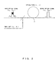
- the length of the optical fiber 11 is “L”, and the loss is " ⁇ ”. Also given is that the polarization states of all light waves are equal, and phases match completely in the optical fiber 11.
- the input power P p (0) of the pump light E p is assumed to be sufficiently larger than the power P s of the optical signal E s and the power P c of the idler light E c . In this description, “sufficiently larger” is defined as ten times larger (10 dB) or more, for example.
- the optical signal E 5 output from the optical fiber 11 can acquire gain G s as shown in the following equation (1):
- ⁇ (L) represents nonlinear optical phase shift
- P p (0) represents input power of the pump light
- ⁇ represents third-order nonlinear constant
- n2 and “A eff” represents a nonlinear refractive index and an effective core cross-section area, respectively, in the optical fiber 11.
- the optical parametric gain G 5 increases in proportion to squared product of the nonlinear constant, the input power of the pump light, and the interaction length.
- the generation efficiency of the four-wave mixing is highly dependent on the polarization state of the interacting light waves. Specifically, when the polarization states of light waves inputted to the optical fiber 11 are the same, the generation efficiency of the four-wave mixing is maximized, but when the polarization states of the light waves are orthogonal to each other, the four-wave mixing hardly occurs.
- the optical signal E s is parametrically amplified selectively in the same polarization state as that of the pump light E p .
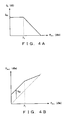
- Fig. 4A and Fig. 4B are diagrams showing the parametric gain and the output power of the optical signal with respect to input power. In this drawing, it is assumed that the input power of the pump light E p is constant.
- the parametric gains G s reaches saturation and starts to decrease, as shown in Fig. 4A.
- the output power of the optical signal P s-out approaches the state represented by the dotted line as shown in Fig. 4B.
- Fig.5 and Fig. 6 are diagrams explaining the relation between the gain saturation and waveform shaping.
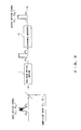
- Fig. 5 schematically shows the waveform of the input signal/output signal when the input power of the optical signal is smaller than the threshold power P 1 .
- the output power of the optical signal is approximately proportional to the input power of the optical signal. If intensity noise is added to the input optical signal, the intensity noise is also amplified and outputted.
- Fig. 6 schematically shows the waveform of the input signal/output signal when the input power of the optical signal is larger than the threshold power P 1 .
- the output waveform shown by a dotted line represents output power under the assumption that the gain was not saturated.
- the output waveform shown by a solid line represents output power when the gain saturation occurs, and it is the actual output waveform of the optical waveform shaping apparatus of the embodiment.
- the parametric gain in the optical fiber 11 reaches saturation when the pump light enters the depletion state. Therefore, the output power of the optical signal is suppressed compared to the case that operates under the assumption that the gain was not saturated. In other words, in this case, the optical limiter function is performed. At the same time, the intensity noise of the "1" level of the optical signal is also suppressed. Thus, "1" level noise is removed and the waveform of the optical signal outputted from the optical fiber 11 is favorably shaped.
- the output level in a case in which the input power of the optical signal exceeds the threshold power P 1 and the gain is saturated is basically higher than the output level in a case in which the input power of the optical signal is smaller than the threshold power P 1 and the gain is not saturated.
- the intensity noise of the optical signal may be suppressed.
- the parametric amplification is an efficient amplification method which increases in proportion to the square of the pump light power, approximately.
- a configuration in which an optical signal is processed in the state in which the parametric gain is saturated is not favorable in general.
- a configuration in which the pump light is in depletion state has not been employed previously because gain efficiency is extremely reduced.
- the optical waveform shaping apparatus of the embodiment of the present invention introduces a configuration in which strong gain saturation (due to depletion of the pump light) is employed in order to achieve the optical limiter function. By so doing, a favorable waveform shaping effect can be obtained.
- the waveform shaping circuits described in the Patent Document 1 and the Patent Document 2 provide the optical limiter function by utilizing four-wave mixing.
- those circuits do not use pump light for amplifying the optical signal, and thus they do not utilize "saturation of gain.”
- the circuits reduce (i. e. , limit) the power of the optical signal by transferring the power of the optical signal to probe light. Therefore, the optical limiter function of the Patent Documents is weak and the "1" level intensity noise may not be suppressed sufficiently.
- the optical waveform shaping apparatus of an embodiment of the present invention operates under the premise of a configuration in which an optical signal is amplified by using pump light.
- the optical limiter function is realized by gain saturation due to the pump light depletion.
- the parametric gain as represented in the above equations (1)-(3), depends on the square of an interaction length. Therefore, when the pump light enters a depletion state, the parametric gain is drastically reduced and sufficient optical limiter function can be obtained accordingly. For that reason, the optical waveform shaping apparatus of the embodiment can perform favorable waveform shaping.
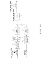
- Fig. 7 is a diagram showing a specific configuration of the optical waveform shaping apparatus of the embodiment of the present invention.
- the nonlinear optical medium 1 is a second-order or third-order nonlinear optical medium ( ⁇ (2) / ⁇ (3) ) and it can be realized by the above optical fiber 11, for example.
- a polarization controller 21 controls the polarization state of an input optical signal.
- a polarization controller 22 controls the polarization state of pump light. Note that each of the polarization controllers 21 and 22 controls the polarization state of the optical signal and the pump light in accordance with the instruction from a polarization control circuit 27.
- a wavelength-plate type polarization controller, a LiNbO 3 type polarization controller, a fiber sqeezing type polarization controller, a Faraday rotator, and other implements can be used.
- a power controller 23 adjusts the power of the optical signal having the polarization state controlled by the polarization controller 21.
- a power controller 24 adjusts the power of the pump light having the polarization state controlled by the polarization controlled 22. Note that each of the power controllers 23 and 24 controls the power of the optical signal and the pump light in accordance with the instruction from a power control circuit 28.
- the power controllers 23 and 24 can be realized by, for example, an optical amplifier (or a combination of an optical amplifier and an optical attenuator), among others.
- a monitor circuit 25 monitors the power of the optical signal inputted to the nonlinear optical medium 1 and the power of the optical signal output from the nonlinear optical medium 1. Note that the monitor circuit 25 detects the power of the optical signal input to the nonlinear optical medium 1 by receiving a part of the light wave (including the optical signal and the pump light) input to the nonlinear optical medium 1. In the same manner, the monitor circuit 25 detects the power of the optical signal output from the nonlinear optical medium 1 by receiving a part of the light wave (including the optical signal and the pump light) output from the nonlinear optical medium 1.
- a comparator circuit 26 calculates a gain in the nonlinear optical medium 1 based on the input power and the output power of the optical signal.
- the comparator circuit 26 compares the input power and/or output power of the optical signal with a prescribed threshold, respectively, when necessary.
- the polarization control instruction circuit 27 refers to the output of the comparator circuit 26, and issues instructions to adjust the polarization to the polarization controllers 21 and 22.
- the power control instruction circuit 28 refers to the comparator circuit 26, and issues instructions to adjust optical power to the power controllers 23 and 24.
- the optical waveform shaping apparatus with the above configuration comprises a pump light source and an optical band pass filter, however they are not shown in the drawing.
- the pump light source generates the pump light (CW light beam or optical pulses). If the optical pulse is used as the pump light, a pulse train synchronized with a clock signal recovered from input optical signal may be generated, for example.
- the optical band pass filter is, for example, an optical wavelength filter having a transmission frequency that is the same as the wavelength of the optical signal and is provided to the subsequent stage of the nonlinear optical medium 1.
- the optical band pass filter extracts a wavelength component of the optical signal from the output of the nonlinear optical medium 1.
- the polarization controllers 21 and 22 and the power controllers 23 and 24 are adjusted in accordance with the following procedure.
- the states of the polarization controllers 21 and 22 are adjusted.
- the polarization states of the optical signal and the pump light are adjusted so that the nonlinear optical effect is appropriately generated in the nonlinear optical medium 1.
- the nonlinear optical effect (especially, four-wave mixing) occurs with the maximum efficiency when the polarization states of the optical signal and the pump light are identical. Therefore, the polarization controllers 21 and 22 may be controlled so that the polarization states of the optical signal and the pump light match each other.
- the present invention is not limited to this configuration; the polarization states of the optical signal and the pump light may be controlled so as to differ from each other.
- the power control instruction circuit 28 adjusts the state of the power controller 24.
- the power of the pump light is controlled so that the desired or sufficient parametric gain can be obtained in the nonlinear optical medium 1.
- the input power of the optical signal is small, and the power of the pump light is significantly larger than the input power of the optical signal.
- the assumed state is such that the parametric gain approximately follows the above equation (1), for example.
- the input power of the optical signal is increased while monitoring the parametric gain in the nonlinear optical medium 1.
- the parametric gains is approximately constant.
- the power control instruction circuit 28 ends the adjustment of the power controller 23 at the point in time when the parametric gain is reduced by a prescribed level.
- the extent to which the parametric gain should be reduced depends on the required level of the optical limiter function (i.e. waveform shaping function). For example, in a system, in which the waveform of an input optical signal is estimated to be relatively favorable, slight reduction of the parametric gain may be sufficient, putting a high priority on efficiency of the gain rather than on the waveform shaping effect. On the other hand, in a system in which the waveform of an input optical signal is estimated to be considerably degraded, the parametric gain may be reduced significantly in order to obtain sufficient waveform shaping effect.
- the optical limiter function i.e. waveform shaping function
- the adjustment of the input power of the optical signal can be performed based on the power of the pump light output from the nonlinear optical medium 1.
- the optical limiter function for waveform shaping of the present invention is realized when the pump light is in the depletion state.
- the waveform shaping can be performed in the same manner as monitoring the parametric gain.
- the optical waveform shaping apparatus of the present invention is applied to an optical switch having an amplification function.
- This kind of optical switch is, for example, realized by providing a polarizer in the subsequent stage of the nonlinear optical medium 1 of the optical waveform shaping apparatus shown in Fig. 7.
- Fig. 8A-Fig. 8C are diagrams explaining operations of the optical switch of the first example.
- the optical signal E s (wavelength: ⁇ s , peak power: P s ) and optical control pulse E p (wavelength: ⁇ p , peak power: P p ) serving as the pump light, are input to an optical fiber (HNLF) 31 serving as the nonlinear optical medium.
- HNLF optical fiber
- a polarizer 32 is provided in the subsequent stage of the optical fiber 31.
- a linear polarization component in a direction of the polarization main axis of the polarizer 32 alone in the optical signal output from the optical fiber 31 is transmitted through the polarizer 32.
- the polarization state of the optical signal E s is controlled, as shown in Fig. 8A, so as to be orthogonal to the polarization main axis of the polarizer 32 at the input side of the optical fiber 31.
- the polarization state of the optical signal E s does not change in the optical fiber 31.
- the polarization direction of the optical signal E s output from the optical fiber 31 is still orthogonal to the polarization main axis of the polarizer 32.
- the optical signal E s is blocked by the polarizer 32.
- the polarization of the optical control pulse E p is controlled so as to be linear polarization at angle of 40-50 degrees (preferably 45 degrees) with respect to the polarization of the optical signal E s .
- the polarization state of the optical signal E s changes by influence of the optical control pulse E p in the optical fiber 31.
- peak power P p of the optical control pulse E p is sufficiently larger than the power P s of the optical signal E s .
- the optical signal E s is parametrically amplified in a polarization direction of the optical control E p in the optical fiber 31.
- the optical signal E s output from the optical fiber 31 includes a large polarization component in a direction of the polarization main axis of the polarizer 32. Therefore, in a time domain where the optical control pulse E p is present, a part of the components of the optical signal E 5 is transmitted through the polarizer 32. As above, the optical signal E 5 is switched according to the presence or absence of the optical control E p .
- the optical waveform shaping apparatus of the embodiment can shape the waveform of an ultrahigh speed optical signal of several tera bits per second (Tb/s).
- the optical waveform shaping apparatus of the second example comprises a saturable absorber 41 in the previous or subsequent stage of the nonlinear optical medium 1 of the above waveform shaping apparatus, as shown in Fig. 9.
- the saturable absorber 41 suppresses the OFF level fluctuation of an optical signal.
- the saturable absorber 41 can be realized by a semiconductor amplifier, a Mach-Zehnder interferometer optical fiber switch, a nonlinear optical loop mirror (NLOM) switch, or similar means, for example.
- One of the causes of quality deterioration of a phase-modulated optical signal or a frequency-modulated optical signal is such that intensity noise (and intensity fluctuation) is converted into phase noise by the nonlinear optical effect in an optical fiber. Therefore, suppression of the intensity noise (and intensity fluctuation) of an optical signal by using the optical waveform shaping apparatus of the present invention is effective for quality improvement of a phase-modulated optical signal or a frequency-modulated optical signal.
- Fig. 10 is an example where the optical waveform shaping apparatus of the present invention is applied to a communication apparatus for optical communication system (e.g. an optical receiver or optical repeater).
- a communication apparatus for optical communication system e.g. an optical receiver or optical repeater.
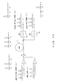
- a system in which an optical DPSK signal is transmitted via an optical fiber transmission path is introduced. Assume that the optical wavelength of the optical DPSK signal is " ⁇ s ".
- an optical DPSK signal and pump light are input to the above nonlinear optical medium 1.
- an idler wave (four-wave mixing light) having the wavelength ⁇ c is generated by four-wave mixing in the nonlinear optical fiber 1.
- phase of the optical DPSK signal (zero/ ⁇ ) and phase of the idler wave ( ⁇ /zero) are inverted from each other.
- the optical output (including the optical DPSK signal and an idler wave) is split by an optical splitter, and one portion is guided to an optical band pass filter 51 and the other portion is guided to an optical band pass filter 52.
- the optical band pass filter 51 transmits a frequency component ⁇ s . That is, the optical DPSK signal is obtained from the output of the optical band pass filter 51.
- the optical band pass filter 52 transmits a frequency component ⁇ c . That is, an idler wave signal is obtained from the output of the optical band pass filter 52. Consequently, by detecting (or demodulating) the optical DPSK signal or the idler wave, transmitted information can be recovered.
- Fig. 10 shows a configuration using a pulse train synchronized with an optical DPSK signal as pump light; however, the present invention is not limited to the configuration.
- a continuous wave beam with high power sufficient to obtain a desired parametric gain may be used as the pump light.
- an optical pulse train having flattened-top shape may be used as pump light.
- an input optical signal is applied with an optical phase modulation by cross phase modulation (XPM).
- the intensity of the cross phase modulation is proportional to the peak intensity of the pump light. For that reason, if the pump light is a short pulse with a large peak, there is a probability that the optical phase of the optical signal is disturbed.
- the configuration of the fourth example uses a pump light pulse train with flattened-top shape as pump light. In a time domain where the power of the pump light is constant, influence of the cross phase modulation is maintained at a constant level, and as a result, the optical phase disturbance can be suppressed.
- a demodulator 61 for converting the optical signal into an intensity-modulated optical signal may be provided in the previous stage of the optical waveform shaping apparatus of the present invention. According to this configuration, the phase-modulated optical signal or the frequency-modulated optical signal is shaped after being converted into an intensity-modulated optical signal.
- a demodulator for converting an optical DPSK signal into an intensity-modulated optical signal can be realized by using a 1-bit delay element 62.
- a demodulator for converting an optical FSK signal into an intensity-modulated optical signal can be realized by using a band pass filter 63-1 having a transmission frequency f 1 and a band pass filter 63-2 having a transmission frequency f 2 . Note that the optical FSK signal shown in Fig. 13B is such that each of the frequencies f 1 and f 2 is assigned to "1" or "0".
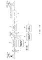
- FIG. 14 A configuration for waveform shaping without depending on the polarization state of an input optical signal is shown in Fig. 14.
- a polarization of the input optical signal is fixed at an arbitrary polarization (e.g., linear polarization or elliptical polarization) by the polarization controller 21. In other words, fluctuation of the polarization of the input optical signal is removed.
- the power controller 23 controls the power of the optical signal with the fixed polarization.
- a polarization of the pump light is fixed by the polarization controller 22, and the power is controlled by the power controller 24.
- the polarization of the pump light may be the same as, or may be different from, that of the optical signal.
- polarization controllers 21 and 22 and the power controllers 23 and 24 are based on the procedures explained with reference to Fig. 7.
- a polarizer 71 (or PBS: Polarizing Beam Splitter) is provided between the polarization controller 21 and the power controller 23.
- a control system not shown in the drawing monitors the output power of the polarizer 71.
- the polarization controller 21 may be adjusted so as to maximize the output power of the polarizer 71.
- FIG. 15 A configuration designed to be independent of the polarization state of an input optical signal in a method that differs from that of the sixth example is set forth in Fig. 15.
- This optical waveform shaping apparatus avoids dependency on the polarization state of an input optical signal by using polarization diversity.
- PBS 81 splits an input optical signal into a pair of polarization components orthogonal to each other.
- the pair of the polarization components is incident to polarization controllers 82 and 83.
- the polarization controllers 82 and 83 convert each polarization component into linear polarizations in the same direction.
- a optical coupler 84 combines power the pair of linear polarizations output from the polarization controllers 82 and 83 and directs the combined component to the power controller 23.
- an optical circuit 85 for time adjustment may be provided in order to match the timing of the pair of linear polarization as necessary.
- the optical circuit 85 can be realized by an optical delay element or a Faraday rotator, for example. Note that controls of the polarization controllers 82, 83, and 22, and power controllers 23 and 24 are basically the same as the procedures explained with reference to Fig. 7.
Landscapes
- Physics & Mathematics (AREA)
- Electromagnetism (AREA)
- Engineering & Computer Science (AREA)
- Computer Networks & Wireless Communication (AREA)
- Signal Processing (AREA)
- Optical Modulation, Optical Deflection, Nonlinear Optics, Optical Demodulation, Optical Logic Elements (AREA)
Applications Claiming Priority (1)
| Application Number | Priority Date | Filing Date | Title |
|---|---|---|---|
| JP2006089434A JP5027434B2 (ja) | 2006-03-28 | 2006-03-28 | 光信号の波形を整形する装置 |
Publications (3)
| Publication Number | Publication Date |
|---|---|
| EP1841100A2 true EP1841100A2 (fr) | 2007-10-03 |
| EP1841100A3 EP1841100A3 (fr) | 2008-01-23 |
| EP1841100B1 EP1841100B1 (fr) | 2014-10-15 |
Family
ID=38180283
Family Applications (1)
| Application Number | Title | Priority Date | Filing Date |
|---|---|---|---|
| EP06019045.1A Ceased EP1841100B1 (fr) | 2006-03-28 | 2006-09-12 | Dispositif de mise en forme d'ondes optiques |
Country Status (3)
| Country | Link |
|---|---|
| US (1) | US7450298B2 (fr) |
| EP (1) | EP1841100B1 (fr) |
| JP (1) | JP5027434B2 (fr) |
Cited By (3)
| Publication number | Priority date | Publication date | Assignee | Title |
|---|---|---|---|---|
| EP2148242A1 (fr) | 2008-07-22 | 2010-01-27 | Fujitsu Limited | Dispositif de mise en forme d'ondes optiques indépendant de la polarisation |
| EP2224625A1 (fr) * | 2009-02-27 | 2010-09-01 | Fujitsu Limited | Dispositif de traitement de signaux optiques et procédé pour le traitement de signaux optiques |
| EP2187257A4 (fr) * | 2007-08-31 | 2011-08-24 | Fujitsu Ltd | Processeur de signaux optiques |
Families Citing this family (26)
| Publication number | Priority date | Publication date | Assignee | Title |
|---|---|---|---|---|
| US7453626B2 (en) * | 2007-03-01 | 2008-11-18 | The United States Of America As Represented By The Secretary Of Commerce | Four-wave mixing source of squeezed light for image processing and interferometry |
| JP5347333B2 (ja) | 2008-05-23 | 2013-11-20 | 富士通株式会社 | 光信号処理装置 |
| JP5136236B2 (ja) | 2008-06-19 | 2013-02-06 | 富士通株式会社 | 光受信装置 |
| JP2010079246A (ja) * | 2008-09-01 | 2010-04-08 | Furukawa Electric Co Ltd:The | 光波形再生器および光波形再生方法 |
| JP2010060656A (ja) * | 2008-09-01 | 2010-03-18 | Fujitsu Ltd | 偏光状態安定化方法及び装置、光信号処理システム |
| US7764423B2 (en) * | 2008-10-28 | 2010-07-27 | Alcatel-Lucent Usa Inc. | Polarization-independent four-wave mixing in a birefringent fiber |
| JP5381089B2 (ja) | 2008-12-25 | 2014-01-08 | 富士通株式会社 | 光信号処理装置 |
| JP5293269B2 (ja) * | 2009-02-27 | 2013-09-18 | 富士通株式会社 | 光雑音抑圧処理を用いた光ファイバ伝送システム及び方法 |
| WO2010125657A1 (fr) | 2009-04-28 | 2010-11-04 | 富士通株式会社 | Dispositif de traitement de signaux optiques |
| US8275263B1 (en) * | 2009-06-26 | 2012-09-25 | The Boeing Company | Multiplication of phase deviations |
| EP2495612B1 (fr) * | 2009-10-30 | 2019-11-27 | Fujitsu Limited | Dispositif de traitement de signal optique, récepteur, et système de réseau optique |
| JP5830872B2 (ja) * | 2010-03-19 | 2015-12-09 | 富士通株式会社 | 光信号処理装置、光通信方法、受信機、および光ネットワークシステム |
| US8705167B2 (en) * | 2010-08-25 | 2014-04-22 | Fujitsu Limited | System and method for compensating for polarization dependent loss |
| US20120219285A1 (en) * | 2011-02-28 | 2012-08-30 | David Jimmy Dahan | In-band optical signal to noise ratio monitoring technique |
| JP5751015B2 (ja) * | 2011-05-26 | 2015-07-22 | 富士通株式会社 | 光信号処理装置および光通信システム |
| GB2496214B (en) * | 2011-11-01 | 2016-03-16 | Fianium Ltd | Amplifying optical device pumped or seeded with nonlinearly generated light |
| US8989595B2 (en) * | 2013-06-19 | 2015-03-24 | Fujitsu Limited | Mitigation of optical signal to noise ratio degradation arising from polarization dependent loss |
| JP2017107073A (ja) * | 2015-12-10 | 2017-06-15 | キヤノン株式会社 | 光源装置およびそれを用いた情報取得装置 |
| US10008982B1 (en) * | 2016-02-19 | 2018-06-26 | Rockwell Collins, Inc. | Parametrically driven gyromagnetic nonlinear transmission line oscillator |
| US10673530B2 (en) * | 2016-10-05 | 2020-06-02 | LGS Innovations LLC Inc. | Free space optical communication system and method |
| JP7106835B2 (ja) * | 2017-10-06 | 2022-07-27 | 富士通株式会社 | 光伝送装置、波長変換装置、光伝送方法、および波長変換方法 |
| CA3093174C (fr) * | 2018-05-01 | 2025-05-13 | Xanadu Quantum Technologies Inc. | Dispositifs intégrés de génération de lumière comprimée |
| JP7099045B2 (ja) * | 2018-05-18 | 2022-07-12 | 富士通株式会社 | 波長変換装置、伝送装置、及び伝送システム |
| US10735128B1 (en) * | 2019-03-05 | 2020-08-04 | Rockwell Collins, Inc. | Optical phase sensitivity enhancement for reduced power |
| US11588295B2 (en) * | 2019-11-01 | 2023-02-21 | Ii-Vi Delaware, Inc. | Pump modulation for optical amplifier link communication |
| US11438086B2 (en) * | 2020-01-21 | 2022-09-06 | Fujitsu Limited | Optical amplification in an optical network |
Family Cites Families (20)
| Publication number | Priority date | Publication date | Assignee | Title |
|---|---|---|---|---|
| JP3419510B2 (ja) | 1992-10-16 | 2003-06-23 | 富士通株式会社 | 波長分散を補償した光通信システム及び該システムに適用可能な位相共役光発生装置 |
| US5400164A (en) * | 1993-09-10 | 1995-03-21 | At&T Corp. | Polarization-insensitive optical four-photon mixer |
| JP3494738B2 (ja) | 1994-10-20 | 2004-02-09 | 富士通株式会社 | 光位相共役を用いた光ファイバ通信システム |
| JP4011150B2 (ja) | 1996-04-11 | 2007-11-21 | 富士通株式会社 | 位相共役光の発生及び波長変換のための方法及び装置並びに該装置を有するシステム並びに該装置の製造方法 |
| DE69739862D1 (de) | 1996-08-22 | 2010-06-10 | Fujitsu Ltd | Faseroptisches Übertragungssystem mit optischer Phasenkonjugation |
| JP3461121B2 (ja) * | 1998-07-08 | 2003-10-27 | 日本電信電話株式会社 | 光リミッタ回路 |
| JP3566096B2 (ja) * | 1998-08-31 | 2004-09-15 | 富士通株式会社 | 位相共役変換及び波長変換のための装置 |
| US6501591B1 (en) * | 1999-01-07 | 2002-12-31 | Northwestern University | Tunable fiber optic parametric oscillator |
| US6344921B1 (en) * | 1999-02-22 | 2002-02-05 | Almantas Galvanauskas | Optical parametric amplifiers and generators in optical communication systems |
| JP2000323786A (ja) * | 1999-05-14 | 2000-11-24 | Fujitsu Ltd | 信号光の波形整形のための方法、装置及びシステム |
| JP3882979B2 (ja) * | 1999-10-15 | 2007-02-21 | 富士通株式会社 | 波形整形のための装置及びシステム |
| JP4454763B2 (ja) | 2000-03-03 | 2010-04-21 | 富士通株式会社 | 信号光を波形整形するための方法、装置及びシステム |
| US6717718B1 (en) * | 2001-03-14 | 2004-04-06 | Wayne Kelsoe | Hybrid optical device |
| EP1454436B1 (fr) * | 2001-08-16 | 2007-02-21 | Telefonaktiebolaget LM Ericsson (publ) | Amplificateur optique |
| JP4472222B2 (ja) | 2001-09-28 | 2010-06-02 | 富士通株式会社 | 信号光を波形整形するための方法、装置及びシステム |
| JP4094854B2 (ja) | 2002-01-09 | 2008-06-04 | 富士通株式会社 | 信号光を波形整形するための方法及び装置 |
| KR100617293B1 (ko) * | 2003-11-22 | 2006-08-30 | 한국전자통신연구원 | 파라메트릭 광증폭기를 위한 분산천이 광섬유 |
| US6961170B2 (en) * | 2004-03-19 | 2005-11-01 | Jeffrey Miller Hubbard | Optical parametric amplifier and method for implementing same |
| JP4451696B2 (ja) * | 2004-03-30 | 2010-04-14 | 富士通株式会社 | 微細構造ファイバの非線形係数の波長依存性をキャンセルする装置 |
| JP2007240389A (ja) * | 2006-03-09 | 2007-09-20 | Fujitsu Ltd | 光波形測定装置および光波形測定方法 |
-
2006
- 2006-03-28 JP JP2006089434A patent/JP5027434B2/ja not_active Expired - Fee Related
- 2006-09-12 EP EP06019045.1A patent/EP1841100B1/fr not_active Ceased
- 2006-09-14 US US11/520,727 patent/US7450298B2/en not_active Expired - Fee Related
Cited By (4)
| Publication number | Priority date | Publication date | Assignee | Title |
|---|---|---|---|---|
| EP2187257A4 (fr) * | 2007-08-31 | 2011-08-24 | Fujitsu Ltd | Processeur de signaux optiques |
| EP2148242A1 (fr) | 2008-07-22 | 2010-01-27 | Fujitsu Limited | Dispositif de mise en forme d'ondes optiques indépendant de la polarisation |
| US8041169B2 (en) | 2008-07-22 | 2011-10-18 | Fujitsu Limited | Optical signal processing device |
| EP2224625A1 (fr) * | 2009-02-27 | 2010-09-01 | Fujitsu Limited | Dispositif de traitement de signaux optiques et procédé pour le traitement de signaux optiques |
Also Published As
| Publication number | Publication date |
|---|---|
| EP1841100A3 (fr) | 2008-01-23 |
| US20070230518A1 (en) | 2007-10-04 |
| US7450298B2 (en) | 2008-11-11 |
| EP1841100B1 (fr) | 2014-10-15 |
| JP2007264319A (ja) | 2007-10-11 |
| JP5027434B2 (ja) | 2012-09-19 |
Similar Documents
| Publication | Publication Date | Title |
|---|---|---|
| EP1841100B1 (fr) | Dispositif de mise en forme d'ondes optiques | |
| EP2367051B1 (fr) | Dispositif de traitement de signaux optiques indépendant de la polarisation | |
| EP0703680B1 (fr) | Appareil et procédé de compensation de dispersion chromatique résultant de conjugaison de phase optique, ou conversion électro-optique d'autre type | |
| EP2083320B1 (fr) | Appareil de traitement de signaux optiques, appareil de réception optique et appareil de relais optique | |
| EP0776103B1 (fr) | Système de communication utilisant la conjugation de phase optique | |
| US5737110A (en) | Optical communication system using dark soliton lightwave | |
| JP5056095B2 (ja) | 光波形制御装置、光信号処理装置および光中継装置 | |
| EP2202898B1 (fr) | Dispositif de traitement de signaux optiques | |
| EP2124100B1 (fr) | Dispositif de traitement de signaux optiques | |
| EP2426553A1 (fr) | Dispositif de traitement de signaux optiques | |
| US8351110B2 (en) | Optical-signal processing apparatus |
Legal Events
| Date | Code | Title | Description |
|---|---|---|---|
| PUAI | Public reference made under article 153(3) epc to a published international application that has entered the european phase |
Free format text: ORIGINAL CODE: 0009012 |
|
| AK | Designated contracting states |
Kind code of ref document: A2 Designated state(s): AT BE BG CH CY CZ DE DK EE ES FI FR GB GR HU IE IS IT LI LT LU LV MC NL PL PT RO SE SI SK TR |
|
| AX | Request for extension of the european patent |
Extension state: AL BA HR MK YU |
|
| PUAL | Search report despatched |
Free format text: ORIGINAL CODE: 0009013 |
|
| AK | Designated contracting states |
Kind code of ref document: A3 Designated state(s): AT BE BG CH CY CZ DE DK EE ES FI FR GB GR HU IE IS IT LI LT LU LV MC NL PL PT RO SE SI SK TR |
|
| AX | Request for extension of the european patent |
Extension state: AL BA HR MK YU |
|
| 17P | Request for examination filed |
Effective date: 20080602 |
|
| AKX | Designation fees paid |
Designated state(s): DE FR GB |
|
| REG | Reference to a national code |
Ref country code: DE Ref legal event code: R079 Ref document number: 602006043343 Country of ref document: DE Free format text: PREVIOUS MAIN CLASS: H04B0010170000 Ipc: H04B0010299000 |
|
| RIC1 | Information provided on ipc code assigned before grant |
Ipc: H04B 10/299 20130101AFI20130912BHEP |
|
| GRAP | Despatch of communication of intention to grant a patent |
Free format text: ORIGINAL CODE: EPIDOSNIGR1 |
|
| INTG | Intention to grant announced |
Effective date: 20131022 |
|
| GRAP | Despatch of communication of intention to grant a patent |
Free format text: ORIGINAL CODE: EPIDOSNIGR1 |
|
| INTG | Intention to grant announced |
Effective date: 20140527 |
|
| GRAS | Grant fee paid |
Free format text: ORIGINAL CODE: EPIDOSNIGR3 |
|
| GRAA | (expected) grant |
Free format text: ORIGINAL CODE: 0009210 |
|
| AK | Designated contracting states |
Kind code of ref document: B1 Designated state(s): DE FR GB |
|
| REG | Reference to a national code |
Ref country code: GB Ref legal event code: FG4D |
|
| REG | Reference to a national code |
Ref country code: DE Ref legal event code: R096 Ref document number: 602006043343 Country of ref document: DE Effective date: 20141127 |
|
| REG | Reference to a national code |
Ref country code: DE Ref legal event code: R097 Ref document number: 602006043343 Country of ref document: DE |
|
| PLBE | No opposition filed within time limit |
Free format text: ORIGINAL CODE: 0009261 |
|
| STAA | Information on the status of an ep patent application or granted ep patent |
Free format text: STATUS: NO OPPOSITION FILED WITHIN TIME LIMIT |
|
| 26N | No opposition filed |
Effective date: 20150716 |
|
| REG | Reference to a national code |
Ref country code: FR Ref legal event code: PLFP Year of fee payment: 11 |
|
| REG | Reference to a national code |
Ref country code: FR Ref legal event code: PLFP Year of fee payment: 12 |
|
| PGFP | Annual fee paid to national office [announced via postgrant information from national office to epo] |
Ref country code: FR Payment date: 20170810 Year of fee payment: 12 Ref country code: DE Payment date: 20170905 Year of fee payment: 12 Ref country code: GB Payment date: 20170906 Year of fee payment: 12 |
|
| REG | Reference to a national code |
Ref country code: DE Ref legal event code: R119 Ref document number: 602006043343 Country of ref document: DE |
|
| GBPC | Gb: european patent ceased through non-payment of renewal fee |
Effective date: 20180912 |
|
| PG25 | Lapsed in a contracting state [announced via postgrant information from national office to epo] |
Ref country code: DE Free format text: LAPSE BECAUSE OF NON-PAYMENT OF DUE FEES Effective date: 20190402 |
|
| PG25 | Lapsed in a contracting state [announced via postgrant information from national office to epo] |
Ref country code: FR Free format text: LAPSE BECAUSE OF NON-PAYMENT OF DUE FEES Effective date: 20180930 |
|
| PG25 | Lapsed in a contracting state [announced via postgrant information from national office to epo] |
Ref country code: GB Free format text: LAPSE BECAUSE OF NON-PAYMENT OF DUE FEES Effective date: 20180912 |