EP1843357A2 - Vorrichtung und Verfahren zum Steuern eines Flash-Speichers - Google Patents
Vorrichtung und Verfahren zum Steuern eines Flash-Speichers Download PDFInfo
- Publication number
- EP1843357A2 EP1843357A2 EP07102842A EP07102842A EP1843357A2 EP 1843357 A2 EP1843357 A2 EP 1843357A2 EP 07102842 A EP07102842 A EP 07102842A EP 07102842 A EP07102842 A EP 07102842A EP 1843357 A2 EP1843357 A2 EP 1843357A2
- Authority
- EP
- European Patent Office
- Prior art keywords
- flash memory
- memory
- control information
- control
- stored
- Prior art date
- Legal status (The legal status is an assumption and is not a legal conclusion. Google has not performed a legal analysis and makes no representation as to the accuracy of the status listed.)
- Withdrawn
Links
Images


Classifications
-
- G—PHYSICS
- G06—COMPUTING OR CALCULATING; COUNTING
- G06F—ELECTRIC DIGITAL DATA PROCESSING
- G06F13/00—Interconnection of, or transfer of information or other signals between, memories, input/output devices or central processing units
- G06F13/14—Handling requests for interconnection or transfer
- G06F13/16—Handling requests for interconnection or transfer for access to memory bus
- G06F13/1668—Details of memory controller
- G06F13/1694—Configuration of memory controller to different memory types
-
- G—PHYSICS
- G06—COMPUTING OR CALCULATING; COUNTING
- G06F—ELECTRIC DIGITAL DATA PROCESSING
- G06F13/00—Interconnection of, or transfer of information or other signals between, memories, input/output devices or central processing units
- G06F13/38—Information transfer, e.g. on bus
- G06F13/42—Bus transfer protocol, e.g. handshake; Synchronisation
- G06F13/4204—Bus transfer protocol, e.g. handshake; Synchronisation on a parallel bus
- G06F13/4234—Bus transfer protocol, e.g. handshake; Synchronisation on a parallel bus being a memory bus
- G06F13/4239—Bus transfer protocol, e.g. handshake; Synchronisation on a parallel bus being a memory bus with asynchronous protocol
-
- G—PHYSICS
- G11—INFORMATION STORAGE
- G11C—STATIC STORES
- G11C16/00—Erasable programmable read-only memories
- G11C16/02—Erasable programmable read-only memories electrically programmable
- G11C16/06—Auxiliary circuits, e.g. for writing into memory
-
- G—PHYSICS
- G11—INFORMATION STORAGE
- G11C—STATIC STORES
- G11C7/00—Arrangements for writing information into, or reading information out from, a digital store
- G11C7/10—Input/output [I/O] data interface arrangements, e.g. I/O data control circuits, I/O data buffers
Definitions
- the present invention relates to controlling or operating flash memory. More particularly, but not exclusively, the present invention relates to controlling or operating flash memory that updates a flash memory's control information stored in a predetermined volatile memory when the type or format of flash memory is changed, and which controls the changed flash memory using the updated control information.
- a flash memory is a non-volatile computer memory that can be electrically erased and reprogrammed.
- Non-volatile computer memory is a memory that can be retained and stored, even when not powered.
- flash memory There are presently many types or formats of flash memory available ot the consumer.
- the contents of a flash memory can be erased and reprogrammed in terms of blocks.
- the flash memory is a modification of an Electrically Erasable Programmable Read-Only Memory (EEPROM). Unlike the EEPROM (in which the contents can be erased and corrected in terms of bytes),, a processing speed to erase and correct contents is high in the flash memory, since the contents are corrected in blocks.
- the flash memory is often used to store control codes, such as Basic Input/Output System (BIOS) of a Personal Computer (PC). When the BIOS needs to be corrected, the contents are recorded in blocks in the flash memory, not bytes, and thus the correction is easily performed.
- BIOS Basic Input/Output System
- the BIOS When the BIOS needs to be corrected, the contents are recorded in blocks in the flash memory, not bytes, and thus the correction is easily performed.
- the flash memory is not useful since addresses are assigned in bytes, not blocks.
- the flash memory obtains its name because a flash memory microchip is constructed such that portions of memory cells on a microchip can be erased by only one operation, like a flash. Erasure is typically performed by a Fowler-Nordheim tunneling effect. That is, electrons pass through a thin dielectric material and eliminate charges from floating gates respectively connected to the memory cells.
- the flash memory is an active device that receives commands from a programmer and executes the commands; it is not a passive device that merely has a storage device, a refresh circuit, and an error correction circuit, such as Dynamic RAM (DRAM).
- Commands are issued by a Command User Interface (CUI), and the status of the system is managed by a Write State Machine (WSM).
- the kind of the commands to be provided include a reading command, a writing command, and other control commands.
- FIG. 1 is a diagram showing a known flash memory control system.
- the flash memory control system has a flash memory controller 10 and a flash memory 20.
- the flash memory controller 10 has a core processor 11, a One Time Programmable (OTP) memory 12, a status checking unit 13, and a control code transmitting unit 14.
- OTP One Time Programmable
- the OTP memory 12 stores control codes for controlling the flash memory 20.
- the control codes include a reading control code, a writing control code, a reset control code, a block locking control code, and the like.
- the status checking unit 13 checks the status of the flash memory 20. That is, the status checking unit 13 checks whether the flash memory 20 is in an active mode or in a standby mode.
- the control code transmitting unit 14 transmits the control codes stored in the OTP memory 12 to the flash memory 20.
- the core processor 11 refers to the status of the flash memory 20 checked by the status checking unit 13 so as to extract a control code from the OTP memory 12, and causes the control code transmitting unit 14 to transmit the extracted control code. Then, the core processor 11 performs the overall control of the OTP memory 12, the status checking unit 13, and the control code transmitting unit 14.
- an additional flash memory controller including an OTP memory, in which corresponding control codes are stored is required, which leads to an increase in costs.
- a memory system that includes a memory controller controlling an access to a non-volatile memory and a volatile memory in response to a memory request and having a memory storing address information of data stored in the volatile memory, a NAND flash memory, and a RAM storing data of the NAND flash memory.
- an apparatus for controlling a flash memory including a flash memory storing its own control information, a first memory storing a programming code for controlling the flash memory, a control unit generating a control code for controlling the flash memory by assigning the control information to the programming code, and a transceiver transmitting the control code.
- a method of controlling a flash memory including receiving control information from a flash memory, generating a control code for controlling the flash memory by assigning the control information to the programming code, and transmitting the control code.
- a flash memory device arranged to store computer readable information, wherein the device is further arranged to store control information useable by a flash memory controller for controlling the flash memory device.
- the control information can be stored in a predetermined location in the flash memory.
- FIG. 2 is a block diagram showing an apparatus for controlling or operating a flash memory according to an exemplary embodiment of the present invention.
- An apparatus for controlling a flash memory (hereinafter, referred to as "flash memory control apparatus") 100 includes a flash memory control unit 200 and a flash memory 300.
- the flash memory control unit 200 includes a control information receiving unit 210, a control unit 220, a status checking unit 230, a first memory 240, a second memory 250, and a transceiver 260.
- the flash memory 300 stores its own control information.
- the flash memory 300 is a non-volatile memory to which power can be continuously supplied, and the contents of the flash memory can be erased and reprogrammed in terms of blocks.
- the control information is information required for controlling the flash memory 300 and includes at least one of the number of dies, the number of planes by dies, the number of blocks, the size of a page, the number of pages by blocks, the number of sectors by pages, a position of a bad mark, supportability of a cache operation, and supportability of a copy back operation.
- control information includes information for operations of reading data from the flash memory 300, writing data into the flash memory 300, erasing data of the flash memory 300, resetting the flash memory 300, and locking blocks in the flash memory 300.
- the locking of blocks means the limit of an access to the blocks such that the reading operation of the stored data or other commands are not executed while data is being written into the flash memory 300 or while the data of the flash memory 300 is being erased.
- the first memory 240 stores a programming code for controlling the flash memory 300.
- the programming code is a code for reading, writing, or other controls for the flash memory 300. In order to allow this code to be applied to all types or formats of flash memories, and not just to a specific flash memory, information peculiar to the flash memory may not be included.
- the first memory 240 may store control information for a specified flash memory arbitrarily selected by a user. For example, control information for one specified flash memory that is frequently used by the user is stored in the first memory 240, such that a process of storing the control information stored in the flash memory into the second memory 250 may be omitted.
- the first memory 240 may store control information for a plurality of specified flash memories.
- the first memory 240 is preferably a non-volatile memory. More preferably, in view of a reduction in costs, an OTP (One Time Programmable) memory can be used.
- OTP One Time Programmable
- the programming code stored in the first memory 240 and the control information of the specified flash memory may not be updated.
- the second memory 250 temporarily stores the control information of flash memory 300.
- the control information of flash memory 300 may be received from the flash memory 300 or may be separately input.
- the control information stored in the flash memory 300 may be received and temporarily stored in the second memory 250 in order to control the flash memory 300.
- the control information, which is input in order to update the flash memory 300 may be temporarily stored prior to being transmitted to the flash memory 300.
- the control unit 220 generates a control code for controlling the flash memory 300 by assigning the control information to the programming code from the first memory 240.
- the control information may be one stored in the first memory 240, one stored in the second memory 250, or one extracted directly from the flash memory 300.
- control unit 220 compares the control information stored in the flash memory 300 and the control information stored in the first memory 240 and then, when both are consistent with each other, generates the control code by assigning the control information stored in the first memory 240 to the programming code. When both are inconsistent with each other, the control unit 220 generates the control code by assigning the control information extracted from the flash memory 300 to the programming code.
- the control unit 220 first compares, as described above, the control information stored in the flash memory 300 and the control information stored in the first memory 240 and then, when both are consistent with each other, generates the control code by assigning the control information stored in the first memory 240 to the programming code. When both are inconsistent with each other, the control unit 220 generates the control code by storing the control information extracted from the flash memory 300 in the second memory 250 and then assigning the control information stored in the second memory 250 to the programming code.
- control unit 220 performs the overall control of the control information receiving unit 210, the status checking unit 230, the first memory 240, the second memory 250, the transceiver 260, the flash memory 300, and the flash memory control apparatus 100.
- the transceiver 260 transmits the control code generated by the control unit 220 to the flash memory 300. Further, the transceiver 260 receives the control information of the flash memory 300 for storing the control information stored in the flash memory 300 in the second memory 250, and transmits updated control information for updating the flash memory 300 to the flash memory 300.
- the control information receiving unit 210 receives new control information for updating the flash memory 300.
- the received control information may be directly transmitted to the flash memory 300 through the transceiver 260 or may be temporarily stored in the second memory 250 and then transmitted to the flash memory 300. If the flash memory 300 is updated, the updated flash memory 300 stores the new control information. Subsequently, upon the control of the updated flash memory 300, a control code corresponding to the new control information is generated by the control unit 220 and then transmitted to the updated flash memory 300.
- the status checking unit 230 checks the status of the flash memory 300. That is, the status checking unit 230 checks whether the flash memory 300 is executing the reading operation, the writing operation, or other control operations.
- the control unit 220 refers to the status of the flash memory 300 checked by the status checking unit 230 and decides whether to transmit the control code to the flash memory 300.
- Figure 3 is a diagram showing a flash memory, in which control information is stored, according to an exemplary embodiment of the present invention.
- the flash memory 300 may be divided into a large block flash memory 310 and a small block flash memory 320, and thus the arrangement of sectors included in each block may be changed. That is, a plurality of sectors exist on one page in case of the large block flash memory 310, while one sector exists on one page in case of the small block flash memory 320.
- control information of flash memory 300 is preferably stored in the first sector 313 or 323 on the first page 312 or 322 of the first block 311 or 321. This is because, when the control information of the flash memory 300 is stored at an arbitrary position, the flash memory control unit 200 may not recognize the control information of the flash memory 300 and thus, may not transmit the control code for extracting the control information.
- control information may be stored at an arbitrary position set by a user.
- the flash memory control unit 200 may extract the control information for a flash memory at a position set by the user.
- the flash memory 300 that stores the control information may store and update other data using only regions excluding a region where the control information is stored.
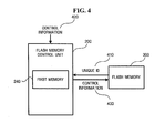
- Figure 4 is a conceptual diagram showing an example where control information is transmitted to a flash memory, according to an exemplary embodiment of the present invention.
- control information 430 may be inserted into the flash memory 300.
- the control information 430 may be inserted using the flash memory control unit 200. Specifically, first, the control information receiving unit 210 of the flash memory control unit 200 receives the control information 420. Then, the received control information 420 is temporarily stored in the second memory 250, and the temporarily stored control information 420 is transmitted to the flash memory 300 through the transceiver 260.
- control information 420 may be stored in the first sector 313 or 323 on the first page 312 or 322 of the first block 311 or 321 or may be stored at a separate position set by the user.
- the flash memory control unit 200 may insert the control information for all flash memories, as well as the specified flash memory. Accordingly, a connection device that connects the transceiver 260 and the flash memory 300 is preferably a device by which the connection and disconnection of the flash memory 300 is easily performed. Then, the flash memory control unit 200 receives the control information 420 corresponding to the connected flash memory 300 from the user and inserts it into the flash memory 300.
- the flash memory control unit 200 may insert the control information for the specified flash memory stored in the first memory 240 into a predetermined region of the connected flash memory 300.
- the control information stored in the first memory 240 may be the control information for a plurality of specified flash memories. That is, a plurality of different control information is stored in the first memory 240.
- the flash memory control unit 200 may extract control information 430 to be transmitted using the unique ID 410 of the flash memory 300 received from the flash memory 300.
- the flash memory 300 transmits its own unique ID 410 upon the connection to the flash memory control unit 200, and the flash memory control unit 200 that receives the unique ID 410 checks whether or not the control information corresponding to the unique ID 410 is stored in the first memory 240. Then, when the corresponding control information exists, the flash memory control unit 200 extracts the corresponding control information and transmits the extracted control information to the flash memory 300. When the corresponding control information does not exist, the flash memory control unit 200 transmits, to the flash memory 300, the control information 420 that is input from the user through the control information receiving unit 210.
- the flash memory 300 may be divided into the large block flash memory 310 and the small block flash memory 320, and writing methods for the flash memories 310 and 320 may be different. Accordingly, when inserting the control information 430 into the flash memory 300, the flash memory control unit 200 may test two methods corresponding to the kinds of the flash memory 300.
- Figure 5 is a conceptual diagram showing an example where control information is stored in the second memory 250, according to an exemplary embodiment of the present invention.
- the flash memory control unit 200 In order to control the flash memory 300, the flash memory control unit 200 first receives a unique ID 510 from the flash memory 300. Then, the flash memory control unit 200 checks whether or not control information corresponding to the received unique ID 510 is stored in the first memory 240, and if the corresponding control information is stored, the flash memory control unit 200 generates the control code for the connected flash memory 300 using the stored control information and the programming code, and controls the flash memory 300 using the generated control code.
- the flash memory control unit 200 extracts control information 520 stored in a predetermined region of the flash memory 300.
- the flash memory control unit 200 may extract the control information 520 from the first sector 313 or 323 on the first page 312 or 322 of the first block 311 or 321 in the storage region of the flash memory 300, or may extract the control information 520 from a prescribed position. Then, the extracted control information 520 is stored in the second memory 250 in order to control the flash memory 300.
- the flash memory 300 may be divided into the large block flash memory 310 and the small block flash memory 320, and reading methods for the flash memories 310 and 320 may be different. Accordingly, when extracting the control information 520 from the flash memory 300, the flash memory control unit 200 may test two methods corresponding to the kinds of the flash memory 300.
- Figure 6 is a flowchart showing a process of controlling a flash memory according to an exemplary embodiment of the present invention.
- the transceiver 260 of the flash memory control unit 200 first receives a unique ID from the flash memory 300 (Operation S610).
- the received unique ID is transmitted to the control unit 220, and the control unit 220 checks whether or not control information corresponding to the unique ID exists among control information for a plurality of specified flash memories stored in the first memory 240 (Operation S620).
- the specified flash memory is a flash memory arbitrarily selected by a user. For example, control information for a flash memory that is requested by the user is stored in the first memory 240, such that a process of storing the control information of the flash memory in the second memory 250 may be omitted.
- the first memory 240 is a non-volatile memory, and more preferably, an OTP memory.
- the control information includes at least one of the number of dies, the number of planes by dies, the number of blocks, the size of a page, the number of pages by blocks, the number of sectors by pages, a position of a bad mark, supportability of a cache operation, and supportability of a copy back operation.
- control unit 220 If the corresponding control information is stored, the control unit 220 generates the control code using the corresponding control information and the programming code stored in the first memory 240 (Operation S650).
- the status checking unit 230 checks the status of the flash memory 300. That is, the status checking unit 230 checks whether the flash memory 300 is executing a reading operation or writing operation, and the status check result is sent to the control unit 220 (S660).
- control unit 220 reserves the transmission of the control code when the flash memory 300 is operating, or transmits the control code through the transceiver 260 when the flash memory 300 is not operating (Operation S670).
- the transceiver 260 extracts the control information from the flash memory 300 (Operation S630). Next, the extracted control information is stored in the second memory 250 as a volatile memory (Operation S640).
- control unit 220 If the control information is stored in the second memory 250, the control unit 220 generates the control code for controlling the flash memory 300 using the programming code stored in the first memory 240 and the control information stored in the second memory 250 (Operation S650).
- control unit 220 refers to the status of the flash memory 300 checked by the status checking unit 230 (Operation S660) and, when the flash memory 300 is operating, transmits the generated control code through the transceiver 260 ( Operation S670).
- each block of the block diagram of Figure 2 and combinations of operations in the flowchart of Figure 6 can be implemented by computer program instructions.
- These computer program instructions can be provided to a processor of a general-purpose computer, special purpose computer, or other programmable data processing apparatus to produce a machine, such that the instructions, which execute via the processor of the computer or other programmable data processing apparatus, create means for implementing the functions specified in the flowchart block or blocks.
- These computer program instructions may also be stored in a computer usable or computer-readable memory that can direct a computer or other programmable data processing apparatus to function in a particular manner, such that the instructions stored in the computer usable or computer-readable memory produce an article of manufacture including instruction means that implement the function specified in the flowchart block or blocks.
- the computer program instructions may also be loaded onto a computer or other programmable data processing apparatus to cause a series of operational steps to be performed on the computer or other programmable apparatus to produce a computer implemented process such that the instructions that execute on the computer or other programmable apparatus provide steps for implementing the functions specified in the flowchart block or blocks.
- each block of the block diagrams may represent a module, segment, or portion of code, which includes one or more executable instructions for implementing the specified logical function(s). It should also be noted that in some alternative implementations, the functions noted in the blocks may occur out of order. For example, two blocks shown in succession may in fact be executed substantially concurrently or the blocks may sometimes be executed in reverse order depending upon the functionality involved.
- control information of the flash memory stored in a predetermined volatile memory can be updated whenever the kind of the flash memory is changed, and the changed flash memory can be controlled using the updated control information. Therefore, costs for providing an additional flash memory controller according to the kind of the changed flash memory can be saved.
- control information can be extracted from the flash memory that stores the control information, and the flash memory can be controlled using the extracted control information. Therefore, control for different flash memories can be simply performed.
Landscapes
- Engineering & Computer Science (AREA)
- Theoretical Computer Science (AREA)
- Physics & Mathematics (AREA)
- General Engineering & Computer Science (AREA)
- General Physics & Mathematics (AREA)
- Techniques For Improving Reliability Of Storages (AREA)
- Read Only Memory (AREA)
- Memory System (AREA)
Applications Claiming Priority (1)
| Application Number | Priority Date | Filing Date | Title |
|---|---|---|---|
| KR1020060017771A KR100746036B1 (ko) | 2006-02-23 | 2006-02-23 | 플래시 메모리를 제어하는 장치 및 방법 |
Publications (2)
| Publication Number | Publication Date |
|---|---|
| EP1843357A2 true EP1843357A2 (de) | 2007-10-10 |
| EP1843357A3 EP1843357A3 (de) | 2010-10-06 |
Family
ID=38370498
Family Applications (1)
| Application Number | Title | Priority Date | Filing Date |
|---|---|---|---|
| EP07102842A Withdrawn EP1843357A3 (de) | 2006-02-23 | 2007-02-21 | Vorrichtung und Verfahren zum Steuern eines Flash-Speichers |
Country Status (5)
| Country | Link |
|---|---|
| US (1) | US7809878B2 (de) |
| EP (1) | EP1843357A3 (de) |
| JP (1) | JP2007226798A (de) |
| KR (1) | KR100746036B1 (de) |
| CN (1) | CN101025711B (de) |
Families Citing this family (8)
| Publication number | Priority date | Publication date | Assignee | Title |
|---|---|---|---|---|
| WO2006101123A1 (ja) * | 2005-03-23 | 2006-09-28 | Matsushita Electric Industrial Co., Ltd. | 不揮発性記憶装置及び不揮発性記憶装置の制御情報のロード方法 |
| CN101751338B (zh) * | 2008-12-15 | 2012-03-07 | 中芯国际集成电路制造(上海)有限公司 | 数据存取控制装置及数据存取方法 |
| US8423722B1 (en) * | 2011-08-26 | 2013-04-16 | Western Digital Technologies, Inc. | System and method for high performance command processing in solid state drives |
| KR102491068B1 (ko) | 2017-11-17 | 2023-01-19 | 에스케이하이닉스 주식회사 | 메모리 장치에 대한 태스크들을 스케줄링하는 반도체 장치 및 이를 포함하는 시스템 |
| CN108595124A (zh) * | 2018-04-27 | 2018-09-28 | 江苏华存电子科技有限公司 | 一种提升多颗闪存平行写入校能的管理方法 |
| US11636173B2 (en) | 2019-03-28 | 2023-04-25 | SK Hynix Inc. | Method for candidate selection and accelerator for performing candidate selection |
| KR20200115102A (ko) | 2019-03-28 | 2020-10-07 | 에스케이하이닉스 주식회사 | 유사도에 따라 후보 선택을 가속하는 방법 및 후보 선택을 수행하는 가속기 |
| CN119127749B (zh) * | 2024-11-08 | 2025-02-18 | 湖南进芯电子科技有限公司 | 闪存接口电路、闪存控制方法、电子设备及存储介质 |
Citations (3)
| Publication number | Priority date | Publication date | Assignee | Title |
|---|---|---|---|---|
| US20030156473A1 (en) | 2001-09-28 | 2003-08-21 | Sinclair Alan Welsh | Memory controller |
| US20040062126A1 (en) | 2001-02-27 | 2004-04-01 | Fujitsu Limited | Memory system |
| US20050160218A1 (en) * | 2004-01-20 | 2005-07-21 | Sun-Teck See | Highly integrated mass storage device with an intelligent flash controller |
Family Cites Families (18)
| Publication number | Priority date | Publication date | Assignee | Title |
|---|---|---|---|---|
| JP3259232B2 (ja) | 1992-07-06 | 2002-02-25 | 清水建設株式会社 | カードによる入退管理システム |
| JPH06250827A (ja) * | 1993-02-23 | 1994-09-09 | Nippon Steel Corp | コンピュータシステム |
| JP3796837B2 (ja) | 1996-09-20 | 2006-07-12 | 株式会社デンソー | 電子装置のメモリ書込装置 |
| US5937423A (en) * | 1996-12-26 | 1999-08-10 | Intel Corporation | Register interface for flash EEPROM memory arrays |
| US6279069B1 (en) * | 1996-12-26 | 2001-08-21 | Intel Corporation | Interface for flash EEPROM memory arrays |
| US7707354B2 (en) * | 1999-08-04 | 2010-04-27 | Super Talent Electronics, Inc. | SRAM cache and flash micro-controller with differential packet interface |
| US7676640B2 (en) * | 2000-01-06 | 2010-03-09 | Super Talent Electronics, Inc. | Flash memory controller controlling various flash memory cells |
| US20060161725A1 (en) * | 2005-01-20 | 2006-07-20 | Lee Charles C | Multiple function flash memory system |
| JP2002203217A (ja) | 2000-12-28 | 2002-07-19 | Denso Corp | 不揮発性メモリ及び電子機器並びに不正監視システム |
| JP3574078B2 (ja) | 2001-03-16 | 2004-10-06 | 東京エレクトロンデバイス株式会社 | 記憶装置と記憶装置制御方法 |
| CN1529847A (zh) | 2001-07-16 | 2004-09-15 | 任宇清 | 内嵌软件更新系统 |
| JP4238514B2 (ja) | 2002-04-15 | 2009-03-18 | ソニー株式会社 | データ記憶装置 |
| JP4136646B2 (ja) | 2002-12-20 | 2008-08-20 | スパンション エルエルシー | 半導体記憶装置及びその制御方法 |
| KR100547809B1 (ko) | 2003-10-31 | 2006-01-31 | 삼성전자주식회사 | 소프트웨어 다운로드를 위한 임베디드 시스템을 구비한이동통신단말기 및 소프트웨어 다운로드 방법 |
| KR101085406B1 (ko) | 2004-02-16 | 2011-11-21 | 삼성전자주식회사 | 불 휘발성 메모리를 제어하기 위한 컨트롤러 |
| JP2005301831A (ja) | 2004-04-14 | 2005-10-27 | Renesas Technology Corp | 不揮発性記憶装置、半導体記憶装置及び記憶システム |
| US7406559B2 (en) * | 2004-08-23 | 2008-07-29 | Macronix International Co., Ltd. | In-circuit programming architecture with processor, delegable flash controller, and code generator |
| CN1331068C (zh) | 2005-02-04 | 2007-08-08 | 威盛电子股份有限公司 | 一种驱动闪存的方法及其装置 |
-
2006
- 2006-02-23 KR KR1020060017771A patent/KR100746036B1/ko not_active Expired - Lifetime
-
2007
- 2007-01-23 US US11/656,535 patent/US7809878B2/en active Active
- 2007-02-14 CN CN2007100791421A patent/CN101025711B/zh active Active
- 2007-02-21 JP JP2007040389A patent/JP2007226798A/ja active Pending
- 2007-02-21 EP EP07102842A patent/EP1843357A3/de not_active Withdrawn
Patent Citations (3)
| Publication number | Priority date | Publication date | Assignee | Title |
|---|---|---|---|---|
| US20040062126A1 (en) | 2001-02-27 | 2004-04-01 | Fujitsu Limited | Memory system |
| US20030156473A1 (en) | 2001-09-28 | 2003-08-21 | Sinclair Alan Welsh | Memory controller |
| US20050160218A1 (en) * | 2004-01-20 | 2005-07-21 | Sun-Teck See | Highly integrated mass storage device with an intelligent flash controller |
Also Published As
| Publication number | Publication date |
|---|---|
| EP1843357A3 (de) | 2010-10-06 |
| CN101025711A (zh) | 2007-08-29 |
| CN101025711B (zh) | 2011-04-13 |
| US7809878B2 (en) | 2010-10-05 |
| KR100746036B1 (ko) | 2007-08-06 |
| JP2007226798A (ja) | 2007-09-06 |
| US20070198767A1 (en) | 2007-08-23 |
Similar Documents
| Publication | Publication Date | Title |
|---|---|---|
| US9678761B2 (en) | Technology for selectively updating memory-resident images | |
| KR100531192B1 (ko) | 비휘발성 메모리의 제어방법 | |
| JP4713867B2 (ja) | メモリコントローラ,メモリ装置及びメモリコントローラの制御方法 | |
| EP1843357A2 (de) | Vorrichtung und Verfahren zum Steuern eines Flash-Speichers | |
| US7363421B2 (en) | Optimizing write/erase operations in memory devices | |
| US9063728B2 (en) | Systems and methods for handling hibernation data | |
| US8850102B2 (en) | Flash memory with small data programming capability | |
| KR101700720B1 (ko) | 호스트에 연결될 수 있는 통신 디바이스에 의해 포함된 대용량 스토리지를 위한 플래시 메모리를 제어하기 위한 방법, 및 상기 방법을 수행하기 위한 컴퓨터 프로그램 물건 | |
| JP2004295865A (ja) | 自動ブーティングシステム及び自動ブーティング方法 | |
| EP3783490A1 (de) | Betriebsverfahren einer speichersteuerung und speichervorrichtung | |
| KR100816761B1 (ko) | 낸드 플래시 메모리 및 에스램/노어 플래시 메모리를포함하는 메모리 카드 및 그것의 데이터 저장 방법 | |
| CN118276779A (zh) | 一种非易失性存储器的管理控制方法、装置、设备及介质 | |
| JP4373943B2 (ja) | メモリコントローラ、フラッシュメモリシステム及びフラッシュメモリの制御方法 | |
| US8085593B2 (en) | Method of inputting address in nonvolatile memory device and method of operating the nonvolatile memory device | |
| US20100235393A1 (en) | Portable electronic device and access control method in portable electronic device | |
| JP4452158B2 (ja) | 不揮発性メモリシステム | |
| JP2008047155A (ja) | 一括消去型不揮発性メモリおよび携帯電話 | |
| US20110082995A1 (en) | Information processing apparatus | |
| US6898680B2 (en) | Minimization of overhead of non-volatile memory operation | |
| US20140281226A1 (en) | Memory card and host device | |
| JP2009276883A (ja) | 半導体補助記憶装置 | |
| JP4580724B2 (ja) | 不揮発性メモリの制御方法 | |
| JP2012033045A (ja) | 電子機器およびデータ読み出し方法 | |
| JP2005293177A (ja) | メモリコントローラ及びフラッシュメモリシステム | |
| JP2007199985A (ja) | 不揮発性メモリの書き換え装置及び書き換え方法 |
Legal Events
| Date | Code | Title | Description |
|---|---|---|---|
| PUAI | Public reference made under article 153(3) epc to a published international application that has entered the european phase |
Free format text: ORIGINAL CODE: 0009012 |
|
| 17P | Request for examination filed |
Effective date: 20070221 |
|
| AK | Designated contracting states |
Kind code of ref document: A2 Designated state(s): AT BE BG CH CY CZ DE DK EE ES FI FR GB GR HU IE IS IT LI LT LU LV MC NL PL PT RO SE SI SK TR |
|
| AX | Request for extension of the european patent |
Extension state: AL BA HR MK YU |
|
| PUAL | Search report despatched |
Free format text: ORIGINAL CODE: 0009013 |
|
| AK | Designated contracting states |
Kind code of ref document: A3 Designated state(s): AT BE BG CH CY CZ DE DK EE ES FI FR GB GR HU IE IS IT LI LT LU LV MC NL PL PT RO SE SI SK TR |
|
| AX | Request for extension of the european patent |
Extension state: AL BA HR MK RS |
|
| AKX | Designation fees paid |
Designated state(s): DE |
|
| 17Q | First examination report despatched |
Effective date: 20110628 |
|
| STAA | Information on the status of an ep patent application or granted ep patent |
Free format text: STATUS: THE APPLICATION IS DEEMED TO BE WITHDRAWN |
|
| 18D | Application deemed to be withdrawn |
Effective date: 20111109 |