EP1843408A2 - Semi-conducteurs et dispositifs électroniques correspondants - Google Patents
Semi-conducteurs et dispositifs électroniques correspondants Download PDFInfo
- Publication number
- EP1843408A2 EP1843408A2 EP07105636A EP07105636A EP1843408A2 EP 1843408 A2 EP1843408 A2 EP 1843408A2 EP 07105636 A EP07105636 A EP 07105636A EP 07105636 A EP07105636 A EP 07105636A EP 1843408 A2 EP1843408 A2 EP 1843408A2
- Authority
- EP
- European Patent Office
- Prior art keywords
- accordance
- semiconductor
- formulas
- semiconductors
- alkyl
- Prior art date
- Legal status (The legal status is an assumption and is not a legal conclusion. Google has not performed a legal analysis and makes no representation as to the accuracy of the status listed.)
- Granted
Links
- 0 CC(*)(*)C(Nc(c(C)c1)cc2c1c(*=C)c(*(CCN)c(c(*1N)c(c3c4cc(cc(*(*)*)[n]5)c5c3)I)c4N)c1c2N=CI)=C Chemical compound CC(*)(*)C(Nc(c(C)c1)cc2c1c(*=C)c(*(CCN)c(c(*1N)c(c3c4cc(cc(*(*)*)[n]5)c5c3)I)c4N)c1c2N=CI)=C 0.000 description 5
Images

Classifications
-
- C—CHEMISTRY; METALLURGY
- C08—ORGANIC MACROMOLECULAR COMPOUNDS; THEIR PREPARATION OR CHEMICAL WORKING-UP; COMPOSITIONS BASED THEREON
- C08G—MACROMOLECULAR COMPOUNDS OBTAINED OTHERWISE THAN BY REACTIONS ONLY INVOLVING UNSATURATED CARBON-TO-CARBON BONDS
- C08G61/00—Macromolecular compounds obtained by reactions forming a carbon-to-carbon link in the main chain of the macromolecule
-
- H—ELECTRICITY
- H10—SEMICONDUCTOR DEVICES; ELECTRIC SOLID-STATE DEVICES NOT OTHERWISE PROVIDED FOR
- H10K—ORGANIC ELECTRIC SOLID-STATE DEVICES
- H10K85/00—Organic materials used in the body or electrodes of devices covered by this subclass
- H10K85/60—Organic compounds having low molecular weight
- H10K85/649—Aromatic compounds comprising a hetero atom
- H10K85/657—Polycyclic condensed heteroaromatic hydrocarbons
-
- C—CHEMISTRY; METALLURGY
- C07—ORGANIC CHEMISTRY
- C07D—HETEROCYCLIC COMPOUNDS
- C07D471/00—Heterocyclic compounds containing nitrogen atoms as the only ring hetero atoms in the condensed system, at least one ring being a six-membered ring with one nitrogen atom, not provided for by groups C07D451/00 - C07D463/00
-
- C—CHEMISTRY; METALLURGY
- C08—ORGANIC MACROMOLECULAR COMPOUNDS; THEIR PREPARATION OR CHEMICAL WORKING-UP; COMPOSITIONS BASED THEREON
- C08G—MACROMOLECULAR COMPOUNDS OBTAINED OTHERWISE THAN BY REACTIONS ONLY INVOLVING UNSATURATED CARBON-TO-CARBON BONDS
- C08G61/00—Macromolecular compounds obtained by reactions forming a carbon-to-carbon link in the main chain of the macromolecule
- C08G61/12—Macromolecular compounds containing atoms other than carbon in the main chain of the macromolecule
-
- C—CHEMISTRY; METALLURGY
- C08—ORGANIC MACROMOLECULAR COMPOUNDS; THEIR PREPARATION OR CHEMICAL WORKING-UP; COMPOSITIONS BASED THEREON
- C08G—MACROMOLECULAR COMPOUNDS OBTAINED OTHERWISE THAN BY REACTIONS ONLY INVOLVING UNSATURATED CARBON-TO-CARBON BONDS
- C08G61/00—Macromolecular compounds obtained by reactions forming a carbon-to-carbon link in the main chain of the macromolecule
- C08G61/12—Macromolecular compounds containing atoms other than carbon in the main chain of the macromolecule
- C08G61/122—Macromolecular compounds containing atoms other than carbon in the main chain of the macromolecule derived from five- or six-membered heterocyclic compounds, other than imides
-
- C—CHEMISTRY; METALLURGY
- C08—ORGANIC MACROMOLECULAR COMPOUNDS; THEIR PREPARATION OR CHEMICAL WORKING-UP; COMPOSITIONS BASED THEREON
- C08G—MACROMOLECULAR COMPOUNDS OBTAINED OTHERWISE THAN BY REACTIONS ONLY INVOLVING UNSATURATED CARBON-TO-CARBON BONDS
- C08G61/00—Macromolecular compounds obtained by reactions forming a carbon-to-carbon link in the main chain of the macromolecule
- C08G61/12—Macromolecular compounds containing atoms other than carbon in the main chain of the macromolecule
- C08G61/122—Macromolecular compounds containing atoms other than carbon in the main chain of the macromolecule derived from five- or six-membered heterocyclic compounds, other than imides
- C08G61/123—Macromolecular compounds containing atoms other than carbon in the main chain of the macromolecule derived from five- or six-membered heterocyclic compounds, other than imides derived from five-membered heterocyclic compounds
- C08G61/126—Macromolecular compounds containing atoms other than carbon in the main chain of the macromolecule derived from five- or six-membered heterocyclic compounds, other than imides derived from five-membered heterocyclic compounds with a five-membered ring containing one sulfur atom in the ring
-
- C—CHEMISTRY; METALLURGY
- C09—DYES; PAINTS; POLISHES; NATURAL RESINS; ADHESIVES; COMPOSITIONS NOT OTHERWISE PROVIDED FOR; APPLICATIONS OF MATERIALS NOT OTHERWISE PROVIDED FOR
- C09B—ORGANIC DYES OR CLOSELY-RELATED COMPOUNDS FOR PRODUCING DYES, e.g. PIGMENTS; MORDANTS; LAKES
- C09B17/00—Azine dyes
- C09B17/02—Azine dyes of the benzene series
-
- C—CHEMISTRY; METALLURGY
- C09—DYES; PAINTS; POLISHES; NATURAL RESINS; ADHESIVES; COMPOSITIONS NOT OTHERWISE PROVIDED FOR; APPLICATIONS OF MATERIALS NOT OTHERWISE PROVIDED FOR
- C09B—ORGANIC DYES OR CLOSELY-RELATED COMPOUNDS FOR PRODUCING DYES, e.g. PIGMENTS; MORDANTS; LAKES
- C09B17/00—Azine dyes
- C09B17/04—Azine dyes of the naphthalene series
-
- H—ELECTRICITY
- H10—SEMICONDUCTOR DEVICES; ELECTRIC SOLID-STATE DEVICES NOT OTHERWISE PROVIDED FOR
- H10K—ORGANIC ELECTRIC SOLID-STATE DEVICES
- H10K85/00—Organic materials used in the body or electrodes of devices covered by this subclass
- H10K85/10—Organic polymers or oligomers
- H10K85/111—Organic polymers or oligomers comprising aromatic, heteroaromatic, or aryl chains, e.g. polyaniline, polyphenylene or polyphenylene vinylene
- H10K85/113—Heteroaromatic compounds comprising sulfur or selene, e.g. polythiophene
-
- H—ELECTRICITY
- H10—SEMICONDUCTOR DEVICES; ELECTRIC SOLID-STATE DEVICES NOT OTHERWISE PROVIDED FOR
- H10W—GENERIC PACKAGES, INTERCONNECTIONS, CONNECTORS OR OTHER CONSTRUCTIONAL DETAILS OF DEVICES COVERED BY CLASS H10
- H10W74/00—Encapsulations, e.g. protective coatings
- H10W74/40—Encapsulations, e.g. protective coatings characterised by their materials
-
- C—CHEMISTRY; METALLURGY
- C08—ORGANIC MACROMOLECULAR COMPOUNDS; THEIR PREPARATION OR CHEMICAL WORKING-UP; COMPOSITIONS BASED THEREON
- C08G—MACROMOLECULAR COMPOUNDS OBTAINED OTHERWISE THAN BY REACTIONS ONLY INVOLVING UNSATURATED CARBON-TO-CARBON BONDS
- C08G2261/00—Macromolecular compounds obtained by reactions forming a carbon-to-carbon link in the main chain of the macromolecule
- C08G2261/30—Monomer units or repeat units incorporating structural elements in the main chain
- C08G2261/32—Monomer units or repeat units incorporating structural elements in the main chain incorporating heteroaromatic structural elements in the main chain
- C08G2261/324—Monomer units or repeat units incorporating structural elements in the main chain incorporating heteroaromatic structural elements in the main chain condensed
- C08G2261/3243—Monomer units or repeat units incorporating structural elements in the main chain incorporating heteroaromatic structural elements in the main chain condensed containing one or more sulfur atoms as the only heteroatom, e.g. benzothiophene
-
- C—CHEMISTRY; METALLURGY
- C08—ORGANIC MACROMOLECULAR COMPOUNDS; THEIR PREPARATION OR CHEMICAL WORKING-UP; COMPOSITIONS BASED THEREON
- C08G—MACROMOLECULAR COMPOUNDS OBTAINED OTHERWISE THAN BY REACTIONS ONLY INVOLVING UNSATURATED CARBON-TO-CARBON BONDS
- C08G2261/00—Macromolecular compounds obtained by reactions forming a carbon-to-carbon link in the main chain of the macromolecule
- C08G2261/30—Monomer units or repeat units incorporating structural elements in the main chain
- C08G2261/34—Monomer units or repeat units incorporating structural elements in the main chain incorporating partially-aromatic structural elements in the main chain
- C08G2261/344—Monomer units or repeat units incorporating structural elements in the main chain incorporating partially-aromatic structural elements in the main chain containing heteroatoms
-
- C—CHEMISTRY; METALLURGY
- C08—ORGANIC MACROMOLECULAR COMPOUNDS; THEIR PREPARATION OR CHEMICAL WORKING-UP; COMPOSITIONS BASED THEREON
- C08G—MACROMOLECULAR COMPOUNDS OBTAINED OTHERWISE THAN BY REACTIONS ONLY INVOLVING UNSATURATED CARBON-TO-CARBON BONDS
- C08G2261/00—Macromolecular compounds obtained by reactions forming a carbon-to-carbon link in the main chain of the macromolecule
- C08G2261/90—Applications
- C08G2261/92—TFT applications
-
- H—ELECTRICITY
- H10—SEMICONDUCTOR DEVICES; ELECTRIC SOLID-STATE DEVICES NOT OTHERWISE PROVIDED FOR
- H10K—ORGANIC ELECTRIC SOLID-STATE DEVICES
- H10K10/00—Organic devices specially adapted for rectifying, amplifying, oscillating or switching; Organic capacitors or resistors having potential barriers
- H10K10/40—Organic transistors
- H10K10/46—Field-effect transistors, e.g. organic thin-film transistors [OTFT]
- H10K10/462—Insulated gate field-effect transistors [IGFETs]
- H10K10/464—Lateral top-gate IGFETs comprising only a single gate
-
- H—ELECTRICITY
- H10—SEMICONDUCTOR DEVICES; ELECTRIC SOLID-STATE DEVICES NOT OTHERWISE PROVIDED FOR
- H10K—ORGANIC ELECTRIC SOLID-STATE DEVICES
- H10K10/00—Organic devices specially adapted for rectifying, amplifying, oscillating or switching; Organic capacitors or resistors having potential barriers
- H10K10/40—Organic transistors
- H10K10/46—Field-effect transistors, e.g. organic thin-film transistors [OTFT]
- H10K10/462—Insulated gate field-effect transistors [IGFETs]
- H10K10/466—Lateral bottom-gate IGFETs comprising only a single gate
-
- H—ELECTRICITY
- H10—SEMICONDUCTOR DEVICES; ELECTRIC SOLID-STATE DEVICES NOT OTHERWISE PROVIDED FOR
- H10K—ORGANIC ELECTRIC SOLID-STATE DEVICES
- H10K85/00—Organic materials used in the body or electrodes of devices covered by this subclass
- H10K85/60—Organic compounds having low molecular weight
- H10K85/631—Amine compounds having at least two aryl rest on at least one amine-nitrogen atom, e.g. triphenylamine
- H10K85/633—Amine compounds having at least two aryl rest on at least one amine-nitrogen atom, e.g. triphenylamine comprising polycyclic condensed aromatic hydrocarbons as substituents on the nitrogen atom
-
- H—ELECTRICITY
- H10—SEMICONDUCTOR DEVICES; ELECTRIC SOLID-STATE DEVICES NOT OTHERWISE PROVIDED FOR
- H10K—ORGANIC ELECTRIC SOLID-STATE DEVICES
- H10K85/00—Organic materials used in the body or electrodes of devices covered by this subclass
- H10K85/60—Organic compounds having low molecular weight
- H10K85/631—Amine compounds having at least two aryl rest on at least one amine-nitrogen atom, e.g. triphenylamine
- H10K85/636—Amine compounds having at least two aryl rest on at least one amine-nitrogen atom, e.g. triphenylamine comprising heteroaromatic hydrocarbons as substituents on the nitrogen atom
-
- Y—GENERAL TAGGING OF NEW TECHNOLOGICAL DEVELOPMENTS; GENERAL TAGGING OF CROSS-SECTIONAL TECHNOLOGIES SPANNING OVER SEVERAL SECTIONS OF THE IPC; TECHNICAL SUBJECTS COVERED BY FORMER USPC CROSS-REFERENCE ART COLLECTIONS [XRACs] AND DIGESTS
- Y02—TECHNOLOGIES OR APPLICATIONS FOR MITIGATION OR ADAPTATION AGAINST CLIMATE CHANGE
- Y02E—REDUCTION OF GREENHOUSE GAS [GHG] EMISSIONS, RELATED TO ENERGY GENERATION, TRANSMISSION OR DISTRIBUTION
- Y02E10/00—Energy generation through renewable energy sources
- Y02E10/50—Photovoltaic [PV] energy
- Y02E10/549—Organic PV cells
Definitions
- the present disclosure is generally directed to semiconductors of the formulas as illustrated herein and generated, for example, from monomers containing two tertiary amines for stability primarily, and two thieno groups, processes of preparation and uses thereof. More specifically, the present disclosure in embodiments is directed to novel polymers of the formulas as illustrated herein and generated, for example, from monomers containing two tertiary amines for stability primarily, and two thieno groups at each end point of the monomer which permits, for example, extended polymer conjugation after polymerization, and which can be selected as solution processable and substantially stable channel semiconductors in organic electronic devices, such as thin film transistors.
- TFTs thin film transistors
- flexible TFTs enable the design of electronic devices with structural flexibility and mechanical durability characteristics.
- the use of plastic substrates together with the semiconductor of the formulas as illustrated herein and generated, for example, from monomers containing two tertiary amines for stability primarily, and, for example, two thieno groups, can transform the traditionally rigid silicon TFT into a mechanically more durable and structurally flexible TFT design.
- RFID radio frequency identification
- acenes such as pentacene, and heteroacenes are known to possess acceptable high filed effect mobility when used as channel semiconductors in TFTs.
- these materials can be rapidly oxidized by, for example, atmospheric oxygen under light, and such compounds are not considered processable at ambient conditions.
- acenes when selected for TFTs, acenes have poor thin film formation characteristics and are substantially insoluble, thus they are essentially nonsolution processable; accordingly, such compounds have been processed by vacuum deposition methods that result in high production costs, eliminated or minimized with the TFTs generated with the semiconductors illustrated herein.
- organic semiconductor materials include organic small molecules, such as pentacene, see for example D.J. Gundlach et al., "Pentacene organic thin film transistors - molecular ordering and mobility", IEEE Electron Device Lett., Vol. 18, p. 87 (1997 ); oligomers such as sexithiophenes or their variants, see for example reference F. Garnier et al., "Molecular engineering of organic semiconductors: Design of self-assembly properties in conjugated thiophene oligomers", J. Amer. Chem. Soc., Vol. 115, p.
- organic material based TFTs generally provide lower performance characteristics than their conventional silicon counterparts, such as silicon crystal or polysilicon TFTs, they are nonetheless sufficiently useful for applications in areas where high mobility is not required. These include large area devices, such as image sensors, active matrix liquid crystal displays and low end microelectronics such as smart cards and RFID tags.
- TFTs fabricated from p-type semiconductor polymers of the formulas illustrated herein may be functionally and structurally more desirable than conventional silicons in that they may offer mechanical durability, structural flexibility, and the potential of being able to be incorporated directly onto the active media of the devices, thus enhancing device compactness for transportability.
- a number of known small molecule or oligomer-based TFT devices rely on difficult vacuum deposition techniques for fabrication. Vacuum deposition is selected primarily because the materials selected are either insoluble or their solution processing by spin coating, solution casting, or stamp printing do not generally provide uniform thin films.
- vacuum deposition may also involve the difficulty of achieving consistent thin film quality for large area format.
- Polymer TFTs such as those fabricated from regioregular components, of, for example, regioregular poly(3-alkylthiophene-2,5-diyl) by solution processes, while offering some mobility, suffer from their propensity towards oxidative doping in air.
- TFTs generated with poly(3-alkylthiophene-2,5-diyl) are sensitive to air.
- the TFTs fabricated from these materials in ambient conditions generally exhibit large off-current, very low current on/off ratios, and their performance characteristics degrade rapidly.
- Illustrated in Huang, D.H., et al, Chem. Mater. 2004, 16, 1298-1303 are, for example, LEDS and field effect transistors based on certain phenothiaazines like poly(10-(2-ethylhexyl)phenothiaazine).
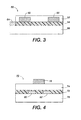
- FIG. 1 to 4 Illustrated in Figures 1 to 4 are various representative embodiments of the present disclosure, and wherein p-type semiconductors of the formulas as illustrated herein and generated, for example, from monomers containing two tertiary amines for stability primarily, and two thieno groups for extended conjugation primarily are selected as the channel or semiconductor material in thin film transistor (TFT) configurations.
- TFT thin film transistor
- p-type semiconductors of the Formulas I and II illustrated herein which are useful as microelectronic components, and which polymers possess a solubility of, for example, at least about 0.1 percent to about 95 percent by weight in common organic solvents, such as methylene chloride, tetrahydrofuran, toluene, xylene, mesitylene, chlorobenzene, dichlorobenzene, trichlorobenzene and the like, and thus these polymers can be economically fabricated by solution processes such as spin coating, screen printing, stamp printing, dip coating, solution casting, jet printing, and the like.
- solvents such as methylene chloride, tetrahydrofuran, toluene, xylene, mesitylene, chlorobenzene, dichlorobenzene, trichlorobenzene and the like
- Another feature of the present disclosure resides in providing electronic devices, such as TFTs, with p-type semiconductors of the formulas as illustrated herein as channel layer, and which layer has a conductivity of from about 10 -4 to about 10 -9 S/cm (Siemens/centimeter).
- novel p-type semiconductors of the formulas as illustrated herein and devices thereof and which devices exhibit enhanced resistance to the adverse effects of oxygen, that is, these devices exhibit relatively high current on/off ratios, and their performance does not substantially degrade as rapidly as similar devices fabricated with regioregular poly(3-alkylthiophene-3,5-diyl) or with acenes.
- a polymer and more specifically, p-type semiconductors of the formulas as illustrated herein and electronic devices thereof. More specifically, the present disclosure relates to semiconductor polymers illustrated by or encompassed by Formula (I) or by Formula (II) wherein the monomeric unit of Formula (II) is an isomer of the monomeric unit of Formula (I), wherein, for example, each R 1 through R 10 is independently hydrogen, alkyl, aryl, alkoxy, arylalkyl, alkyl substituted aryls, except that R 1 and R 2 exclude halogen, cyano, nitro and the like; a and b represent the number of rings, each of them being, for example, from 0 to about 3; and n represents the number of units, such as for example, n is a number of from about 2 to about 2,000, and more specifically, from about 2 to about 1,000, or from about 100 to about 700, or from about 2 to about 50, or mixtures of I and II, for example, from about 5 percent
- the number average molecular weight (M n ) of the polymer in embodiments can be, for example, from about 500 to about 300,000, including from about 500 to about 100,000, and the weight average molecular weight (M w ) thereof can be from about 600 to about 500,000, including from about 600 to about 200,000, both as measured by gel permeation chromatography using polystyrene standards.
- a specific class of p-type channel semiconductors are represented by the following formulas wherein each R 1 through R 6 is, for example, independently hydrogen, a suitable hydrocarbon like alkyl, aryl, alkoxy, arylalkyl, alkyl substituted aryls, and the like; and mixtures thereof; and n represents the number of units, such as for example, n is a number of from about 2 to about 5,000, and more specifically, from about 2 to about 1,000 or from about 2 to about 700.
- R 1 through R 6 are, more specifically, alkyl, arylalkyl, and alkyl substituted aryls.
- R 1 and R 2 are alkyl with about 5 to about 20 carbon atoms of, for example, pentyl, hexyl, heptyl, octyl, nonyl, decyl, undecyl, dodecyl, tridecyl, tetradecyl, pentadecyl, hexadecyl, heptadecyl or octadecyl; arylalkyl with about 7 to about 26 carbon atoms of, for example, methylphenyl (tolyl), ethylphenyl, propylphenyl, butylphenyl, pentylphenyl, hexylphenyl, heptylphenyl, octylphenyl, nonylphenyl, decylphenyl, undecylphenyl, dodecylphenyl, tridecylphenyl, t
- said semiconductor is p-type semiconductors optionally generated from monomers containing two tertiary amines and two thieno groups, and which p-type is of the following formulas wherein at least one of R 1 to R 6 is alkyl or aryl, and n is a number of from 2 to about 100.
- each R is aryl containing from 6 to about 36 carbon atoms.
- alkyl and alkoxy contain from 1 to about 25 carbon atoms, and halogen is chloride, fluoride, iodide, or bromide.
- alkyl or alkoxy contains from about 1 to about 12 carbon atoms.
- n is a number of from about 10 to about 200, or from about 20 to about 100. In a further embodiment n is about 50. In a further embodiment aryl contains from 6 to about 48 carbon atoms. In a further embodiment aryl contains from 6 to about 18 carbon atoms. In a further embodiment said semiconductor is of Formula I. In a further embodiment said semiconductor is of Formula II.
- alkyl is butyl, pentyl, hexyl, heptyl, octyl, nonyl, decyl, undecyl, dodecyl, tridecyl, tetradecyl, pentadecyl, hexadecyl, heptadecyl, octadecyl, nonadecyl, or eicosanyl.
- semiconductor is of the following alternative formulas wherein at least one of R 1 to R 6 is alkyl, aryl, or arylalkyl, and n is a number of from 2 to about 200.
- said semiconductor is of the following formulas wherein n is from 2 to about 100.
- said substrate is a plastic sheet of a polyester, a polycarbonate, or a polyimide;
- said gate source and drain electrodes are each independently comprised of silver, gold, nickel, aluminum, chromium, platinum, or indium titanium oxide, or a conductive polymer; and
- said gate dielectric layer is comprised of inorganic nitrides or oxides, or organic polymers, silicon nitride, silicon oxide.
- said semiconductor is deposited by solution processes of spin coating, stamp printing, screen printing, or jet printing.
- an electronic device comprises a semiconductive component and wherein said device is a thin film transistor, and said component is selected from the group consisting of or mixtures thereof wherein at least one of R 1 to R 10 is a suitable hydrocarbon; a and b represent the number of rings; and n represents the number of repeating units.
- said arylalkyl contains from 7 to about 37 carbon atoms.
- said R 1 to R 10 is methyl, ethyl, propyl, butyl, pentyl, hexyl, heptyl, octyl, nonyl, decyl, undecyl, dodecyl, tridecyl, tetradecyl, pentadecyl, hexadecyl, heptadecyl, octadecyl, nonadecyl, eicosanyl, hydroxymethyl, hydroxyethyl, hydroxypropyl, hydroxybutyl, hydroxypentyl, hydroxyhexyl, hydroxyheptyl, hydroxyoctyl, hydroxynonyl, hydroxydecyl, hydroxyundecyl, hydroxydodecyl, methoxyethyl, methoxypropyl, methoxybutyl, methoxypentyl, methoxyoc
- said aryl or arylalkyl is phenyl, methylphenyl, ethylphenyl, propylphenyl, butylphenyl, pentylphenyl, hexylphenyl, heptylphenyl, octylphenyl, nonylphenyl, decylphenyl, undecylphenyl, dodecylphenyl, tridecylphenyl, tetradecylphenyl, pentadecylphenyl, hexadecylphenyl, heptadecylphenyl, or octadecylphenyl.
- a is a number of from zero to about 15.
- b is a number of from zero to about 15.
- each a and b is a number of from about 1 to about 4.
- at least one of R 3 to R 10 is alkyl with from 1 to about 12 carbon atoms, alkoxy with from 1 to about 12 carbon atoms, or aryl with from 6 to about 42 carbon atoms.
- the process for the preparation of the polymer semiconductor of the formulas as illustrated herein can be accomplished by, for example, the oxidative coupling polymerization of monomer (III) in the presence of oxidative coupling agent of, for example, FeCl 3 at elevated temperatures of, for example, from room temperature to about 80°C, or by the dehalogenative coupling polymerization of monomer (lV) in the presence of zinc, nickel(II) chloride, 2,2'-dipyridil, and triphenylphosphine in dimethylacetamide (DMAc) at elevated temperatures of, for example, from about 70°C to about 90°C, and more specifically, about 80°C for a suitable period of time, like 24 hours.
- oxidative coupling agent of, for example, FeCl 3
- DMAc dimethylacetamide
- each R 1 through R 6 is as illustrated herein like hydrogen, alkyl, aryl, alkoxy, arylalkyl, alkyl substituted aryls, and the like; and mixtures thereof; and n represents the number of units, such as for example, n is a number of from about 2 to about 500, and more specifically, from about 2 to about 1,000, or from about 2 to about 700.
- each of the R groups include alkoxy and alkyl with, for example, from about 1 to about 30, including from about 4 to about 18 carbon atoms (included throughout are numbers within the range, for example 4, 5, 6, 7, 8, 9, 10, 11, 12, 13, 14, 15, 16, 17 and 18), and further including from about 6 to about 16 carbon atoms, such as methyl, ethyl, propyl, butyl, pentyl, hexyl, heptyl, octyl, nonyl, decyl, undecyl, dodecyl, tridecyl, tetradecyl, pentadecyl, hexadecyl, heptadecyl, octadecyl, nonadecyl, or eicosanyl, isomeric forms thereof, mixtures thereof, and the like, and the corresponding alkoxides, such as propoxy and butoxy; alkylaryl with
- Halogen includes chloride, bromide, fluoride and iodide.
- Heteroatoms and hetero containing groups include, for example, polyethers, trialkylsilyls, heteroaryls, and the like; and more specifically, thienyl, furyl and pyridiaryl.
- the hetero component can be selected from a number of known atoms like sulfur, oxygen, nitrogen, silicon, selenium, and the like.
- n is, for example, from about 2 to about 50.
- the polymer semiconductors are soluble or substantially soluble in common coating solvents, for example, in embodiments they possess a solubility of at least about 0.1 percent by weight, and more specifically, from about 0.5 percent to about 10 percent, or to about 95 percent by weight in such solvents as methylene chloride, 1,2-dichloroethane, tetrahydrofuran, toluene, xylene, mesitylene, chlorobenzene, dichlorobenzene, and the like.
- p-type semiconductors of the formulas as illustrated herein and generated, for example, from monomers containing two tertiary amines for stability primarily, and two thieno groups for extended conjugation of the present disclosure in embodiments when fabricated as semiconductor channel layers in TFT devices provide a stable conductivity of, for example, from about 10 -9 S/cm to about 10 -4 S/cm, and more specifically, from about 10 -8 S/cm to about 10 -5 S/cm as determined by conventional four-probe conductivity measurements.
- p-type semiconductors disclosed when fabricated from solutions as thin films of, for example, from about 10 nanometers to about 500 nanometers or from about 50 to about 300 nanometers in thickness materials are more stable in ambient conditions than similar devices fabricated from poly(3-alkylthiophene-2,5-diyl).
- the aforementioned p-type semiconductors of the formulas as illustrated herein and devices thereof are generally stable for a number of weeks rather than days or hours as is the situation with poly(3-alkylthiophene-2,5-diyl) after exposure to ambient oxygen, thus the devices fabricated from p-type semiconductors of the formulas as illustrated herein and generated, for example, from monomers containing two tertiary amines for stability primarily, and two thieno groups in embodiments of the present disclosure can provide higher current on/off ratios, and their performance characteristics do not substantially change as rapidly as poly(3-alkylthiophene-2,5-diyl) when no rigorous procedural precautions have been taken to exclude ambient oxygen during material preparation, device fabrication, and evaluation.
- P-type semiconductors disclosed are in embodiments stable, that is they do not substantially degrade when exposed to oxygen.
- an electronic device comprising a semiconductor selected from the group consisting of at least one of Formula (I), Formula (II), or mixtures thereof wherein each R 1 through R 10 is independently hydrogen, alkyl, aryl, alkoxy, halogen, arylalkyl, cyano, or nitro providing that R 1 and R 2 exclude halogen, nitro and cyano; a and b represent the number of rings; and n represents the number of repeating groups or moieties; a thin film transistor comprised of a substrate, a gate electrode, a gate dielectric layer, a source electrode and a drain electrode, and in contact with the source/drain electrodes and the gate dielectric layer a semiconductor layer comprised of at least one component or mixtures thereof of the following formulas wherein each R 1 through R 10 is independently hydrogen, alkyl, aryl, alkoxy, halogen, arylalkyl, cyano, or nitro providing that R 1 and R 2 exclude halogen, nitro
- FIG. 1 there is schematically illustrated a TFT configuration 10 comprised of a substrate 16, in contact therewith a metal contact 18 (gate electrode), and a layer of an insulating dielectric layer 14 with the gate electrode having a portion thereof or the entire gate in contact with the dielectric layer 14 on top of which layer 14 two metal contacts, 20 and 22 (source and drain electrodes), are deposited.
- a metal contact 18 gate electrode
- a layer of an insulating dielectric layer 14 with the gate electrode having a portion thereof or the entire gate in contact with the dielectric layer 14 on top of which layer 14 two metal contacts, 20 and 22 (source and drain electrodes), are deposited.
- n is 50
- the gate electrode can be included in the substrate, in the dielectric layer, and the like throughout.
- FIG. 2 schematically illustrates another TFT configuration 30 comprised of a substrate 36, a gate electrode 38, a source electrode 40, and a drain electrode 42, an insulating dielectric layer 34, and p-type semiconductor layer 32 of Formula (5) wherein n is 50.
- FIG. 3 schematically illustrates a further TFT configuration 50 comprised of a heavily n-doped silicon wafer 56, which can act as a gate electrode, a thermally grown silicon oxide dielectric layer 54, p-type semiconductor layer 52 of Formula (5) wherein n is 50, on top of which are deposited a source electrode 60 and a drain electrode 62; and a gate electrode contact 64.
- FIG. 4 schematically illustrates a TFT configuration 70 comprised of substrate 76, a gate electrode 78, a source electrode 80, a drain electrode 82, p-type semiconductors of the formulas as illustrated herein semiconductor layer 72 of Formula (5) wherein n is 50, and an insulating dielectric layer 74.
- TFT devices are envisioned, reference for example known TFT devices.
- an optional protecting layer may be incorporated on top of each of the transistor configurations of Figures 1, 2, 3 and 4.
- the insulating dielectric layer 74 may also function as a protecting layer.
- the substrate layer may generally be a silicon material inclusive of various appropriate forms of silicon, a glass plate, a plastic film or a sheet, and the like depending on the intended applications.
- a plastic substrate such as for example polyester, polycarbonate, polyimide sheets, and the like, may be selected.
- the thickness of the substrate may be, for example, from about 10 micrometers to over 10 millimeters with a specific thickness being from about 50 to about 100 micrometers, especially for a flexible plastic substrate, and from about 1 to about 10 millimeters for a rigid substrate such as glass or silicon.
- the insulating dielectric layer which can separate the gate electrode from the source and drain electrodes, and in contact with the semiconductor layer, can generally be an inorganic material film, an organic polymer film, or an organic-inorganic composite film.
- the thickness of the dielectric layer is, for example, from about 10 nanometers to about 1 micrometer with a more specific thickness being about 100 nanometers to about 500 nanometers.
- Illustrative examples of inorganic materials suitable as the dielectric layer include silicon oxide, silicon nitride, aluminum oxide, barium titanate, barium zirconate titanate, and the like; illustrative examples of organic polymers for the dielectric layer include polyesters, polycarbonates, poly(vinyl phenol), polyimides, polystyrene, poly(methacrylate)s, poly(acrylate)s, epoxy resin, and the like; and illustrative examples of inorganic-organic composite materials include nanosized metal oxide particles dispersed in polymers, such as polyester, polyimide, epoxy resin and the like.
- the insulating dielectric layer is generally of a thickness of from about 50 nanometers to about 500 nanometers depending on the dielectric constant of the dielectric material used. More specifically, the dielectric material has a dielectric constant of, for example, at least about 3, thus a suitable dielectric thickness of about 300 nanometers can provide a desirable capacitance, for example, of about 10 -9 to about 10 -7 F/cm 2 .
- the active semiconductor layer comprised of p-type semiconductors of the formulas as illustrated herein, and wherein the thickness of this layer is generally, for example, about 10 nanometers to about 1 micrometer, or about 40 to about 100 nanometers.
- This layer can generally be fabricated by solution processes such as spin coating, casting, screen, stamp, or jet printing of a solution of p-type semiconductors of the present disclosure.
- the gate electrode can be a thin metal film, a conducting polymer film, a conducting film generated from a conducting ink or paste, or the substrate itself (for example heavily doped silicon).
- gate electrode materials include, but are not limited to aluminum, gold, chromium, indium tin oxide, conducting polymers, such as polystyrene sulfonate-doped poly(3,4-ethylenedioxythiophene) (PSS/PEDOT), a conducting ink/paste comprised of carbon black/graphite or colloidal silver dispersion contained in a polymer binder, such as Electrodag available from Acheson Colloids Company, and silver filled electrically conductive thermoplastic ink available from Noelle Industries, and the like.
- the gate layer can be prepared by vacuum evaporation, sputtering of metals or conductive metal oxides, coating from conducting polymer solutions or conducting inks or dispersions by spin coating, casting or printing.
- the thickness of the gate electrode layer is, for example, from about 10 nanometers to about 10 micrometers, and a specific thickness is, for example, from about 10 to about 200 nanometers for metal films and about 1 to about 10 micrometers for polymer conductors.
- the source and drain electrode layer can be fabricated from materials which provide a low resistance ohmic contact to the semiconductor layer.
- Typical materials suitable for use as source and drain electrodes include those of the gate electrode materials such as gold, nickel, aluminum, platinum, conducting polymers, and conducting inks.
- Typical thickness of this layer is, for example, from about 40 nanometers to about 1 micrometer with the more specific thickness being about 100 to about 400 nanometers.
- the TFT devices contain a semiconductor channel with a width W and length L.
- the semiconductor channel width may be, for example, from about 10 micrometers to about 5 millimeters with a specific channel width being about 100 micrometers to about 1 millimeter.
- the semiconductor channel length may be, for example, from about 1 micrometer to about 1 millimeter with a more specific channel length being from about 5 micrometers to about 100 micrometers.
- the source electrode is grounded and a bias voltage of generally, for example, about 0 volt to about -80 volts is applied to the drain electrode to collect the charge carriers transported across the semiconductor channel when a voltage of generally, for example, about +10 volts to about -80 volts is applied to the gate electrode.
- the tertiary amine center groups function primarily to minimize or avoid instability because of exposure to oxygen and thus increase the oxidative stability of the semiconductor of the formulas as illustrated herein and generated, for example, from monomers containing two tertiary amines for stability primarily, and two thieno end groups in solution under ambient conditions and the substituents, such as alkyl, permit the solubility of these polymers in common solvents, such as ethylene chloride.
Landscapes
- Chemical & Material Sciences (AREA)
- Organic Chemistry (AREA)
- Health & Medical Sciences (AREA)
- Chemical Kinetics & Catalysis (AREA)
- Medicinal Chemistry (AREA)
- Polymers & Plastics (AREA)
- Materials Engineering (AREA)
- Engineering & Computer Science (AREA)
- Spectroscopy & Molecular Physics (AREA)
- Physics & Mathematics (AREA)
- Thin Film Transistor (AREA)
- Electroluminescent Light Sources (AREA)
- Polyoxymethylene Polymers And Polymers With Carbon-To-Carbon Bonds (AREA)
- Addition Polymer Or Copolymer, Post-Treatments, Or Chemical Modifications (AREA)
- Organic Low-Molecular-Weight Compounds And Preparation Thereof (AREA)
Applications Claiming Priority (1)
| Application Number | Priority Date | Filing Date | Title |
|---|---|---|---|
| US11/399,141 US7563860B2 (en) | 2006-04-06 | 2006-04-06 | Semiconductors and electronic devices generated therefrom |
Publications (3)
| Publication Number | Publication Date |
|---|---|
| EP1843408A2 true EP1843408A2 (fr) | 2007-10-10 |
| EP1843408A3 EP1843408A3 (fr) | 2011-09-21 |
| EP1843408B1 EP1843408B1 (fr) | 2013-09-11 |
Family
ID=38069292
Family Applications (1)
| Application Number | Title | Priority Date | Filing Date |
|---|---|---|---|
| EP07105636.0A Active EP1843408B1 (fr) | 2006-04-06 | 2007-04-04 | Semi-conducteurs et dispositifs électroniques correspondants |
Country Status (7)
| Country | Link |
|---|---|
| US (1) | US7563860B2 (fr) |
| EP (1) | EP1843408B1 (fr) |
| JP (1) | JP5192716B2 (fr) |
| KR (1) | KR101390243B1 (fr) |
| CN (1) | CN101050268B (fr) |
| CA (1) | CA2583047C (fr) |
| TW (1) | TWI456815B (fr) |
Families Citing this family (5)
| Publication number | Priority date | Publication date | Assignee | Title |
|---|---|---|---|---|
| EP1701293B1 (fr) * | 2005-03-08 | 2008-07-16 | Adalbert Gubo | Procédé de contrôler l'intégrité d'une pluralité de colis |
| US7615607B2 (en) * | 2006-04-06 | 2009-11-10 | Xerox Corporation | Semiconductor polymers |
| US20110031475A1 (en) * | 2009-08-10 | 2011-02-10 | Xerox Corporation | Semiconductor Composition |
| JP6332644B2 (ja) * | 2013-04-30 | 2018-05-30 | 国立研究開発法人理化学研究所 | 化合物、高分子化合物、有機半導体材料、有機半導体デバイス、化合物の合成方法、高分子化合物の合成方法 |
| US10074818B2 (en) * | 2013-07-23 | 2018-09-11 | Toppan Forms Co., Ltd. | Transistor |
Family Cites Families (15)
| Publication number | Priority date | Publication date | Assignee | Title |
|---|---|---|---|---|
| KR940000143B1 (ko) * | 1991-06-25 | 1994-01-07 | 재단법인 한국전자통신연구소 | 대형 박막 트랜지스터(TFT) 액정 디스플레이 패널(LCD panel)의 제조방법 |
| US5619357A (en) | 1995-06-06 | 1997-04-08 | International Business Machines Corporation | Flat panel display containing black matrix polymer |
| US5969376A (en) | 1996-08-23 | 1999-10-19 | Lucent Technologies Inc. | Organic thin film transistor having a phthalocyanine semiconductor layer |
| US6107117A (en) | 1996-12-20 | 2000-08-22 | Lucent Technologies Inc. | Method of making an organic thin film transistor |
| US5936259A (en) * | 1997-10-16 | 1999-08-10 | Lucent Technologies Inc. | Thin film transistor and organic semiconductor material thereof |
| US5777070A (en) | 1997-10-23 | 1998-07-07 | The Dow Chemical Company | Process for preparing conjugated polymers |
| DE10143353A1 (de) * | 2001-09-04 | 2003-03-20 | Covion Organic Semiconductors | Konjugierte Polymere enthaltend Spirobifluoren-Einheiten und deren Verwendung |
| US6770904B2 (en) | 2002-01-11 | 2004-08-03 | Xerox Corporation | Polythiophenes and electronic devices generated therefrom |
| US7250625B2 (en) | 2002-01-11 | 2007-07-31 | Xerox Corporation | Polythiophenes and electronic devices generated therefrom |
| CN1176477C (zh) * | 2002-03-15 | 2004-11-17 | 清华大学 | 采用凝胶聚合物电解质超电容器的制作方法 |
| US6869699B2 (en) * | 2003-03-18 | 2005-03-22 | Eastman Kodak Company | P-type materials and mixtures for electronic devices |
| US7270871B2 (en) * | 2004-01-12 | 2007-09-18 | Air Products And Chemicals, Inc. | Dispersions and films comprising conducting polymer for optoelectronic devices |
| JP2005206750A (ja) * | 2004-01-26 | 2005-08-04 | Konica Minolta Holdings Inc | 有機半導体材料、有機トランジスタ、電界効果トランジスタ、スイッチング素子及び5員複素環化合物 |
| US7615607B2 (en) * | 2006-04-06 | 2009-11-10 | Xerox Corporation | Semiconductor polymers |
| US7372071B2 (en) * | 2006-04-06 | 2008-05-13 | Xerox Corporation | Functionalized heteroacenes and electronic devices generated therefrom |
-
2006
- 2006-04-06 US US11/399,141 patent/US7563860B2/en active Active
-
2007
- 2007-03-29 CA CA2583047A patent/CA2583047C/fr active Active
- 2007-04-04 JP JP2007098065A patent/JP5192716B2/ja active Active
- 2007-04-04 TW TW096112012A patent/TWI456815B/zh active
- 2007-04-04 EP EP07105636.0A patent/EP1843408B1/fr active Active
- 2007-04-05 CN CN2007100898819A patent/CN101050268B/zh active Active
- 2007-04-06 KR KR1020070034382A patent/KR101390243B1/ko active Active
Also Published As
| Publication number | Publication date |
|---|---|
| CN101050268A (zh) | 2007-10-10 |
| JP2007277552A (ja) | 2007-10-25 |
| CA2583047A1 (fr) | 2007-10-06 |
| TWI456815B (zh) | 2014-10-11 |
| CA2583047C (fr) | 2013-03-12 |
| EP1843408B1 (fr) | 2013-09-11 |
| KR101390243B1 (ko) | 2014-04-30 |
| CN101050268B (zh) | 2012-01-11 |
| EP1843408A3 (fr) | 2011-09-21 |
| US20070235724A1 (en) | 2007-10-11 |
| TW200805724A (en) | 2008-01-16 |
| US7563860B2 (en) | 2009-07-21 |
| JP5192716B2 (ja) | 2013-05-08 |
| KR20070100181A (ko) | 2007-10-10 |
Similar Documents
| Publication | Publication Date | Title |
|---|---|---|
| EP1843410B1 (fr) | Hétéroacènes fonctionnalisés et dispositifs électroniques correspondants | |
| US20030160234A1 (en) | Polythiophenes and devices thereof | |
| US7994497B2 (en) | Poly[bis(ethynyl)heteroacene]s and electronic devices generated therefrom | |
| US7557370B2 (en) | Heteroacene polymers and electronic devices generated therefrom | |
| EP1843408B1 (fr) | Semi-conducteurs et dispositifs électroniques correspondants | |
| EP1849812B1 (fr) | Polymères d'arylamine liés et dispositifs électroniques correspondants | |
| US8049205B2 (en) | Poly(alkynylthiophene)s and electronic devices generated therefrom | |
| US7615607B2 (en) | Semiconductor polymers | |
| US7550760B2 (en) | Polyacenes and electronic devices generated therefrom | |
| US7795373B2 (en) | Ethynylene acene polymers | |
| US8334391B2 (en) | Functionalized heteroacenes | |
| US7705111B2 (en) | Poly(alkynylthiophene)s | |
| US7517476B2 (en) | Polydiazaacenes | |
| US7847052B2 (en) | Linked arylamine polymers | |
| US7517477B2 (en) | Polydiazaacenes and electronic devices generated therefrom | |
| US7586120B2 (en) | Ethynylene acene polymers and electronic devices generated therefrom |
Legal Events
| Date | Code | Title | Description |
|---|---|---|---|
| PUAI | Public reference made under article 153(3) epc to a published international application that has entered the european phase |
Free format text: ORIGINAL CODE: 0009012 |
|
| AK | Designated contracting states |
Kind code of ref document: A2 Designated state(s): AT BE BG CH CY CZ DE DK EE ES FI FR GB GR HU IE IS IT LI LT LU LV MC MT NL PL PT RO SE SI SK TR |
|
| AX | Request for extension of the european patent |
Extension state: AL BA HR MK YU |
|
| PUAL | Search report despatched |
Free format text: ORIGINAL CODE: 0009013 |
|
| AK | Designated contracting states |
Kind code of ref document: A3 Designated state(s): AT BE BG CH CY CZ DE DK EE ES FI FR GB GR HU IE IS IT LI LT LU LV MC MT NL PL PT RO SE SI SK TR |
|
| AX | Request for extension of the european patent |
Extension state: AL BA HR MK RS |
|
| RIC1 | Information provided on ipc code assigned before grant |
Ipc: H01L 51/05 20060101AFI20110812BHEP |
|
| 17P | Request for examination filed |
Effective date: 20120321 |
|
| AKX | Designation fees paid |
Designated state(s): DE FR GB |
|
| GRAP | Despatch of communication of intention to grant a patent |
Free format text: ORIGINAL CODE: EPIDOSNIGR1 |
|
| RIC1 | Information provided on ipc code assigned before grant |
Ipc: H01L 51/05 20060101AFI20130218BHEP Ipc: C08G 61/12 20060101ALI20130218BHEP |
|
| GRAS | Grant fee paid |
Free format text: ORIGINAL CODE: EPIDOSNIGR3 |
|
| GRAA | (expected) grant |
Free format text: ORIGINAL CODE: 0009210 |
|
| AK | Designated contracting states |
Kind code of ref document: B1 Designated state(s): DE FR GB |
|
| REG | Reference to a national code |
Ref country code: GB Ref legal event code: FG4D |
|
| REG | Reference to a national code |
Ref country code: DE Ref legal event code: R096 Ref document number: 602007032773 Country of ref document: DE Effective date: 20131107 |
|
| REG | Reference to a national code |
Ref country code: DE Ref legal event code: R097 Ref document number: 602007032773 Country of ref document: DE |
|
| PLBE | No opposition filed within time limit |
Free format text: ORIGINAL CODE: 0009261 |
|
| STAA | Information on the status of an ep patent application or granted ep patent |
Free format text: STATUS: NO OPPOSITION FILED WITHIN TIME LIMIT |
|
| 26N | No opposition filed |
Effective date: 20140612 |
|
| REG | Reference to a national code |
Ref country code: DE Ref legal event code: R097 Ref document number: 602007032773 Country of ref document: DE Effective date: 20140612 |
|
| REG | Reference to a national code |
Ref country code: FR Ref legal event code: PLFP Year of fee payment: 10 |
|
| REG | Reference to a national code |
Ref country code: FR Ref legal event code: PLFP Year of fee payment: 11 |
|
| REG | Reference to a national code |
Ref country code: FR Ref legal event code: PLFP Year of fee payment: 12 |
|
| REG | Reference to a national code |
Ref country code: DE Ref legal event code: R079 Ref document number: 602007032773 Country of ref document: DE Free format text: PREVIOUS MAIN CLASS: H01L0051050000 Ipc: H10K0010000000 |
|
| PGFP | Annual fee paid to national office [announced via postgrant information from national office to epo] |
Ref country code: FR Payment date: 20250319 Year of fee payment: 19 |
|
| PGFP | Annual fee paid to national office [announced via postgrant information from national office to epo] |
Ref country code: GB Payment date: 20250319 Year of fee payment: 19 |
|
| PGFP | Annual fee paid to national office [announced via postgrant information from national office to epo] |
Ref country code: DE Payment date: 20250319 Year of fee payment: 19 |