EP1843988B1 - Hinsichtlich hf-eigenschaften optimierte zusammensetzungen von (re)ba2cu3o7-d-dünnfilm-supraleitern - Google Patents
Hinsichtlich hf-eigenschaften optimierte zusammensetzungen von (re)ba2cu3o7-d-dünnfilm-supraleitern Download PDFInfo
- Publication number
- EP1843988B1 EP1843988B1 EP05855665A EP05855665A EP1843988B1 EP 1843988 B1 EP1843988 B1 EP 1843988B1 EP 05855665 A EP05855665 A EP 05855665A EP 05855665 A EP05855665 A EP 05855665A EP 1843988 B1 EP1843988 B1 EP 1843988B1
- Authority
- EP
- European Patent Office
- Prior art keywords
- films
- bco
- values
- superconducting
- properties
- Prior art date
- Legal status (The legal status is an assumption and is not a legal conclusion. Google has not performed a legal analysis and makes no representation as to the accuracy of the status listed.)
- Ceased
Links
- 239000000203 mixture Substances 0.000 title claims description 88
- 239000010409 thin film Substances 0.000 title claims description 71
- 239000002887 superconductor Substances 0.000 title description 7
- 229910052761 rare earth metal Inorganic materials 0.000 claims description 130
- 150000002910 rare earth metals Chemical class 0.000 claims description 117
- 239000000758 substrate Substances 0.000 claims description 32
- 230000007704 transition Effects 0.000 claims description 13
- 239000010408 film Substances 0.000 description 152
- 239000010949 copper Substances 0.000 description 40
- 239000000463 material Substances 0.000 description 33
- 238000005259 measurement Methods 0.000 description 28
- 150000001875 compounds Chemical class 0.000 description 25
- 229910021521 yttrium barium copper oxide Inorganic materials 0.000 description 25
- 238000000034 method Methods 0.000 description 23
- 238000012360 testing method Methods 0.000 description 21
- QRZUPJILJVGUFF-UHFFFAOYSA-N 2,8-dibenzylcyclooctan-1-one Chemical compound C1CCCCC(CC=2C=CC=CC=2)C(=O)C1CC1=CC=CC=C1 QRZUPJILJVGUFF-UHFFFAOYSA-N 0.000 description 18
- 229910052727 yttrium Inorganic materials 0.000 description 17
- VWQVUPCCIRVNHF-UHFFFAOYSA-N yttrium atom Chemical compound [Y] VWQVUPCCIRVNHF-UHFFFAOYSA-N 0.000 description 12
- 150000002500 ions Chemical class 0.000 description 11
- 238000006467 substitution reaction Methods 0.000 description 11
- QVGXLLKOCUKJST-UHFFFAOYSA-N atomic oxygen Chemical compound [O] QVGXLLKOCUKJST-UHFFFAOYSA-N 0.000 description 10
- 229910052760 oxygen Inorganic materials 0.000 description 10
- 239000001301 oxygen Substances 0.000 description 10
- 239000013078 crystal Substances 0.000 description 9
- 238000004519 manufacturing process Methods 0.000 description 9
- 238000005001 rutherford backscattering spectroscopy Methods 0.000 description 9
- 229910052788 barium Inorganic materials 0.000 description 8
- 238000000151 deposition Methods 0.000 description 8
- 239000000047 product Substances 0.000 description 8
- 229910052692 Dysprosium Inorganic materials 0.000 description 7
- 229910052691 Erbium Inorganic materials 0.000 description 7
- 150000001768 cations Chemical class 0.000 description 7
- 230000000694 effects Effects 0.000 description 7
- 239000000523 sample Substances 0.000 description 7
- 229910052689 Holmium Inorganic materials 0.000 description 6
- 125000004429 atom Chemical group 0.000 description 6
- 230000001413 cellular effect Effects 0.000 description 6
- 229910052802 copper Inorganic materials 0.000 description 6
- 230000008021 deposition Effects 0.000 description 6
- 238000009616 inductively coupled plasma Methods 0.000 description 6
- 229910002480 Cu-O Inorganic materials 0.000 description 5
- 229910052779 Neodymium Inorganic materials 0.000 description 5
- 238000001704 evaporation Methods 0.000 description 5
- 230000008020 evaporation Effects 0.000 description 5
- 229910052746 lanthanum Inorganic materials 0.000 description 5
- 230000003746 surface roughness Effects 0.000 description 5
- QPLDLSVMHZLSFG-UHFFFAOYSA-N Copper oxide Chemical compound [Cu]=O QPLDLSVMHZLSFG-UHFFFAOYSA-N 0.000 description 4
- 229910052777 Praseodymium Inorganic materials 0.000 description 4
- 239000000470 constituent Substances 0.000 description 4
- 238000005457 optimization Methods 0.000 description 4
- 239000002245 particle Substances 0.000 description 4
- 230000008569 process Effects 0.000 description 4
- 238000001228 spectrum Methods 0.000 description 4
- 239000000126 substance Substances 0.000 description 4
- IRLPACMLTUPBCL-KQYNXXCUSA-N 5'-adenylyl sulfate Chemical compound C1=NC=2C(N)=NC=NC=2N1[C@@H]1O[C@H](COP(O)(=O)OS(O)(=O)=O)[C@@H](O)[C@H]1O IRLPACMLTUPBCL-KQYNXXCUSA-N 0.000 description 3
- 229910052684 Cerium Inorganic materials 0.000 description 3
- RYGMFSIKBFXOCR-UHFFFAOYSA-N Copper Chemical compound [Cu] RYGMFSIKBFXOCR-UHFFFAOYSA-N 0.000 description 3
- 229910052693 Europium Inorganic materials 0.000 description 3
- 229910002244 LaAlO3 Inorganic materials 0.000 description 3
- PNEYBMLMFCGWSK-UHFFFAOYSA-N aluminium oxide Inorganic materials [O-2].[O-2].[O-2].[Al+3].[Al+3] PNEYBMLMFCGWSK-UHFFFAOYSA-N 0.000 description 3
- DSAJWYNOEDNPEQ-UHFFFAOYSA-N barium atom Chemical compound [Ba] DSAJWYNOEDNPEQ-UHFFFAOYSA-N 0.000 description 3
- 229910052593 corundum Inorganic materials 0.000 description 3
- 230000007547 defect Effects 0.000 description 3
- 238000013461 design Methods 0.000 description 3
- 238000010894 electron beam technology Methods 0.000 description 3
- 238000002149 energy-dispersive X-ray emission spectroscopy Methods 0.000 description 3
- 230000004907 flux Effects 0.000 description 3
- 238000002354 inductively-coupled plasma atomic emission spectroscopy Methods 0.000 description 3
- 238000003780 insertion Methods 0.000 description 3
- 230000037431 insertion Effects 0.000 description 3
- 238000012545 processing Methods 0.000 description 3
- 238000011160 research Methods 0.000 description 3
- 230000003595 spectral effect Effects 0.000 description 3
- 229910052723 transition metal Inorganic materials 0.000 description 3
- 150000003624 transition metals Chemical class 0.000 description 3
- 229910001845 yogo sapphire Inorganic materials 0.000 description 3
- IJGRMHOSHXDMSA-UHFFFAOYSA-N Atomic nitrogen Chemical compound N#N IJGRMHOSHXDMSA-UHFFFAOYSA-N 0.000 description 2
- 229910052688 Gadolinium Inorganic materials 0.000 description 2
- 229910003200 NdGaO3 Inorganic materials 0.000 description 2
- 229910052772 Samarium Inorganic materials 0.000 description 2
- 229910002370 SrTiO3 Inorganic materials 0.000 description 2
- 229910052771 Terbium Inorganic materials 0.000 description 2
- 238000002441 X-ray diffraction Methods 0.000 description 2
- DOFNLZKUGHVIMH-UQWKGHMASA-N [(8r,9s,13s,14s,17s)-17-[(1e)-cycloocten-1-yl]oxy-13-methyl-6,7,8,9,11,12,14,15,16,17-decahydrocyclopenta[a]phenanthren-3-yl] benzoate Chemical compound C([C@@H]1[C@@H](C2=CC=3)CC[C@]4([C@H]1CC[C@@H]4O\C=1CCCCCC/C=1)C)CC2=CC=3OC(=O)C1=CC=CC=C1 DOFNLZKUGHVIMH-UQWKGHMASA-N 0.000 description 2
- 238000001636 atomic emission spectroscopy Methods 0.000 description 2
- 230000005540 biological transmission Effects 0.000 description 2
- 229910052791 calcium Inorganic materials 0.000 description 2
- 238000012512 characterization method Methods 0.000 description 2
- 238000010586 diagram Methods 0.000 description 2
- KBQHZAAAGSGFKK-UHFFFAOYSA-N dysprosium atom Chemical group [Dy] KBQHZAAAGSGFKK-UHFFFAOYSA-N 0.000 description 2
- 238000011065 in-situ storage Methods 0.000 description 2
- 229910052747 lanthanoid Inorganic materials 0.000 description 2
- 150000002602 lanthanoids Chemical class 0.000 description 2
- FZLIPJUXYLNCLC-UHFFFAOYSA-N lanthanum atom Chemical compound [La] FZLIPJUXYLNCLC-UHFFFAOYSA-N 0.000 description 2
- 238000000691 measurement method Methods 0.000 description 2
- 230000003647 oxidation Effects 0.000 description 2
- 238000007254 oxidation reaction Methods 0.000 description 2
- 125000004430 oxygen atom Chemical group O* 0.000 description 2
- 238000000059 patterning Methods 0.000 description 2
- 230000000737 periodic effect Effects 0.000 description 2
- 230000004044 response Effects 0.000 description 2
- 229910052706 scandium Inorganic materials 0.000 description 2
- 230000035945 sensitivity Effects 0.000 description 2
- 239000007787 solid Substances 0.000 description 2
- 241000894007 species Species 0.000 description 2
- 229910052712 strontium Inorganic materials 0.000 description 2
- ZSLUVFAKFWKJRC-IGMARMGPSA-N 232Th Chemical compound [232Th] ZSLUVFAKFWKJRC-IGMARMGPSA-N 0.000 description 1
- 239000005751 Copper oxide Substances 0.000 description 1
- VMQMZMRVKUZKQL-UHFFFAOYSA-N Cu+ Chemical compound [Cu+] VMQMZMRVKUZKQL-UHFFFAOYSA-N 0.000 description 1
- 229910052765 Lutetium Inorganic materials 0.000 description 1
- 229910052773 Promethium Inorganic materials 0.000 description 1
- 229910052776 Thorium Inorganic materials 0.000 description 1
- 229910052775 Thulium Inorganic materials 0.000 description 1
- 229910009203 Y-Ba-Cu-O Inorganic materials 0.000 description 1
- 229910003097 YBa2Cu3O7−δ Inorganic materials 0.000 description 1
- 229910052769 Ytterbium Inorganic materials 0.000 description 1
- 238000010521 absorption reaction Methods 0.000 description 1
- 239000003929 acidic solution Substances 0.000 description 1
- 229910052768 actinide Inorganic materials 0.000 description 1
- 150000001255 actinides Chemical class 0.000 description 1
- 230000002411 adverse Effects 0.000 description 1
- 238000004458 analytical method Methods 0.000 description 1
- 239000007864 aqueous solution Substances 0.000 description 1
- 238000000089 atomic force micrograph Methods 0.000 description 1
- 238000004630 atomic force microscopy Methods 0.000 description 1
- 230000015572 biosynthetic process Effects 0.000 description 1
- 230000015556 catabolic process Effects 0.000 description 1
- 238000005341 cation exchange Methods 0.000 description 1
- 230000010267 cellular communication Effects 0.000 description 1
- 229910010293 ceramic material Inorganic materials 0.000 description 1
- ZMIGMASIKSOYAM-UHFFFAOYSA-N cerium Chemical compound [Ce][Ce][Ce][Ce][Ce][Ce][Ce][Ce][Ce][Ce][Ce][Ce][Ce][Ce][Ce][Ce][Ce][Ce][Ce][Ce][Ce][Ce][Ce][Ce][Ce][Ce][Ce][Ce][Ce][Ce][Ce][Ce][Ce][Ce][Ce][Ce][Ce][Ce] ZMIGMASIKSOYAM-UHFFFAOYSA-N 0.000 description 1
- 230000008859 change Effects 0.000 description 1
- 230000005493 condensed matter Effects 0.000 description 1
- 239000004020 conductor Substances 0.000 description 1
- 229910000431 copper oxide Inorganic materials 0.000 description 1
- 238000005336 cracking Methods 0.000 description 1
- 238000002425 crystallisation Methods 0.000 description 1
- 230000008025 crystallization Effects 0.000 description 1
- 230000003247 decreasing effect Effects 0.000 description 1
- 238000006731 degradation reaction Methods 0.000 description 1
- 230000002939 deleterious effect Effects 0.000 description 1
- 238000001514 detection method Methods 0.000 description 1
- 238000009792 diffusion process Methods 0.000 description 1
- 238000009826 distribution Methods 0.000 description 1
- 230000005672 electromagnetic field Effects 0.000 description 1
- 238000000407 epitaxy Methods 0.000 description 1
- UYAHIZSMUZPPFV-UHFFFAOYSA-N erbium Chemical compound [Er] UYAHIZSMUZPPFV-UHFFFAOYSA-N 0.000 description 1
- OGPBJKLSAFTDLK-UHFFFAOYSA-N europium atom Chemical compound [Eu] OGPBJKLSAFTDLK-UHFFFAOYSA-N 0.000 description 1
- 238000011156 evaluation Methods 0.000 description 1
- 230000001747 exhibiting effect Effects 0.000 description 1
- 238000000605 extraction Methods 0.000 description 1
- UIWYJDYFSGRHKR-UHFFFAOYSA-N gadolinium atom Chemical compound [Gd] UIWYJDYFSGRHKR-UHFFFAOYSA-N 0.000 description 1
- KJZYNXUDTRRSPN-UHFFFAOYSA-N holmium atom Chemical compound [Ho] KJZYNXUDTRRSPN-UHFFFAOYSA-N 0.000 description 1
- 229910052500 inorganic mineral Inorganic materials 0.000 description 1
- 239000012212 insulator Substances 0.000 description 1
- 238000011835 investigation Methods 0.000 description 1
- 238000002955 isolation Methods 0.000 description 1
- 239000007788 liquid Substances 0.000 description 1
- OHSVLFRHMCKCQY-UHFFFAOYSA-N lutetium atom Chemical compound [Lu] OHSVLFRHMCKCQY-UHFFFAOYSA-N 0.000 description 1
- CPLXHLVBOLITMK-UHFFFAOYSA-N magnesium oxide Inorganic materials [Mg]=O CPLXHLVBOLITMK-UHFFFAOYSA-N 0.000 description 1
- 239000000155 melt Substances 0.000 description 1
- 239000011707 mineral Substances 0.000 description 1
- 238000002156 mixing Methods 0.000 description 1
- 238000012986 modification Methods 0.000 description 1
- 230000004048 modification Effects 0.000 description 1
- QEFYFXOXNSNQGX-UHFFFAOYSA-N neodymium atom Chemical compound [Nd] QEFYFXOXNSNQGX-UHFFFAOYSA-N 0.000 description 1
- 229910052759 nickel Inorganic materials 0.000 description 1
- 229910052757 nitrogen Inorganic materials 0.000 description 1
- 230000009022 nonlinear effect Effects 0.000 description 1
- 230000003287 optical effect Effects 0.000 description 1
- 230000000704 physical effect Effects 0.000 description 1
- PUDIUYLPXJFUGB-UHFFFAOYSA-N praseodymium atom Chemical compound [Pr] PUDIUYLPXJFUGB-UHFFFAOYSA-N 0.000 description 1
- 239000002244 precipitate Substances 0.000 description 1
- 238000001314 profilometry Methods 0.000 description 1
- VQMWBBYLQSCNPO-UHFFFAOYSA-N promethium atom Chemical compound [Pm] VQMWBBYLQSCNPO-UHFFFAOYSA-N 0.000 description 1
- 239000010453 quartz Substances 0.000 description 1
- 238000003380 quartz crystal microbalance Methods 0.000 description 1
- -1 rare earth ion Chemical class 0.000 description 1
- 229910001404 rare earth metal oxide Inorganic materials 0.000 description 1
- 230000009467 reduction Effects 0.000 description 1
- KZUNJOHGWZRPMI-UHFFFAOYSA-N samarium atom Chemical compound [Sm] KZUNJOHGWZRPMI-UHFFFAOYSA-N 0.000 description 1
- SIXSYDAISGFNSX-UHFFFAOYSA-N scandium atom Chemical compound [Sc] SIXSYDAISGFNSX-UHFFFAOYSA-N 0.000 description 1
- 238000004626 scanning electron microscopy Methods 0.000 description 1
- VYPSYNLAJGMNEJ-UHFFFAOYSA-N silicon dioxide Inorganic materials O=[Si]=O VYPSYNLAJGMNEJ-UHFFFAOYSA-N 0.000 description 1
- 239000000243 solution Substances 0.000 description 1
- 238000004611 spectroscopical analysis Methods 0.000 description 1
- 238000000992 sputter etching Methods 0.000 description 1
- 238000004381 surface treatment Methods 0.000 description 1
- GZCRRIHWUXGPOV-UHFFFAOYSA-N terbium atom Chemical compound [Tb] GZCRRIHWUXGPOV-UHFFFAOYSA-N 0.000 description 1
- 238000005382 thermal cycling Methods 0.000 description 1
- 238000012546 transfer Methods 0.000 description 1
- NAWDYIZEMPQZHO-UHFFFAOYSA-N ytterbium Chemical compound [Yb] NAWDYIZEMPQZHO-UHFFFAOYSA-N 0.000 description 1
- 229910052725 zinc Inorganic materials 0.000 description 1
Images













Classifications
-
- H—ELECTRICITY
- H10—SEMICONDUCTOR DEVICES; ELECTRIC SOLID-STATE DEVICES NOT OTHERWISE PROVIDED FOR
- H10N—ELECTRIC SOLID-STATE DEVICES NOT OTHERWISE PROVIDED FOR
- H10N60/00—Superconducting devices
- H10N60/20—Permanent superconducting devices
- H10N60/203—Permanent superconducting devices comprising high-Tc ceramic materials
-
- C—CHEMISTRY; METALLURGY
- C04—CEMENTS; CONCRETE; ARTIFICIAL STONE; CERAMICS; REFRACTORIES
- C04B—LIME, MAGNESIA; SLAG; CEMENTS; COMPOSITIONS THEREOF, e.g. MORTARS, CONCRETE OR LIKE BUILDING MATERIALS; ARTIFICIAL STONE; CERAMICS; REFRACTORIES; TREATMENT OF NATURAL STONE
- C04B35/00—Shaped ceramic products characterised by their composition; Ceramics compositions; Processing powders of inorganic compounds preparatory to the manufacturing of ceramic products
- C04B35/01—Shaped ceramic products characterised by their composition; Ceramics compositions; Processing powders of inorganic compounds preparatory to the manufacturing of ceramic products based on oxide ceramics
- C04B35/45—Shaped ceramic products characterised by their composition; Ceramics compositions; Processing powders of inorganic compounds preparatory to the manufacturing of ceramic products based on oxide ceramics based on copper oxide or solid solutions thereof with other oxides
- C04B35/4504—Shaped ceramic products characterised by their composition; Ceramics compositions; Processing powders of inorganic compounds preparatory to the manufacturing of ceramic products based on oxide ceramics based on copper oxide or solid solutions thereof with other oxides containing rare earth oxides
- C04B35/4508—Type 1-2-3
-
- H—ELECTRICITY
- H01—ELECTRIC ELEMENTS
- H01B—CABLES; CONDUCTORS; INSULATORS; SELECTION OF MATERIALS FOR THEIR CONDUCTIVE, INSULATING OR DIELECTRIC PROPERTIES
- H01B1/00—Conductors or conductive bodies characterised by the conductive materials; Selection of materials as conductors
- H01B1/06—Conductors or conductive bodies characterised by the conductive materials; Selection of materials as conductors mainly consisting of other non-metallic substances
- H01B1/08—Conductors or conductive bodies characterised by the conductive materials; Selection of materials as conductors mainly consisting of other non-metallic substances oxides
-
- H—ELECTRICITY
- H01—ELECTRIC ELEMENTS
- H01B—CABLES; CONDUCTORS; INSULATORS; SELECTION OF MATERIALS FOR THEIR CONDUCTIVE, INSULATING OR DIELECTRIC PROPERTIES
- H01B12/00—Superconductive or hyperconductive conductors, cables, or transmission lines
-
- H—ELECTRICITY
- H01—ELECTRIC ELEMENTS
- H01F—MAGNETS; INDUCTANCES; TRANSFORMERS; SELECTION OF MATERIALS FOR THEIR MAGNETIC PROPERTIES
- H01F6/00—Superconducting magnets; Superconducting coils
-
- H—ELECTRICITY
- H01—ELECTRIC ELEMENTS
- H01P—WAVEGUIDES; RESONATORS, LINES, OR OTHER DEVICES OF THE WAVEGUIDE TYPE
- H01P1/00—Auxiliary devices
- H01P1/20—Frequency-selective devices, e.g. filters
- H01P1/201—Filters for transverse electromagnetic waves
- H01P1/203—Strip line filters
- H01P1/20327—Electromagnetic interstage coupling
- H01P1/20336—Comb or interdigital filters
-
- H—ELECTRICITY
- H01—ELECTRIC ELEMENTS
- H01P—WAVEGUIDES; RESONATORS, LINES, OR OTHER DEVICES OF THE WAVEGUIDE TYPE
- H01P1/00—Auxiliary devices
- H01P1/20—Frequency-selective devices, e.g. filters
- H01P1/201—Filters for transverse electromagnetic waves
- H01P1/203—Strip line filters
- H01P1/20327—Electromagnetic interstage coupling
- H01P1/20354—Non-comb or non-interdigital filters
- H01P1/20381—Special shape resonators
-
- H—ELECTRICITY
- H10—SEMICONDUCTOR DEVICES; ELECTRIC SOLID-STATE DEVICES NOT OTHERWISE PROVIDED FOR
- H10N—ELECTRIC SOLID-STATE DEVICES NOT OTHERWISE PROVIDED FOR
- H10N60/00—Superconducting devices
-
- H—ELECTRICITY
- H10—SEMICONDUCTOR DEVICES; ELECTRIC SOLID-STATE DEVICES NOT OTHERWISE PROVIDED FOR
- H10N—ELECTRIC SOLID-STATE DEVICES NOT OTHERWISE PROVIDED FOR
- H10N60/00—Superconducting devices
- H10N60/01—Manufacture or treatment
- H10N60/0268—Manufacture or treatment of devices comprising copper oxide
- H10N60/0296—Processes for depositing or forming copper oxide superconductor layers
- H10N60/0381—Processes for depositing or forming copper oxide superconductor layers by evaporation, e.g. MBE
-
- H—ELECTRICITY
- H10—SEMICONDUCTOR DEVICES; ELECTRIC SOLID-STATE DEVICES NOT OTHERWISE PROVIDED FOR
- H10N—ELECTRIC SOLID-STATE DEVICES NOT OTHERWISE PROVIDED FOR
- H10N60/00—Superconducting devices
- H10N60/01—Manufacture or treatment
- H10N60/0268—Manufacture or treatment of devices comprising copper oxide
- H10N60/0296—Processes for depositing or forming copper oxide superconductor layers
- H10N60/0436—Processes for depositing or forming copper oxide superconductor layers by chemical vapour deposition [CVD]
-
- H—ELECTRICITY
- H10—SEMICONDUCTOR DEVICES; ELECTRIC SOLID-STATE DEVICES NOT OTHERWISE PROVIDED FOR
- H10N—ELECTRIC SOLID-STATE DEVICES NOT OTHERWISE PROVIDED FOR
- H10N60/00—Superconducting devices
- H10N60/01—Manufacture or treatment
- H10N60/0268—Manufacture or treatment of devices comprising copper oxide
- H10N60/0296—Processes for depositing or forming copper oxide superconductor layers
- H10N60/0576—Processes for depositing or forming copper oxide superconductor layers characterised by the substrate
-
- H—ELECTRICITY
- H10—SEMICONDUCTOR DEVICES; ELECTRIC SOLID-STATE DEVICES NOT OTHERWISE PROVIDED FOR
- H10N—ELECTRIC SOLID-STATE DEVICES NOT OTHERWISE PROVIDED FOR
- H10N60/00—Superconducting devices
- H10N60/01—Manufacture or treatment
- H10N60/0268—Manufacture or treatment of devices comprising copper oxide
- H10N60/0296—Processes for depositing or forming copper oxide superconductor layers
- H10N60/0576—Processes for depositing or forming copper oxide superconductor layers characterised by the substrate
- H10N60/0604—Monocrystalline substrates, e.g. epitaxial growth
-
- H—ELECTRICITY
- H10—SEMICONDUCTOR DEVICES; ELECTRIC SOLID-STATE DEVICES NOT OTHERWISE PROVIDED FOR
- H10N—ELECTRIC SOLID-STATE DEVICES NOT OTHERWISE PROVIDED FOR
- H10N60/00—Superconducting devices
- H10N60/01—Manufacture or treatment
- H10N60/0268—Manufacture or treatment of devices comprising copper oxide
- H10N60/0296—Processes for depositing or forming copper oxide superconductor layers
- H10N60/0576—Processes for depositing or forming copper oxide superconductor layers characterised by the substrate
- H10N60/0632—Intermediate layers, e.g. for growth control
-
- H—ELECTRICITY
- H10—SEMICONDUCTOR DEVICES; ELECTRIC SOLID-STATE DEVICES NOT OTHERWISE PROVIDED FOR
- H10N—ELECTRIC SOLID-STATE DEVICES NOT OTHERWISE PROVIDED FOR
- H10N60/00—Superconducting devices
- H10N60/80—Constructional details
- H10N60/85—Superconducting active materials
- H10N60/855—Ceramic superconductors
- H10N60/857—Ceramic superconductors comprising copper oxide
-
- H—ELECTRICITY
- H10—SEMICONDUCTOR DEVICES; ELECTRIC SOLID-STATE DEVICES NOT OTHERWISE PROVIDED FOR
- H10N—ELECTRIC SOLID-STATE DEVICES NOT OTHERWISE PROVIDED FOR
- H10N60/00—Superconducting devices
- H10N60/80—Constructional details
- H10N60/85—Superconducting active materials
- H10N60/855—Ceramic superconductors
- H10N60/857—Ceramic superconductors comprising copper oxide
- H10N60/858—Ceramic superconductors comprising copper oxide having multilayered structures, e.g. superlattices
-
- C—CHEMISTRY; METALLURGY
- C04—CEMENTS; CONCRETE; ARTIFICIAL STONE; CERAMICS; REFRACTORIES
- C04B—LIME, MAGNESIA; SLAG; CEMENTS; COMPOSITIONS THEREOF, e.g. MORTARS, CONCRETE OR LIKE BUILDING MATERIALS; ARTIFICIAL STONE; CERAMICS; REFRACTORIES; TREATMENT OF NATURAL STONE
- C04B2235/00—Aspects relating to ceramic starting mixtures or sintered ceramic products
- C04B2235/02—Composition of constituents of the starting material or of secondary phases of the final product
- C04B2235/30—Constituents and secondary phases not being of a fibrous nature
- C04B2235/32—Metal oxides, mixed metal oxides, or oxide-forming salts thereof, e.g. carbonates, nitrates, (oxy)hydroxides, chlorides
- C04B2235/3205—Alkaline earth oxides or oxide forming salts thereof, e.g. beryllium oxide
- C04B2235/3215—Barium oxides or oxide-forming salts thereof
-
- C—CHEMISTRY; METALLURGY
- C04—CEMENTS; CONCRETE; ARTIFICIAL STONE; CERAMICS; REFRACTORIES
- C04B—LIME, MAGNESIA; SLAG; CEMENTS; COMPOSITIONS THEREOF, e.g. MORTARS, CONCRETE OR LIKE BUILDING MATERIALS; ARTIFICIAL STONE; CERAMICS; REFRACTORIES; TREATMENT OF NATURAL STONE
- C04B2235/00—Aspects relating to ceramic starting mixtures or sintered ceramic products
- C04B2235/02—Composition of constituents of the starting material or of secondary phases of the final product
- C04B2235/30—Constituents and secondary phases not being of a fibrous nature
- C04B2235/32—Metal oxides, mixed metal oxides, or oxide-forming salts thereof, e.g. carbonates, nitrates, (oxy)hydroxides, chlorides
- C04B2235/3224—Rare earth oxide or oxide forming salts thereof, e.g. scandium oxide
-
- C—CHEMISTRY; METALLURGY
- C04—CEMENTS; CONCRETE; ARTIFICIAL STONE; CERAMICS; REFRACTORIES
- C04B—LIME, MAGNESIA; SLAG; CEMENTS; COMPOSITIONS THEREOF, e.g. MORTARS, CONCRETE OR LIKE BUILDING MATERIALS; ARTIFICIAL STONE; CERAMICS; REFRACTORIES; TREATMENT OF NATURAL STONE
- C04B2235/00—Aspects relating to ceramic starting mixtures or sintered ceramic products
- C04B2235/70—Aspects relating to sintered or melt-casted ceramic products
- C04B2235/80—Phases present in the sintered or melt-cast ceramic products other than the main phase
- C04B2235/85—Intergranular or grain boundary phases
-
- C—CHEMISTRY; METALLURGY
- C04—CEMENTS; CONCRETE; ARTIFICIAL STONE; CERAMICS; REFRACTORIES
- C04B—LIME, MAGNESIA; SLAG; CEMENTS; COMPOSITIONS THEREOF, e.g. MORTARS, CONCRETE OR LIKE BUILDING MATERIALS; ARTIFICIAL STONE; CERAMICS; REFRACTORIES; TREATMENT OF NATURAL STONE
- C04B2235/00—Aspects relating to ceramic starting mixtures or sintered ceramic products
- C04B2235/70—Aspects relating to sintered or melt-casted ceramic products
- C04B2235/96—Properties of ceramic products, e.g. mechanical properties such as strength, toughness, wear resistance
-
- Y—GENERAL TAGGING OF NEW TECHNOLOGICAL DEVELOPMENTS; GENERAL TAGGING OF CROSS-SECTIONAL TECHNOLOGIES SPANNING OVER SEVERAL SECTIONS OF THE IPC; TECHNICAL SUBJECTS COVERED BY FORMER USPC CROSS-REFERENCE ART COLLECTIONS [XRACs] AND DIGESTS
- Y10—TECHNICAL SUBJECTS COVERED BY FORMER USPC
- Y10S—TECHNICAL SUBJECTS COVERED BY FORMER USPC CROSS-REFERENCE ART COLLECTIONS [XRACs] AND DIGESTS
- Y10S505/00—Superconductor technology: apparatus, material, process
- Y10S505/775—High tc, above 30 k, superconducting material
- Y10S505/776—Containing transition metal oxide with rare earth or alkaline earth
-
- Y—GENERAL TAGGING OF NEW TECHNOLOGICAL DEVELOPMENTS; GENERAL TAGGING OF CROSS-SECTIONAL TECHNOLOGIES SPANNING OVER SEVERAL SECTIONS OF THE IPC; TECHNICAL SUBJECTS COVERED BY FORMER USPC CROSS-REFERENCE ART COLLECTIONS [XRACs] AND DIGESTS
- Y10—TECHNICAL SUBJECTS COVERED BY FORMER USPC
- Y10S—TECHNICAL SUBJECTS COVERED BY FORMER USPC CROSS-REFERENCE ART COLLECTIONS [XRACs] AND DIGESTS
- Y10S505/00—Superconductor technology: apparatus, material, process
- Y10S505/775—High tc, above 30 k, superconducting material
- Y10S505/776—Containing transition metal oxide with rare earth or alkaline earth
- Y10S505/777—Lanthanum, e.g. La2CuO4
-
- Y—GENERAL TAGGING OF NEW TECHNOLOGICAL DEVELOPMENTS; GENERAL TAGGING OF CROSS-SECTIONAL TECHNOLOGIES SPANNING OVER SEVERAL SECTIONS OF THE IPC; TECHNICAL SUBJECTS COVERED BY FORMER USPC CROSS-REFERENCE ART COLLECTIONS [XRACs] AND DIGESTS
- Y10—TECHNICAL SUBJECTS COVERED BY FORMER USPC
- Y10S—TECHNICAL SUBJECTS COVERED BY FORMER USPC CROSS-REFERENCE ART COLLECTIONS [XRACs] AND DIGESTS
- Y10S505/00—Superconductor technology: apparatus, material, process
- Y10S505/775—High tc, above 30 k, superconducting material
- Y10S505/776—Containing transition metal oxide with rare earth or alkaline earth
- Y10S505/777—Lanthanum, e.g. La2CuO4
- Y10S505/778—Alkaline earth, i.e. Ca, Sr, Ba, Ra
-
- Y—GENERAL TAGGING OF NEW TECHNOLOGICAL DEVELOPMENTS; GENERAL TAGGING OF CROSS-SECTIONAL TECHNOLOGIES SPANNING OVER SEVERAL SECTIONS OF THE IPC; TECHNICAL SUBJECTS COVERED BY FORMER USPC CROSS-REFERENCE ART COLLECTIONS [XRACs] AND DIGESTS
- Y10—TECHNICAL SUBJECTS COVERED BY FORMER USPC
- Y10S—TECHNICAL SUBJECTS COVERED BY FORMER USPC CROSS-REFERENCE ART COLLECTIONS [XRACs] AND DIGESTS
- Y10S505/00—Superconductor technology: apparatus, material, process
- Y10S505/775—High tc, above 30 k, superconducting material
- Y10S505/776—Containing transition metal oxide with rare earth or alkaline earth
- Y10S505/779—Other rare earth, i.e. Sc,Y,Ce,Pr,Nd,Pm,Sm,Eu,Gd,Tb,Dy,Ho,Er,Tm,Yb,Lu and alkaline earth, i.e. Ca,Sr,Ba,Ra
-
- Y—GENERAL TAGGING OF NEW TECHNOLOGICAL DEVELOPMENTS; GENERAL TAGGING OF CROSS-SECTIONAL TECHNOLOGIES SPANNING OVER SEVERAL SECTIONS OF THE IPC; TECHNICAL SUBJECTS COVERED BY FORMER USPC CROSS-REFERENCE ART COLLECTIONS [XRACs] AND DIGESTS
- Y10—TECHNICAL SUBJECTS COVERED BY FORMER USPC
- Y10S—TECHNICAL SUBJECTS COVERED BY FORMER USPC CROSS-REFERENCE ART COLLECTIONS [XRACs] AND DIGESTS
- Y10S505/00—Superconductor technology: apparatus, material, process
- Y10S505/775—High tc, above 30 k, superconducting material
- Y10S505/776—Containing transition metal oxide with rare earth or alkaline earth
- Y10S505/779—Other rare earth, i.e. Sc,Y,Ce,Pr,Nd,Pm,Sm,Eu,Gd,Tb,Dy,Ho,Er,Tm,Yb,Lu and alkaline earth, i.e. Ca,Sr,Ba,Ra
- Y10S505/78—Yttrium and barium-, e.g. YBa2Cu307
-
- Y—GENERAL TAGGING OF NEW TECHNOLOGICAL DEVELOPMENTS; GENERAL TAGGING OF CROSS-SECTIONAL TECHNOLOGIES SPANNING OVER SEVERAL SECTIONS OF THE IPC; TECHNICAL SUBJECTS COVERED BY FORMER USPC CROSS-REFERENCE ART COLLECTIONS [XRACs] AND DIGESTS
- Y10—TECHNICAL SUBJECTS COVERED BY FORMER USPC
- Y10T—TECHNICAL SUBJECTS COVERED BY FORMER US CLASSIFICATION
- Y10T428/00—Stock material or miscellaneous articles
- Y10T428/24—Structurally defined web or sheet [e.g., overall dimension, etc.]
- Y10T428/24355—Continuous and nonuniform or irregular surface on layer or component [e.g., roofing, etc.]
-
- Y—GENERAL TAGGING OF NEW TECHNOLOGICAL DEVELOPMENTS; GENERAL TAGGING OF CROSS-SECTIONAL TECHNOLOGIES SPANNING OVER SEVERAL SECTIONS OF THE IPC; TECHNICAL SUBJECTS COVERED BY FORMER USPC CROSS-REFERENCE ART COLLECTIONS [XRACs] AND DIGESTS
- Y10—TECHNICAL SUBJECTS COVERED BY FORMER USPC
- Y10T—TECHNICAL SUBJECTS COVERED BY FORMER US CLASSIFICATION
- Y10T428/00—Stock material or miscellaneous articles
- Y10T428/24—Structurally defined web or sheet [e.g., overall dimension, etc.]
- Y10T428/24942—Structurally defined web or sheet [e.g., overall dimension, etc.] including components having same physical characteristic in differing degree
-
- Y—GENERAL TAGGING OF NEW TECHNOLOGICAL DEVELOPMENTS; GENERAL TAGGING OF CROSS-SECTIONAL TECHNOLOGIES SPANNING OVER SEVERAL SECTIONS OF THE IPC; TECHNICAL SUBJECTS COVERED BY FORMER USPC CROSS-REFERENCE ART COLLECTIONS [XRACs] AND DIGESTS
- Y10—TECHNICAL SUBJECTS COVERED BY FORMER USPC
- Y10T—TECHNICAL SUBJECTS COVERED BY FORMER US CLASSIFICATION
- Y10T428/00—Stock material or miscellaneous articles
- Y10T428/26—Web or sheet containing structurally defined element or component, the element or component having a specified physical dimension
-
- Y—GENERAL TAGGING OF NEW TECHNOLOGICAL DEVELOPMENTS; GENERAL TAGGING OF CROSS-SECTIONAL TECHNOLOGIES SPANNING OVER SEVERAL SECTIONS OF THE IPC; TECHNICAL SUBJECTS COVERED BY FORMER USPC CROSS-REFERENCE ART COLLECTIONS [XRACs] AND DIGESTS
- Y10—TECHNICAL SUBJECTS COVERED BY FORMER USPC
- Y10T—TECHNICAL SUBJECTS COVERED BY FORMER US CLASSIFICATION
- Y10T428/00—Stock material or miscellaneous articles
- Y10T428/26—Web or sheet containing structurally defined element or component, the element or component having a specified physical dimension
- Y10T428/266—Web or sheet containing structurally defined element or component, the element or component having a specified physical dimension of base or substrate
Definitions
- This invention relates to thin films of high temperature superconducting compositions optimized for RF applications and a method for manufacturing them, more specifically rare earth compositions of (RE)Ba 2 Cu 3 O 7- ⁇ deviating significantly from the 1:2:3 stoichiometry.
- B. Batlogg first discovered and isolated the single crystallographic phase responsible for the superconducting properties of the YBCO compound. ( B.Batlogg, U.S Patent No 6,636,603 ). In isolating this single perovskite phase of a composition, Batlogg admonished that the composition was essential to isolation of the phase and that it must be within 10% of the M 2 M'Cu 3 O 7- ⁇ composition where M is a divalent cation preferably barium and M' is a trivalent cation preferably yttrium.
- compositions of these (RE)BCO compounds may be altered substantially from the nominal 1:2:3 stoichiometry in order to optimize their properties for specific applications. It is the primary object of this invention to provide high temperature superconducting thin films that have the lowest possible RF surface resistance ( R s ) values as well as the lowest achievable RF nonlinearities. This often requires fabrication of (RE)BCO films that deviate significantly from the 1:2:3 composition. It is another object of this invention to provide a thin film superconductor that is optimized for RF/microwave applications. It is another object of this invention that the film has a low surface resistance. It is another object of this invention that the film has a highly linear RF/microwave surface reactance.
- the stoichiometry of the film deviates by at least 10% from the standard 1:2:3 stoichiometry and with full substitution for yttrium by a rare earth element.
- the following films are described in US5863869 : Y 0.75 Ba 1.35 Cu 3 O 7.7 and Y 0.87 Ba 1.58 Cu 3 O 9-y , where y is sufficient to satisfy valence demands of the composition. Both of these films experienced an onset of superconductivity at about 97°K.
- EP0710992 describes a superconducting film having the following composition: Nd 1+x Ba 2-x Cu 3 0 7-d where 0.03 ⁇ x ⁇ 0.12 and 0 ⁇ d ⁇ 0.5.
- the films of this invention are high temperature superconducting (HTS) thin films specifically optimized for microwave and RF applications.
- RE a rare earth element, preferably yttrium
- This 1:2:3 stoichiometry has since been the focus of much study including varying the rare earth element, full and partial substitutions for RE, for Ba, and for Cu, oxygen doping, and deviations from the 1:2:3 stoichiometry.
- the present invention focuses on RE HTS films specifically optimized for microwave and RF applications.
- the RF/microwave HTS applications require the HTS thin films to have superior microwave properties, specifically low surface resistance, R s , and highly linear surface reactance, X s , i.e. high J IMD .
- the invention is characterized in terms of its physical composition, surface morphology, superconducting properties, and performance characteristics of microwave circuits made from these films
- this invention focuses on compositions having a significant deviation from the 1:2:3 stoichiometry in order to create the films optimized for microwave/RF applications.
- These films have a RE:Ba ratio of less than 1.8, which deviates more than 10% from the typical ratio of 2, and preferably less than 1.7.
- the research has shown that the highest quality factor values, Q , representing the surface resistance of patterned films, peak at a particular Ba:RE ratio for each RE and that these ratios deviate significantly from the 1:2:3 stoichiometry.
- the films have a superconducting transition temperature greater than 87U.
- the performance characteristics of the HTS films naturally affect their efficacy in RF/microwave HTS applications. Specifically desirable are low surface resistance, R s , ( ⁇ 15 micro-ohms at 1.85 GHz and 77 K) and highly linear surface reactance, X s , i.e., high J IMD values (>10 7 A/cm 2 , preferably >5 ⁇ 10 7 A/cm 2 at 77 K).
- HTS thin films with such properties permit the fabrication of extremely selective filters (60-dB rejection within 0.2% relative frequency, to 100-dB rejection within 0.02% relative frequency, with extremely low in-band insertion loss ( ⁇ 1-dB, preferably ⁇ 0.2-dB) in an extremely small size ( ⁇ 10-cm 2 filter chips), which can handle the interference power levels experienced at the front end of a cellular telephone base station receiver (-50 dBm to -28 dBm, to as high as -12 dBm to 0 dBm or possibly even higher) without producing undesirable distortion in the passband, particularly intermodulation distortion, and more particularly intermodulation distortion products comparable to background noise levels (-173.8 dBm/Hz).
- the films of this invention are also characterized by their optimized microwave and RF properties.
- Fig. 1 shows ⁇ -2 ⁇ x-ray diffraction scans for several (RE)BCO thin films grown on MgO substrates.
- Fig. 2 displays the 2 ⁇ (005) x-ray peak positions as a function of the Ba/RE ratio for different compositions of the various (RE)BCO thin films indicated.
- Fig. 3 displays the 2 ⁇ (005) x-ray peak intensities as a function of the Ba/RE ratio for different compositions of the various (RE)BCO thin films indicated.
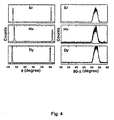
- Fig. 4 shows representative x-ray diffraction ⁇ -scans of the (103) peak for several (RE)BCO films, including Er-, Ho-, and Dy-BCO (left panels).
- the right panel plots display the ⁇ -scans for (RE)BCO films taken about the (104) peak.
- Fig. 5 shows a higher sensitivity ⁇ -scan of the (103) Bragg angle for a Dy-BCO thin film.
- Fig. 6 shows an atomic force microscope (AFM) scan of the surface of a Dy-BCO thin film that is optimized for RF properties.
- AFM atomic force microscope
- Fig. 7 shows an AFM scan of the surface of a Ho-BCO thin film that is optimized for RF properties.
- Fig. 8 shows an AFM scan of the surface of a Er-BCO thin film that is optimized for RF properties.
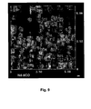
- Fig. 9 shows an AFM scan of the surface of a Nd-BCO thin film that is optimized for RF properties.
- Fig. 10 displays the room-temperature (300 K) dc resistivity values as a function of the Ba/RE ratio for different compositions of the various (RE)BCO thin films indicated.
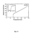
- Fig. 11 shows the dc resistivity as a function of temperature, ⁇ ( T ), for a Dy-BCO film optimized for RF properties. A detail of the superconducting transition is shown in the inset.
- Fig. 12 shows the ⁇ ( T ) curve for a Ho-BCO film optimized for RF properties. A detail of the superconducting transition is shown in the inset.
- Fig. 13 shows the ⁇ ( T ) curve for a Er-BCO film optimized for RF properties. A detail of the superconducting transition is shown in the inset.
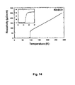
- Fig. 14 shows the ⁇ ( T ) curve for a Nd-BCO film optimized for RF properties. A detail of the superconducting transition is shown in the inset.
- Fig. 15 displays the zero-resistance T c values as a function of the Ba/RE ratio for different compositions of the various (RE)BCO thin films indicated.
- Fig. 16 shows the geometry of the quasi-lumped element resonator design used to measure the Q values of our (RE)BCO films.
- This resonator has a center frequency of about 1.85 GHz for films on MgO substrates.
- the resonator dimensions are 5.08-mm square.
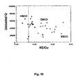
- Fig.17 displays the unloaded quality factor ( Q u ) as a function of the Ba/RE ratio for different compositions of the various (RE)BCO thin films indicated. These Q u values were measured at a temperature of 67 K and input power of -10 dBm for lumped-element RF resonators having a center frequency of about 1.85 GHz.
- the dotted line at Ba/RE 2 represents the on-stoichiometric value of the 1:2:3 compound.
- Fig. 19 displays the Q u values as a function of the Ba/Cu ratio for different compositions of the various (RE)BCO thin films indicated. These Q u values were measured at a temperature of 67 K and input power of -10 dBm for lumped-element RF resonators having a center frequency of about 1.85 GHz.
- Fig. 20 shows the layout of the 10-pole B-band cellular filter design used for our IMD tests.
- the filter dimensions are 18-mm by 34-mm.
- Fig. 21 shows a block diagram for an intermodulation distortion measurement of an HTS filter.
- Fig. 22 shows the typical S 11 response of a 10-pole B-band cellular RF filter fabricated from a (RE)BCO thin film. The positions of the input frequencies for three two-tone intermodulation distortion test measurements are shown.
- Fig. 23 shows the results of intermodulation distortion (IMD) test measurements made at 79.5 K as a function of the Ba/Dy ratio for several 10-pole B-band filters patterned from Dy-BCO films.
- IMD intermodulation distortion
- Fig. 24 shows the results of IMD test measurements made at 79.5 K as a function of the Ba/Ho ratio for several 10-pole B-band filters patterned from Ho-BCO films.
- the dotted lines indicate the required specification levels.
- Fig. 25 shows the results of IMD test measurements made at 79.5 K as a function of the Ba/Er ratio for several 10-pole B-band filters patterned from Er-BCO films.
- the dotted lines indicate the required specification levels.
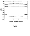
- Fig. 26 shows the results of IMD test measurements made at 79.5 K for four 10-pole B-band filters patterned from Nd-BCO films. The dotted lines indicate the required specification levels.
- Fig. 27 displays the unloaded quality factor ( Q u ) as a function of the Ba/Dy ratio for different compositions of the various Dy-BCO thin films indicated. These Q u values were measured at a temperature of 67 K and input power of -10 dBm for lumped-element RF resonators having a center frequency of about 1.85 GHz.
- the solid line at Ba/Dy 2 represents the on-stoichiometric value of the 1:2:3 compound.
- Fig. 28 displays the unloaded quality factor ( Q u ) as a function of the Ba/Dy ratio for different compositions of the various Dy-BCO thin films indicated. These Q u values were measured at a temperature of 77 K and input power of -10 dBm for lumped-element RF resonators having a center frequency of about 1.85 GHz.
- the solid line at Ba/Dy 2 represents the on-stoichiometric value of the 1:2:3 compound.
- Fig. 29 displays the ratio of high input power (+10 dBm) to low input power (-10 dBm) Q factors for different compositions of the various Dy-BCO thin films indicated wherein the Q u values were measured at a temperature of 67 K.
- Fig. 30 displays the ratio of high power to low power Q factors for different compositions of the various Dy-BCO thin films indicated wherein the Q u values were measured at a temperature of 77 K.
- Fig. 31 displays the 2 ⁇ (005) x-ray peak intensities as a function of the Ba/Dy ratio for different compositions of Dy-BCO thin films.
- Fig. 32 displays the room-temperature (300 K) dc resistivity values as a function of the Ba/Dy ratio for different compositions of Dy-BCO thin films.
- Fig. 33 displays the zero-resistance T c values as a function of the Ba/Dy ratio for different compositions of Dy-BCO thin films.
- Table I displays the maximum Q u values at ⁇ 1.85 GHz obtained for several of our (RE)BCO thin films measured using a patterned test resonator. The measurements were made at 67 K and 77 K for an input power of -10 dBm. This table also shows the R s values that we have calculated from these Q u values. Table I. Unloaded Q values of our highest- Q films measured with our standard test resonator at -10 dBm input power. The R s values are calculated from these measured Q values. These calculated R s values of the patterned structures are less than the actual measured R s values of the bulk films.
- this invention relates to high temperature superconducting (HTS) thin films with compositions that are optimized for RF/microwave applications and methods for reliably producing such films.
- the invention is characterized in terms of its physical composition, surface morphology, superconducting properties, and performance characteristics of microwave circuits made from these films (filters, delay lines, couplers, etc.; particularly bandpass and bandreject filters, more particularly bandpass and bandreject preselector filters for cellular telephone base station receivers).
- the distinction between HTS (RE)BCO films of the prior art and the (RE)BCO films of this invention is found both in the composition that deviates significantly from the 1:2:3 stoichiometry and the highly optimized RF properties of the new composition.
- a thin film may be defined as a layer (generally, very thin) of a material that is grown, deposited, or otherwise applied to a suitable supporting substrate.
- the thickness of this film may range from about one nm (10 -9 m) to several ⁇ m (>10 -6 m) thick.
- the typical range of thin film thickness for many applications is from 100 nm to 1000 nm.
- High temperature superconductors encompass a broad class of ceramic materials, typically oxides, more typically copper oxides or cuprates, that have a transition temperature or critical temperature, T c , below which these materials are superconducting. Above this critical temperature, they generally behave as metallic, or "normal,” conducting materials. HTS materials are further generally characterized as having T c values above about 30 K. Examples of HTS materials include La 2 CaCu 2 O 6 , Bi 2 Sr 2 CaCu 2 O 8 , YBa 2 Cu 3 O 7 , Tl 2 Ba 2 CaCu 2 O 8 , HgBa 2 CaCu 2 O 7 , etc. These materials must have a well-defined crystal structure in order to be superconducting, i.e., they must have a very specific regular and repeated arrangement of their constituent atoms.
- the rare earth (RE) elements are the 15 lanthanide elements with atomic numbers 57 through 71 that are in Group IIIA of the Periodic Table: lanthanum, cerium, praseodymium, neodymium, promethium, samarium, europium, gadolinium, terbium, dysprosium, holmium, erbium, thulium, ytterbium, and lutetium.
- Yttrium (atomic number 39) a Group IIIA transition metal, although not a lanthanide is generally included with the REs as it occurs with them in natural minerals and has similar chemical properties. Commonly included with the REs because of their similar properties are scandium (atomic number 21), also a Group IIIA transition metal, and thorium (atomic number 90), an element in the actinide series of the Periodic Table.
- the most ubiquitous HTS material is YBCO, which consists of an ordered amount and arrangement of Y, Ba, Cu, and O atoms.
- the fundamental repeated unit of this material's specific atomic arrangement is known as the unit cell, consisting nominally of one Y, two Ba, three Cu, and seven O atoms.
- the atomic ratios needed to form this compound are described by the chemical formula YBa 2 Cu 3 O 7- ⁇ , where the oxygen content is variable between 6 and 7 atoms per unit cell, or 0 ⁇ ⁇ ⁇ 1.
- the T c value is determined largely by the value of ⁇ .
- YBCO is a superconductor for ⁇ ⁇ ⁇ 0.6, with values of ⁇ near 0 being generally preferred in order to provide the highest T c values.
- YBCO is the most widely studied HTS material, and much is known about how to make it in single phase form, i.e., consisting of solely the composition mentioned above and containing no other phases.
- many other similar compounds can also be fabricated that may have similar or superior superconducting properties, depending on the application.
- These compounds may have Y:Ba:Cu ratios that are different from 1:2:3, and they may also consist of elements other than Y or Ba.
- a generalized nomenclature for the makeup of this compound may thus be written as M' x M y Cu 3 O 7- ⁇ , where M' may in general be any essentially trivalent ion or combination of ions, and M may be any essentially divalent ion or combination of ions.
- the ratios of M':Cu, M:Cu, and M':M may also vary substantially from the nominal values of 1:3, 2:3, and 1:2, respectively. While the full range of parameter space has not been explored, it is reasonable to believe that compounds with cation ratios deviating from the nominal by as much as 50% may still be superconductors, e.g. 1:6 ⁇ M':Cu ⁇ 1:2, 1:3 ⁇ M:Cu ⁇ 1:1, and 1:4 ⁇ M':M ⁇ 3:4. However, significantly altering the composition from the 1:2:3 stoichiometry does affect the specific properties of the composition including critical current density ( J c ), normal-state resistivity ( ⁇ ), critical temperature ( T c ), and surface resistance ( R s ).
- J c critical current density
- ⁇ normal-state resistivity
- T c critical temperature
- R s surface resistance
- Ba is generally preferred as the divalent element, or M in the above formula. Full or partial substitutions of many elements for Ba tend to decrease T c or destroy superconductivity altogether. These elements include Sr, La, Pr and Eu. ( Y. Xu, Physica C 341-348, pp 613-4 (2000 ) and X.S. Wu, Physica C 315, pp 215-222 (1999 ).
- the Cu atoms may be doped with Co, Zn, Ni, etc., the effect of most of which is to decrease T c , though the absolute effect (e.g., charge transfer or disruption of superconductivity on the Cu-O planes) depends on whether the Cu(I) or Cu(2) sites are affected.
- the absolute effect e.g., charge transfer or disruption of superconductivity on the Cu-O planes
- Some partial substitutions on the Y sites may have a similar effect, such as Ca, Ce, and Pr ( L. Tung, Phys. Rev. B Vol 59, No. 6, pp 4504-4512 (1999 ) and C.R. Fincher, Phys. Rev. Lett.
- compositions may be altered substantially from the nominal 1:2:3 stoichiometry in order to tailor their properties for specific applications. For example, compositions near 1:2:3 may be preferred for multilayer or active device applications for which smooth thin film surfaces are of paramount importance.
- optimization of HTS films for RF applications requires the production of thin films that strike a balance between having the lowest possible RF surface resistance ( R s ) values and the lowest RF nonlinearities that are achievable. This in turn often requires the fabrication of (RE)BCO films that deviate significantly from the 1:2:3 composition.
- the HTS thin films of this invention are optimized for RF applications, and as such they have the lowest possible RF surface resistance ( R s ) values and the lowest possible RF nonlinearities.
- the film compositions have the nominal formula (RE) x Ba y Cu 3 O 7- ⁇ , where RE is one of the previously defined rare earth elements, preferably Dy, and where the ratio y : x is between about 1.5 - 1.8, preferably between about 1.55 - 1.75, and more preferably between about 1.6 - 1.7.
- HTS materials are extremely sensitive to their degree of crystalline perfection. This places severe constraints on the choice of a suitable substrate material on which high-quality HTS films may be grown. Some of these constraints include crystal structure, compatibility with the growth process, chemical compatibility, compatibility with the application, as well as other requirements imposed by nature.
- the substrate must have an appropriate lattice match with the HTS film such that epitaxial growth of the film can occur and a well-oriented film will form. A poor lattice match can lead to dislocations, defects, and misoriented grains in the film. In general, the substrate should be available in single-crystal form in order to meet these requirements.
- the substrate must be able to withstand the high processing temperatures during the growth process that are required for the crystallization of the HTS compound.
- structural integrity and a reasonable thermal expansion match with the HTS film is required in order to prevent strain and cracking of the film during the cool down cycle from the growth temperature or from any other subsequent thermal cyclings.
- the substrate must be chemically compatible with (RE)BCO, non-reactive, and with minimal diffusion into the film at high temperature.
- the substrate must be available in a size large enough for the intended use of the HTS thin film. For example, certain passive microwave circuits or high-volume electronics applications require a large substrate size. A minimum substrate of 5.08 cm (2") in diameter is typical for these applications, though larger sizes are often desirable if available.
- the substrate may also be required to have physical properties that are compatible with experimental measurement techniques or applications. For most applications the substrates should be stable, mechanically robust insulators. Other requirements may include transparency in the infrared for optical transmission measurements, constituent elements or structure that do not interfere with spectroscopic measurements such as Rutherford backscattering (RBS) or energy-dispersive x-ray analysis (EDX), and a low dielectric constant and loss tangent for microwave measurements and applications at the intended temperature of operation.
- RBS Rutherford backscattering
- EDX energy-dispersive x-ray analysis
- Al 2 O 3 is a low-loss substrate and is widely available in several different orientations and sizes. However, it reacts strongly with (RE)BCO at high temperatures, requiring the use of an appropriate buffer layer. In addition, Al 2 O 3 has a poor thermal expansion match to (RE)BCO, causing a tendency for the films to crack upon cooldown. MgO has relatively low loss and a good thermal expansion match to (RE)BCO, making it a good choice for RF applications. However, MgO has a much larger lattice mismatch than the other examples listed above, so that great care must be taken to insure that the (RE)BCO films grown on MgO are well oriented.
- (RE)BCO films grown on MgO it is relatively common for (RE)BCO films grown on MgO to contain in-plane-rotated grains and 45° grain boundaries.
- the minimization of the amount of these high-angle grain boundaries is mandatory for good microwave performance, particularly for high RF linearity.
- Certain MgO substrate surface treatments may be instituted to help control the number of high-angle grain boundaries, but greater effort is required to further suppress formation of these grain boundaries, particularly for demanding RF applications.
- the growth method, growth conditions, and particularly the composition of the (RE)BCO films must all be chosen and adjusted to minimize the amount of 45° grains in films grown on MgO.
- the anisotropic transport properties of (RE)BCO, its orthorhombic crystal structure, and its small superconductive coherence length mean that the (RE)BCO films must have excellent crystalline structure and orientation. This is particularly true in order to obtain good microwave properties. Hence, the films must be substantially free of secondary phases, they must possess good epitaxy both in-plane (parallel to the substrate surface) and out-of-plane (perpendicular to the substrate surface). Typically, the c-axis of (RE)BCO is aligned perpendicular to the substrate surface. All the grains in the film must be so aligned, and they must be highly aligned with respect to one another.
- the degree of this crystalline order is typically characterized by ⁇ - 2 ⁇ x-ray diffraction scans, where the requirements are the existence of only c-axis-oriented (00 l ) spectral lines having narrow peak widths, and also narrow peak widths of the so-called ⁇ -scan, or rocking curve scan about a given Bragg angle.
- the ⁇ -2 ⁇ measurement can also detect the presence of spectral lines due to a -axis-oriented grains within the film. These grains may also be detected by a ⁇ -scan about an appropriate Bragg angle.
- the amount of a -axis grains in the film is ideally zero, so that the intensity of a -axis x-ray peaks relative to c-axis x-ray peaks for a c -axis-oriented film is ideally zero, and preferably much less than 1%.
- the c -axis-oriented grains should also be in-plane oriented, meaning that they are in registry with each other and with the substrate crystal structure. Grains that are rotated with respect to the overall in-plane lattice structure lead to nonzero-degree angle grain boundaries.
- Fig. 1 shows the ⁇ -2 ⁇ scans for several 700-nm-thick (RE)BCO films made by us and optimized for RF applications.
- these films include RE substitutions of Er (EBCO), Ho (HBCO), Dy (DBCO), and Nd (NBCO).
- the x-ray scans display the presence of only (00 l ) peaks, indicating that the films are single-phase and highly c-axis aligned, and that no a-axis-oriented grains exist in the films. Note that the relative peak intensities of the (RE)BCO films are different from YBCO, indicative of the effect of the different RE ionic radii.
- Fig. 2 shows the (005) peak positions vs.
- Fig. 3 shows the intensities of the (005) peaks for these films.
- Fig. 31 shows the intensities of the (005) peaks for DBCO films of varying compositions as a function of the Ba/Dy ratio.
- These DBCO films are inclusive of those shown in Fig. 3 , but are not necessarily optimized for RF properties.
- high peak intensities, indicative of good crystallinity are obtained for DBCO film compositions that deviate significantly from the on-stochiometric ratio indicated by the solid line on the graph.
- FIG. 4 shows representative ⁇ -scans of the (103) peak for several (RE)BCO films (left hand panels). Note that any peaks at 45° are absent, indicating an absence of 45° oriented grains and grain boundaries.
- Fig. 5 shows a higher sensitivity ⁇ -scan for one of our Dy-BCO films. The y-axis is plotted on a log scale, and it can be seen that only very weak peaks occur at 45° relative to the main peak. This scan indicates the degree to which this film is free from high-angle grain boundaries. The intensity of the weak lines at 45° is only about 0.012% of the maximum central peak indicating that almost none of the grains are misaligned. This is important for optimization of the RF properties of these films, most notably their RF nonlinearities.
- the right-hand panel of Fig. 4 displays the ⁇ -scans for (RE)BCO films taken about the (104) peak; as indicated in Fig. 1 , these scans also demonstrate the absence of a -axis-oriented grains
- the surface morphology of (RE)BCO thin films is typically measured by scanning probe profilometry, atomic force microscopy (AFM), and scanning electron microscopy (SEM).
- AFM atomic force microscopy
- SEM scanning electron microscopy
- smooth films are preferred for applications, though some degree of surface roughness may be tolerated in deference to the optimization of other important properties such as J c and R s .
- Figs. 6-9 show typical AFM images of Dy-, Ho-, Er-, and Nd-BCO films over a 5 ⁇ m ⁇ 5 ⁇ m area. These films have been optimized in terms of their RF properties. The RMS surface roughness for these films is a few nm.
- Fig. 6 shows the surface morphology for a high- Q DBCO film with very low RF nonlinearities. The grain size of this film can be seen to be roughly 2 ⁇ m in diameter.
- the optimized EBCO surface depicted in Fig. 8 has a smaller grain size still, and in this case there also exist CuO particulates.
- the grains of the NBCO film of Fig. 9 are also square in appearance and have a size of less than 0.5 ⁇ m.
- the different surface morphologies for these optimized (RE)BCO films are in general reflections of the different composition and growth conditions needed to achieve the best RF properties for the different RE substitutions.
- the (RE)BCO films are further characterized by measuring their composition and their electrical properties, including the dc resistivity ( ⁇ ) as a function of temperature [ ⁇ ( T )], T c value and transition width, critical current density ( J c ), and RF surface resistance ( R s ).
- the films are also subsequently patterned into RF circuits for which we measure the unloaded quality factor (Q) values, intermodulation distortion (IMD), and nonlinear critical current density ( J IMD ) ⁇
- the composition of the films of this invention was measured using Rutherford backscattering spectrometry (RBS) and inductively coupled plasma spectroscopy (ICP). These techniques are both capable of a high degree of accuracy and precision, though achieving a measurement accuracy of 1 ⁇ or 2 ⁇ equal to 1% is a difficult task and requires more care than is the norm for these techniques.
- RBS Rutherford backscattering spectrometry
- ICP inductively coupled plasma spectroscopy
- the ion energies are typically in the range of several hundred to several thousand keV, and the energy of a backscattered ion depends on the mass of the target atom with which it has collided.
- the energy spectrum of the backscattered ions allows identification of the elements comprising the sample and their ratios (stoichiometry).
- the incident ions traverse the sample, they lose energy due to inelastic scattering with electrons. This energy loss occurs in a known way and therefore allows determination of sample composition as a function of depth.
- the spectral peaks of the measured constituent elements can overlap, requiring careful fitting of the spectra to extract the composition, and this procedure involves uncertainty and can introduce error.
- the thin films are digested in an acidic solution which is then introduced into a high-temperature (up to 10,000 °C) plasma discharge.
- the plasma ionizes and excites the constituent atoms in the solution, and as these atoms decay to a lower energy state, they emit light of a characteristic wavelength that can be detected by a high-resolution spectrometer.
- ICP-AES atomic emission or optical emission spectroscopy
- the dc resistivity p is measured by a standard four-point-probe technique.
- the room-temperature resistivity of high-quality (RE)BCO films is typically between 150 and 300 ⁇ cm, though this value varies as a function of RE element and of film composition.
- Fig. 10 shows the room-temperature (300 K) resistivity values of several (RE)BCO films as a function of composition, specifically the Ba/RE ratio.
- Fig. 32 shows the room-temperature resistivity values for several DBCO films as a function of the Ba/Dy ratio.
- These DBCO films are inclusive of those shown in Fig. 10 , but are not necessarily optimized for RF properties
- the room temperature resistivity values indicative of high quality films are obtained for DBCO film compositions that deviate significantly from the on-stochiometric ratio (indicated by the solid line on the graph), particularly within Ba/Dy ratios ranging between about 1.5-1.8, with particularly good resistivity values achieved for a Ba/Dy ratio of 1.76.
- the temperature dependence of the resistivity is shown in Figs. 11-14 for several (RE)BCO films.
- the temperature dependence of p for good films is typically linear or slightly downwardly bowed indicative of so-called overdoped behavior, as these plots indicate.
- the measurement of ⁇ ( T ) is also used to determine both the width (in temperature) of the transition to the superconducting state and the zero-resistance T c value.
- the detail of the superconducting transition region of these films is shown in the inset of Figs. 11-14 .
- the T c values for (RE)BCO films are typically between 87 and 91 K ( Figs.
- the T c values of the (RE)BCO samples prepared by the process of this invention are 88.5(5), 88.9(5), 89.2(5), 89.6(5), and 94.5(8) K for Er, Y, Ho, Dy, and Nd, respectively. These values were measured immediately following deposition. Since the films are oxygen overdoped as judged by the slope of the R-T curves, the measured T c values are slightly lower than the highest values known for these compounds.
- Fig. 15 plots the T c values for different compositions of our Ho-, Er-, and Dy-BCO films.
- Fig. 33 plots the T c values for different compositions of additional DBCO films. These DBCO films are inclusive of those shown in Fig. 15 , but are not necessarily optimized for RF properties. It can be seen that high T c values are obtained even for compositions deviating substantially from the on-stoichiometric (1:2:3) value, indicated by the solid vertical line.
- the RF surface resistance of (RE)BCO thin films may be measured in a number of ways, including cavity or parallel plate resonator techniques using bulk (unpatterned) films.
- R s is typically measured at frequencies between a few hundred MHz and 10s of GHz.
- R s may also be extracted from the Q measurements of patterned resonators of various kinds, e.g., microstrip, quasi-lumped element, etc. Extraction of R s from the measured Q values of these structures requires careful modeling of the resonator performance to determine the geometric parameter ⁇ Q .
- R s ⁇ 0 ⁇ ⁇ Q ⁇ 1 Q
- w0 the resonant frequency
- ⁇ Q is a parameter that depends only on the resonator geometry
- Q is the measured unloaded quality factor of the resonator.
- the extracted R s value of patterned structures is typically higher than the R s value obtained by direct measurement of the bulk films in an RF cavity. This may be caused by patterning the film, which may introduce defects that can add additional resistive RF losses in the Q measurement. It may also arise from uncertainties in ⁇ Q or the non-uniformity of the current density in microstrip resonators which is generally not present in bulk film measurement systems.
- the Q u was measured for a range of composition and growth conditions of each (RE)BCO material, and the growth conditions and composition of each material were optimized to achieve maximum Q u .
- Q u values that are sufficient for cellular microwave applications for Dy-BCO, Er-BCO, Ho-BCO and Nd-BCO thin films. Indeed, for 700-nm-thick films, we have achieved unloaded Q values over 40,000 at 1.85 GHz, 67 K, and -10 dBm input power for our test resonator structure using each of these materials.
- Our Nd-BCO films display higher Q u values at 67 K, reaching 80,000 (not shown on this plot), comparable to the highest Qs obtained with YBCO films. At 77 K, the Q values of Nd-BCO films can exceed those of YBCO.
- Table I displays the maximum Q u values obtained for test resonators made from our (RE)BCO films measured at 67 K and 77 K for an input power of -10 dBm. This table also shows the R s values that we have calculated from these Q u values.
- Fig. 27 displays additional data on the unloaded quality factor ( Q u ) as a function of the Ba/Dy ratio for different compositions of the various DBCO thin films indicated.
- These DBCO films are inclusive of those shown in Fig. 17 , but are not necessarily optimized for RF properties.
- Fig. 17 represents the best Q values obtainable at each composition
- Fig. 27 shows a range of Q values at each composition, because other properties of the films may not be optimized, e.g., growth temperature, film thickness, surface morphology, or crystallinity.
- These Q u values were measured at a temperature of 67 K and input power of -10 dBm for lumped-element RF resonators having a center frequency of about 1.85 GHz.
- Fig. 28 displays the unloaded quality factor ( Q u ) as a function of the Ba/Dy ratio for the same DBCO thin films of varying compositions measured at a temperature of 77 K and input power of -10 dBm.
- Fig. 30 plots the ratio of Q measured at high power to low power at 77 K for several DBCO films of varying composition. This figure also shows that excellent power handling is obtained even for compositions that deviate substantially from the on-stoichiometric value.
- the input power levels to the (RE)BCO filter also affects their performance by generating different amounts of intermodulation distortion, as described belows.
- FIG. 20 shows a layout of the filter design. The filters were tuned, and their performance was evaluated in terms of insertion loss, return loss, and out-of-band rejection. In addition, we used these 10-pole filters to measure the nonlinear properties of these materials in terms of their third-order intermodulation distortion (IMD).
- IMD intermodulation distortion
- the location of these input tones is in-band, far from the band edge, or close to the band edge.
- the output power of the third-order mixing product at frequency 2 f 1 - f 2 is then measured in a spectrum analyzer.
- the magnitude of the output signal from the filter at these frequencies is an important measure of the RF nonlinearities of the filter and determines its suitability for many microwave applications.
- the presence of intermodulation distortion reflects the current density dependence of the surface reactance, X s , of the superconducting thin film ( T. Dahm & D.J. Scalapino, J. Appl. Phys. 81 (4), pp 2002-2009) (1997 ).
- Fig. 23 shows the IMD values measured at 79.5 K as a function of Ba/Dy ratio for several 10-pole B-band filters patterned from optimized Dy-BCO films. Note that all the filters measured meet the requirements, which are indicated by dotted lines.
- Figs. 24 and 25 show the IMD values as a function of the Ba/RE ratio measured at 79.5 K for several 10-pole B-band filters patterned from optimized Ho-BCO and Er-BCO films.
- Fig. 26 shows the IMD values measured at 79.5 K for four 10-pole B-band filters patterned from optimized Nd-BCO films. Intermodulation distortion in HTS filters arises due to nonlinearity of the microwave surface reactance, X s , of the thin films.
- the out-of -band IMD test requirement corresponds to a minimum J IMD in the HTS thin film of 1 ⁇ 10 7 A/cm 2 .
- the DBCO films surpass the specification by 14 dB, which here corresponds to a factor of 5.
- the DBCO films have a J IMD of 5 ⁇ 10 7 A/cm 2 .
- J IMD in HTS thin films must be > 1 ⁇ 10 7 A/cm 2 , more preferably > 2 ⁇ 10 7 A/cm 2 , and most preferably > 3 ⁇ 10 7 A/cm 2 .
- Our substrates are typically MgO single crystals up to 5.08 cm (2") in diameter that are rotated continuously between the window and the oxidation pocket at 300 rpm.
- the chamber ambient pressure away from the pocket is ⁇ 1.33 mPa ( ⁇ 10 -5 ) Torr.
- This configuration provides sufficient oxygen pressure for stability of the high- T c phase while the metallic evaporation sources are simultaneously free from oxidation, and the evaporated species are free from scattering.
- the rare earth elements Er, Ho, and Dy are evaporated from electron beam sources, Nd and Cu are evaporated from either electron beam sources or resistive sources, and Ba is evaporated from a thermal furnace or a resistive source.
- the typical deposition rate is 0.25 mm/s ( ⁇ 2.5 ⁇ /sec.)
- the deposition temperature for the films discussed here is 760 to 790°C, and the film thickness is about 700 nm.
- the films were deposited directly onto MgO substrates, with the exception ofNd-BCO, which presently requires a thin buffer layer in order to achieve the best results.
- the oxygen pocket pressure and deposition rate used to achieve optimal results are similar for the (RE)BCO films that we have studied.
- the best substrate temperatures for Er, Ho, Dy, and Nd are 780, 790, 790, and 780 °C, respectively. These temperatures are significantly higher than the temperature of 760 °C we use to achieve optimal RF properties for YBCO.
- the use of different growth conditions for the (RE)BCO materials compared to YBCO is mandatory in order to achieve the very best RF properties. For example, higher growth temperatures for the (RE)BCO materials as compared to YBCO are generally required in order to insure the absence of deleterious misaligned grains.
- the composition must also be optimized for this purpose, as we have discussed.
- RF properties including a) growth temperature, b) growth rate, c) oxygen pressure, and d) stoichiometry.
- Specific choices for (a), (b), and (c) may yield different optimized properties and different optimized compositions.
Landscapes
- Engineering & Computer Science (AREA)
- Chemical & Material Sciences (AREA)
- Manufacturing & Machinery (AREA)
- Ceramic Engineering (AREA)
- Electromagnetism (AREA)
- Physics & Mathematics (AREA)
- Organic Chemistry (AREA)
- Structural Engineering (AREA)
- Materials Engineering (AREA)
- Power Engineering (AREA)
- Crystallography & Structural Chemistry (AREA)
- Superconductors And Manufacturing Methods Therefor (AREA)
- Inorganic Compounds Of Heavy Metals (AREA)
- Superconductor Devices And Manufacturing Methods Thereof (AREA)
- Physical Vapour Deposition (AREA)
Claims (16)
- Supraleitender Gegenstand, der aufweist:ein Substrat; undeine auf dem Substrat abgeschiedene dünne Schicht mit der nominalen Zusammensetzung REzBayCu3Ox;worin RE ein Seltenerdmetall bedeutet;worin x zwischen 6 und 7 liegt, wobei die Grenzen eingeschlossen sind;worin y kleiner als in etwa 2,1 ist und das Verhältnis y/z 1,65 ± 10 % beträgt;undworin die dünne Schicht eine Supraleitungsübergangstemperatur > 87 K aufweist.
- Supraleitender Gegenstand nach Anspruch 1, worin JIMD > 0,8 x 10⁷ A/cm2 bei 77 K ist.
- Supraleitender Gegenstand nach Anspruch 2, worin JIMD > 1,5 x 10⁷ A/cm2 bei 77 K ist.
- Supraleitender Gegenstand nach Anspruch 3, worin JIMD > 3 x 10⁷ A/cm2 bei 77 K ist.
- Supraleitender Gegenstand nach einem der vorhergehenden Ansprüche, worin der bei 1,85 GHz und 77 K gemessene Wert RS < 15 µΩ ist.
- Supraleitender Gegenstand nach Anspruch 5, worin der bei 1,85 GHz und 77 K gemessene Wert RS < 10 µΩ ist.
- Supraleitender Gegenstand nach Anspruch 6, worin der bei 1,85 GHz und 77 K gemessene Wert RS < 8 µΩ ist.
- Supraleitender Gegenstand nach einem der vorhergehenden Ansprüche, worin RE Dy bedeutet.
- Supraleitender Gegenstand nach Anspruch 1, worin RE Nd ist.
- Supraleitender Gegenstand nach einem der vorhergehenden Ansprüche, worin das Verhältnis y/z 1,65 ± 6 % ist.
- Supraleitender Gegenstand nach Anspruch 10, worin das Verhältnis y/z 1,65 ± 3 % ist.
- Supraleitender Gegenstand nach einem der Ansprüche 1, 8 oder 11, worin JIMD bei 850 MHz > 0,8 x 10⁷ A/cm2 bei 77 K ist.
- Supraleitender Gegenstand nach einem der vorhergehenden Ansprüche, wobei der Gegenstand 45-Grad-Korngrenzen in einer Konzentration < 0,02% aufweist.
- Supraleitender Gegenstand nach einem der vorhergehenden Ansprüche, wobei die dünne Schicht auf dem Substrat durch reaktive Koevaporation abgeschieden ist.
- Supraleitender Gegenstand nach einem der vorhergehenden Ansprüche, wobei das Substrat eine Oberfläche von mehr als 19,4 cm2 (3 Quadratzoll) aufweist.
- Supraleitender Gegenstand nach einem der vorhergehenden Ansprüche, wobei die dünne Schicht in Form eines Hochfrequenzschaltkreises mit Schaltelementen mit hohem Q-Faktor strukturiert ist.
Applications Claiming Priority (2)
| Application Number | Priority Date | Filing Date | Title |
|---|---|---|---|
| US63904304P | 2004-12-23 | 2004-12-23 | |
| PCT/US2005/047147 WO2006071899A2 (en) | 2004-12-23 | 2005-12-22 | Rf-properties-optimized compositions of (re)ba2cu3o7-d thin film superconductors |
Publications (3)
| Publication Number | Publication Date |
|---|---|
| EP1843988A2 EP1843988A2 (de) | 2007-10-17 |
| EP1843988A4 EP1843988A4 (de) | 2011-11-02 |
| EP1843988B1 true EP1843988B1 (de) | 2013-02-13 |
Family
ID=36615496
Family Applications (1)
| Application Number | Title | Priority Date | Filing Date |
|---|---|---|---|
| EP05855665A Ceased EP1843988B1 (de) | 2004-12-23 | 2005-12-22 | Hinsichtlich hf-eigenschaften optimierte zusammensetzungen von (re)ba2cu3o7-d-dünnfilm-supraleitern |
Country Status (6)
| Country | Link |
|---|---|
| US (4) | US7867950B2 (de) |
| EP (1) | EP1843988B1 (de) |
| JP (1) | JP5243800B2 (de) |
| KR (1) | KR101372059B1 (de) |
| CN (2) | CN101728019B (de) |
| WO (1) | WO2006071899A2 (de) |
Families Citing this family (12)
| Publication number | Priority date | Publication date | Assignee | Title |
|---|---|---|---|---|
| US7867950B2 (en) * | 2004-12-23 | 2011-01-11 | Superconductor Technologies, Inc. | RF-properties-optimized compositions of (RE)Ba2Cu3O7-δ thin film superconductors |
| JP5270176B2 (ja) * | 2008-01-08 | 2013-08-21 | 公益財団法人国際超電導産業技術研究センター | Re系酸化物超電導線材及びその製造方法 |
| US8391937B1 (en) | 2008-03-05 | 2013-03-05 | The United States Of America As Represented By The Secretary Of The Navy | Radio frequency cavities lined with superconductor-coated tiles |
| US9012848B2 (en) * | 2012-10-02 | 2015-04-21 | Coherent, Inc. | Laser power and energy sensor utilizing anisotropic thermoelectric material |
| US9059346B2 (en) * | 2012-10-02 | 2015-06-16 | Coherent, Inc. | Laser power and energy sensor utilizing anisotropic thermoelectric material |
| CN105572106A (zh) * | 2015-12-18 | 2016-05-11 | 苏州新材料研究所有限公司 | 一种测定ReBCO高温超导薄膜组成的方法 |
| US20170279028A1 (en) * | 2016-03-22 | 2017-09-28 | Eastern Plus, LLC | Purposing and repurposing a group of compounds that can be used as high temperature superconductors |
| CN108588648A (zh) * | 2017-12-29 | 2018-09-28 | 上海大学 | 异位多元金属氧化物薄膜外延生长及其连续化制备的方法 |
| CN108677145A (zh) * | 2018-04-17 | 2018-10-19 | 上海大学 | 异位多元金属氧化物薄膜外延生长及其连续化制备的方法 |
| CN111983319B (zh) * | 2020-08-14 | 2023-03-14 | 电子科技大学 | 一种金属材料微波表面电阻率高温测试装置及测试方法 |
| WO2022236068A1 (en) * | 2021-05-07 | 2022-11-10 | Cornell University | Method for protecting reactive materials with atomically thin film |
| CN116143499B (zh) * | 2022-12-08 | 2024-08-09 | 广东工业大学 | 一种用于固化锝的锝酸钡陶瓷固化体及其制备方法和应用 |
Family Cites Families (30)
| Publication number | Priority date | Publication date | Assignee | Title |
|---|---|---|---|---|
| US6635603B1 (en) * | 1987-01-09 | 2003-10-21 | Lucent Technologies Inc. | Devices and systems based on novel superconducting material |
| US6630425B1 (en) * | 1987-01-09 | 2003-10-07 | Lucent Technologies Inc. | Devices and systems based on novel superconducting material |
| US6638894B1 (en) * | 1987-01-09 | 2003-10-28 | Lucent Technologies Inc. | Devices and systems based on novel superconducting material |
| AU1425588A (en) | 1987-01-12 | 1988-07-27 | University Of Houston-University Park | Superconductivity in square-planar compound systems |
| US7056866B1 (en) | 1987-01-12 | 2006-06-06 | University Of Houston-University Park | Superconductivity in square-planar compound systems |
| EP0275343A1 (de) | 1987-01-23 | 1988-07-27 | International Business Machines Corporation | Supraleitender Verbund des Strukturtypes von K2NiF4 mit hoher Übergangstemperatur und Verfahren zu seiner Herstellung |
| JP2711253B2 (ja) * | 1987-03-18 | 1998-02-10 | インターナショナル・ビジネス・マシーンズ・コーポレーション | 超伝導膜及びその形成方法 |
| EP0284189B1 (de) * | 1987-03-23 | 1994-05-04 | Semiconductor Energy Laboratory Co., Ltd. | Verfahren zur Herstellung von supraleitenden Keramiken |
| EP0283620A1 (de) * | 1987-03-25 | 1988-09-28 | Semiconductor Energy Laboratory Co., Ltd. | Supraleitende Keramiken |
| EP0287749A1 (de) | 1987-04-23 | 1988-10-26 | International Business Machines Corporation | Mehrschichtige superleitende Kupferoxid-Verbindungen |
| US5071830A (en) * | 1988-08-31 | 1991-12-10 | Superconductor Technologies, Inc. | Metalorganic deposition method for forming epitaxial thallium-based copper oxide superconducting films |
| US5508255A (en) * | 1994-07-05 | 1996-04-16 | Superconductor Technologies, Inc. | Epitaxial thallium high temperature superconducting films formed via a nucleation layer |
| JPH0867968A (ja) * | 1994-08-26 | 1996-03-12 | Sumitomo Electric Ind Ltd | 酸化物薄膜の作製方法 |
| JP3207058B2 (ja) | 1994-11-07 | 2001-09-10 | 財団法人国際超電導産業技術研究センター | 超電導体薄膜及びその製造方法 |
| WO1998024944A1 (de) * | 1996-12-06 | 1998-06-11 | THEVA DüNNSCHICHTTECHNIK GMBH | Schichtmaterial sowie vorrichtung und verfahren zum herstellen von schichtmaterial |
| US6172007B1 (en) * | 1996-06-21 | 2001-01-09 | Dowa Mining Co., Ltd. | Oxide superconductor |
| JP2967154B2 (ja) * | 1996-08-02 | 1999-10-25 | 同和鉱業株式会社 | Agを含み結晶方位の揃った酸化物超電導体及びその製造方法 |
| US6022832A (en) * | 1997-09-23 | 2000-02-08 | American Superconductor Corporation | Low vacuum vapor process for producing superconductor articles with epitaxial layers |
| JP3767841B2 (ja) * | 1998-07-01 | 2006-04-19 | 財団法人国際超電導産業技術研究センター | 臨界電流密度の高い酸化物超電導体 |
| US6110278A (en) * | 1998-08-10 | 2000-08-29 | Saxena; Arjun N. | Methods for and products of growth of single-crystal on arrayed nucleation sites (SCANS) defined in nucleation unfriendly substrates |
| EP1006594A1 (de) * | 1998-12-03 | 2000-06-07 | Jochen Dieter Prof. Dr. Mannhart | Supraleiter mit verbesserter Stromdichte und Verfahren zu dessen Herstellung |
| DE19908597A1 (de) * | 1999-02-27 | 2000-09-14 | Aventis Res & Tech Gmbh & Co | Verfahren zum Vergüten eines Supraleitermaterials mit hoher Remanenzinduktion, vergütetes Supraleitermaterial und dessen Verwendung |
| EP1198849A2 (de) * | 1999-07-23 | 2002-04-24 | American Superconductor Corporation | Oberflächenbehandlungsprozess zur herstellung von vielschichtbauteilen |
| US6216941B1 (en) * | 2000-01-06 | 2001-04-17 | Trw Inc. | Method for forming high frequency connections to high temperature superconductor circuits and other fragile materials |
| US6527866B1 (en) * | 2000-02-09 | 2003-03-04 | Conductus, Inc. | Apparatus and method for deposition of thin films |
| US20020056401A1 (en) * | 2000-10-23 | 2002-05-16 | Rupich Martin W. | Precursor solutions and methods of using same |
| US20020119893A1 (en) * | 2001-02-27 | 2002-08-29 | Hughes Robert A. | Method of forming a superconductor |
| MXPA02001147A (es) * | 2001-03-19 | 2004-04-21 | Warner Lambert Co | Sintesis de ligandos bisfosina no-c2-simetricos como catalizadores para la hidrogenacion asimetrica. |
| CN2585868Y (zh) * | 2002-12-24 | 2003-11-12 | 中国科学院物理研究所 | 采用涡流加热靶材的共蒸发制备薄膜的装置 |
| US7867950B2 (en) * | 2004-12-23 | 2011-01-11 | Superconductor Technologies, Inc. | RF-properties-optimized compositions of (RE)Ba2Cu3O7-δ thin film superconductors |
-
2005
- 2005-12-22 US US11/317,889 patent/US7867950B2/en active Active
- 2005-12-22 CN CN2009102063593A patent/CN101728019B/zh not_active Expired - Fee Related
- 2005-12-22 CN CNB2005800473729A patent/CN100564312C/zh not_active Expired - Fee Related
- 2005-12-22 EP EP05855665A patent/EP1843988B1/de not_active Ceased
- 2005-12-22 JP JP2007548590A patent/JP5243800B2/ja not_active Expired - Fee Related
- 2005-12-22 KR KR1020077016832A patent/KR101372059B1/ko not_active Expired - Fee Related
- 2005-12-22 WO PCT/US2005/047147 patent/WO2006071899A2/en not_active Ceased
-
2010
- 2010-12-21 US US12/974,771 patent/US8716187B2/en active Active
-
2014
- 2014-04-17 US US14/255,129 patent/US20150051080A1/en not_active Abandoned
-
2015
- 2015-12-22 US US14/979,012 patent/US20160218269A1/en not_active Abandoned
Also Published As
| Publication number | Publication date |
|---|---|
| CN101111460A (zh) | 2008-01-23 |
| US20160218269A1 (en) | 2016-07-28 |
| US20110230356A1 (en) | 2011-09-22 |
| US20150051080A1 (en) | 2015-02-19 |
| CN100564312C (zh) | 2009-12-02 |
| JP5243800B2 (ja) | 2013-07-24 |
| US8716187B2 (en) | 2014-05-06 |
| US7867950B2 (en) | 2011-01-11 |
| CN101728019B (zh) | 2013-08-28 |
| CN101728019A (zh) | 2010-06-09 |
| WO2006071899A3 (en) | 2006-10-19 |
| US20060229211A1 (en) | 2006-10-12 |
| WO2006071899A2 (en) | 2006-07-06 |
| EP1843988A2 (de) | 2007-10-17 |
| JP2008546131A (ja) | 2008-12-18 |
| KR20070110268A (ko) | 2007-11-16 |
| KR101372059B1 (ko) | 2014-03-07 |
| HK1107806A1 (en) | 2008-04-18 |
| EP1843988A4 (de) | 2011-11-02 |
Similar Documents
| Publication | Publication Date | Title |
|---|---|---|
| US8716187B2 (en) | RF-properties-optimized compositions of (RE) Ba2Cu3O7-δthin film superconductors | |
| Adachi et al. | Superconducting (Sr, Nd) CuOy thin films with infinite-layer structure | |
| Sawa et al. | Electron-doped superconductor La 2− x Ce x CuO 4: Preparation of thin films and modified doping range for superconductivity | |
| US4996185A (en) | Ceramic superconducting thin film | |
| US6635603B1 (en) | Devices and systems based on novel superconducting material | |
| Lorenz et al. | Large-area and double-sided pulsed laser deposition of Y-Ba-Cu-O thin films applied to HTSC microwave devices | |
| US5130294A (en) | High temperature superconductor-calcium titanate structures | |
| Kim et al. | Properties of NdBa2Cu3O7− δ thin film prepared by off‐axis rf sputtering | |
| HK1107806B (en) | Rf-properties-optimized compositions of (re) ba2cu3o7-d thin film superconductors | |
| US6827915B1 (en) | Rare earth metal compounds for use in high critical temperature thin film super-conductors, ferroelectrics, pyroelectrics, piezoelectrics, and hybrids | |
| JP2501035B2 (ja) | 超電導薄膜 | |
| US7306855B1 (en) | Rare earth metal compounds for use in high critical temperature thin film structures for super-conductors, ferroelectrics, pyroelectrics, piezoelectrics, and hybrids | |
| Schneidewind et al. | 2212-Tl-Ba-Ca-Cu-O films on 3" sapphire wafers for high frequency filters | |
| Tidrow et al. | Dielectric properties of perovskite antimonates | |
| JP3813493B2 (ja) | 複合基板 | |
| Chen et al. | YBa2Cu3O7 thin films grown on sapphire with epitaxial yttria‐stabilized zirconia buffer layers | |
| Young et al. | Microstructure and microwave properties of YBCO thin films grown on MgO and SrTiO3 by CVD | |
| US7135438B1 (en) | Method of making cuprate superconducting material | |
| EP0610175A1 (de) | Hochtemperatur supraleitende Schichten auf Aluminium-Oxid Substraten | |
| Naziripour et al. | Fabrication of Ba1− xSrxTiO3 tunable capacitors with Tl2Ba2Ca1Cu2Ox electrodes | |
| Young et al. | Substrate interdiffusion in Tl2Ba2CaCu2O8 thin films and its effects on microwave device performance | |
| Yi-jie et al. | Superconducting properties and structural perfection of epitaxial YBa2Cu3O7-x thin films | |
| Peng et al. | RF properties of (RE) Ba/sub 2/Cu/sub 3/O/sub 7-/spl delta//(RE= Er, Ho, and Dy) superconducting thin films for wireless communications | |
| Tonkin et al. | Microwave surface resistance of cuprate superconductors | |
| Arendt et al. | Magnetron Sputtering of Thin Films of Tl-Ca-Ba-Cu-O |
Legal Events
| Date | Code | Title | Description |
|---|---|---|---|
| PUAI | Public reference made under article 153(3) epc to a published international application that has entered the european phase |
Free format text: ORIGINAL CODE: 0009012 |
|
| 17P | Request for examination filed |
Effective date: 20070627 |
|
| AK | Designated contracting states |
Kind code of ref document: A2 Designated state(s): DE GB |
|
| DAX | Request for extension of the european patent (deleted) | ||
| RBV | Designated contracting states (corrected) |
Designated state(s): DE GB |
|
| RAP1 | Party data changed (applicant data changed or rights of an application transferred) |
Owner name: SUPERCONDUCTOR TECHNOLOGIES, INC. |
|
| RBV | Designated contracting states (corrected) |
Designated state(s): DE GB |
|
| REG | Reference to a national code |
Ref country code: HK Ref legal event code: DE Ref document number: 1107806 Country of ref document: HK |
|
| A4 | Supplementary search report drawn up and despatched |
Effective date: 20111006 |
|
| RIC1 | Information provided on ipc code assigned before grant |
Ipc: C04B 35/45 20060101AFI20110929BHEP |
|
| RIC1 | Information provided on ipc code assigned before grant |
Ipc: H01L 39/12 20060101ALI20120629BHEP Ipc: C04B 35/45 20060101AFI20120629BHEP Ipc: H01L 39/24 20060101ALI20120629BHEP |
|
| GRAP | Despatch of communication of intention to grant a patent |
Free format text: ORIGINAL CODE: EPIDOSNIGR1 |
|
| RIN1 | Information on inventor provided before grant (corrected) |
Inventor name: MOECKLY, BRIAN Inventor name: PENG, SHING-JEN (LUKE) Inventor name: WILLEMSEN, BALAM Inventor name: GILANTSEV, VIKTOR |
|
| GRAS | Grant fee paid |
Free format text: ORIGINAL CODE: EPIDOSNIGR3 |
|
| GRAA | (expected) grant |
Free format text: ORIGINAL CODE: 0009210 |
|
| AK | Designated contracting states |
Kind code of ref document: B1 Designated state(s): DE GB |
|
| REG | Reference to a national code |
Ref country code: GB Ref legal event code: FG4D |
|
| REG | Reference to a national code |
Ref country code: DE Ref legal event code: R096 Ref document number: 602005038164 Country of ref document: DE Effective date: 20130411 |
|
| REG | Reference to a national code |
Ref country code: HK Ref legal event code: GR Ref document number: 1107806 Country of ref document: HK |
|
| PLBE | No opposition filed within time limit |
Free format text: ORIGINAL CODE: 0009261 |
|
| STAA | Information on the status of an ep patent application or granted ep patent |
Free format text: STATUS: NO OPPOSITION FILED WITHIN TIME LIMIT |
|
| 26N | No opposition filed |
Effective date: 20131114 |
|
| REG | Reference to a national code |
Ref country code: DE Ref legal event code: R097 Ref document number: 602005038164 Country of ref document: DE Effective date: 20131114 |
|
| PGFP | Annual fee paid to national office [announced via postgrant information from national office to epo] |
Ref country code: GB Payment date: 20221215 Year of fee payment: 18 Ref country code: DE Payment date: 20221220 Year of fee payment: 18 |
|
| REG | Reference to a national code |
Ref country code: DE Ref legal event code: R119 Ref document number: 602005038164 Country of ref document: DE |
|
| GBPC | Gb: european patent ceased through non-payment of renewal fee |
Effective date: 20231222 |
|
| PG25 | Lapsed in a contracting state [announced via postgrant information from national office to epo] |
Ref country code: DE Free format text: LAPSE BECAUSE OF NON-PAYMENT OF DUE FEES Effective date: 20240702 |
|
| PG25 | Lapsed in a contracting state [announced via postgrant information from national office to epo] |
Ref country code: GB Free format text: LAPSE BECAUSE OF NON-PAYMENT OF DUE FEES Effective date: 20231222 |
|
| PG25 | Lapsed in a contracting state [announced via postgrant information from national office to epo] |
Ref country code: GB Free format text: LAPSE BECAUSE OF NON-PAYMENT OF DUE FEES Effective date: 20231222 Ref country code: DE Free format text: LAPSE BECAUSE OF NON-PAYMENT OF DUE FEES Effective date: 20240702 |