EP1848034A2 - Composant électronique - Google Patents
Composant électronique Download PDFInfo
- Publication number
- EP1848034A2 EP1848034A2 EP07106386A EP07106386A EP1848034A2 EP 1848034 A2 EP1848034 A2 EP 1848034A2 EP 07106386 A EP07106386 A EP 07106386A EP 07106386 A EP07106386 A EP 07106386A EP 1848034 A2 EP1848034 A2 EP 1848034A2
- Authority
- EP
- European Patent Office
- Prior art keywords
- electronic component
- package
- package portion
- component device
- silicon
- Prior art date
- Legal status (The legal status is an assumption and is not a legal conclusion. Google has not performed a legal analysis and makes no representation as to the accuracy of the status listed.)
- Withdrawn
Links
Images


Classifications
-
- H—ELECTRICITY
- H10—SEMICONDUCTOR DEVICES; ELECTRIC SOLID-STATE DEVICES NOT OTHERWISE PROVIDED FOR
- H10W—GENERIC PACKAGES, INTERCONNECTIONS, CONNECTORS OR OTHER CONSTRUCTIONAL DETAILS OF DEVICES COVERED BY CLASS H10
- H10W76/00—Containers; Fillings or auxiliary members therefor; Seals
- H10W76/60—Seals
-
- H—ELECTRICITY
- H10—SEMICONDUCTOR DEVICES; ELECTRIC SOLID-STATE DEVICES NOT OTHERWISE PROVIDED FOR
- H10F—INORGANIC SEMICONDUCTOR DEVICES SENSITIVE TO INFRARED RADIATION, LIGHT, ELECTROMAGNETIC RADIATION OF SHORTER WAVELENGTH OR CORPUSCULAR RADIATION
- H10F39/00—Integrated devices, or assemblies of multiple devices, comprising at least one element covered by group H10F30/00, e.g. radiation detectors comprising photodiode arrays
- H10F39/80—Constructional details of image sensors
- H10F39/804—Containers or encapsulations
-
- H—ELECTRICITY
- H10—SEMICONDUCTOR DEVICES; ELECTRIC SOLID-STATE DEVICES NOT OTHERWISE PROVIDED FOR
- H10F—INORGANIC SEMICONDUCTOR DEVICES SENSITIVE TO INFRARED RADIATION, LIGHT, ELECTROMAGNETIC RADIATION OF SHORTER WAVELENGTH OR CORPUSCULAR RADIATION
- H10F39/00—Integrated devices, or assemblies of multiple devices, comprising at least one element covered by group H10F30/00, e.g. radiation detectors comprising photodiode arrays
- H10F39/80—Constructional details of image sensors
- H10F39/806—Optical elements or arrangements associated with the image sensors
-
- H—ELECTRICITY
- H10—SEMICONDUCTOR DEVICES; ELECTRIC SOLID-STATE DEVICES NOT OTHERWISE PROVIDED FOR
- H10F—INORGANIC SEMICONDUCTOR DEVICES SENSITIVE TO INFRARED RADIATION, LIGHT, ELECTROMAGNETIC RADIATION OF SHORTER WAVELENGTH OR CORPUSCULAR RADIATION
- H10F77/00—Constructional details of devices covered by this subclass
- H10F77/40—Optical elements or arrangements
- H10F77/407—Optical elements or arrangements indirectly associated with the devices
-
- H—ELECTRICITY
- H10—SEMICONDUCTOR DEVICES; ELECTRIC SOLID-STATE DEVICES NOT OTHERWISE PROVIDED FOR
- H10F—INORGANIC SEMICONDUCTOR DEVICES SENSITIVE TO INFRARED RADIATION, LIGHT, ELECTROMAGNETIC RADIATION OF SHORTER WAVELENGTH OR CORPUSCULAR RADIATION
- H10F77/00—Constructional details of devices covered by this subclass
- H10F77/50—Encapsulations or containers
-
- H—ELECTRICITY
- H10—SEMICONDUCTOR DEVICES; ELECTRIC SOLID-STATE DEVICES NOT OTHERWISE PROVIDED FOR
- H10H—INORGANIC LIGHT-EMITTING SEMICONDUCTOR DEVICES HAVING POTENTIAL BARRIERS
- H10H20/00—Individual inorganic light-emitting semiconductor devices having potential barriers, e.g. light-emitting diodes [LED]
- H10H20/80—Constructional details
- H10H20/85—Packages
- H10H20/8506—Containers
-
- H—ELECTRICITY
- H10—SEMICONDUCTOR DEVICES; ELECTRIC SOLID-STATE DEVICES NOT OTHERWISE PROVIDED FOR
- H10W—GENERIC PACKAGES, INTERCONNECTIONS, CONNECTORS OR OTHER CONSTRUCTIONAL DETAILS OF DEVICES COVERED BY CLASS H10
- H10W70/00—Package substrates; Interposers; Redistribution layers [RDL]
- H10W70/60—Insulating or insulated package substrates; Interposers; Redistribution layers
- H10W70/67—Insulating or insulated package substrates; Interposers; Redistribution layers characterised by their insulating layers or insulating parts
- H10W70/69—Insulating materials thereof
- H10W70/698—Semiconductor materials that are electrically insulating, e.g. undoped silicon
-
- H—ELECTRICITY
- H10—SEMICONDUCTOR DEVICES; ELECTRIC SOLID-STATE DEVICES NOT OTHERWISE PROVIDED FOR
- H10H—INORGANIC LIGHT-EMITTING SEMICONDUCTOR DEVICES HAVING POTENTIAL BARRIERS
- H10H20/00—Individual inorganic light-emitting semiconductor devices having potential barriers, e.g. light-emitting diodes [LED]
- H10H20/80—Constructional details
- H10H20/85—Packages
- H10H20/852—Encapsulations
- H10H20/854—Encapsulations characterised by their material, e.g. epoxy or silicone resins
-
- H—ELECTRICITY
- H10—SEMICONDUCTOR DEVICES; ELECTRIC SOLID-STATE DEVICES NOT OTHERWISE PROVIDED FOR
- H10W—GENERIC PACKAGES, INTERCONNECTIONS, CONNECTORS OR OTHER CONSTRUCTIONAL DETAILS OF DEVICES COVERED BY CLASS H10
- H10W70/00—Package substrates; Interposers; Redistribution layers [RDL]
- H10W70/60—Insulating or insulated package substrates; Interposers; Redistribution layers
- H10W70/67—Insulating or insulated package substrates; Interposers; Redistribution layers characterised by their insulating layers or insulating parts
- H10W70/68—Shapes or dispositions thereof
- H10W70/682—Shapes or dispositions thereof comprising holes having chips therein
-
- H—ELECTRICITY
- H10—SEMICONDUCTOR DEVICES; ELECTRIC SOLID-STATE DEVICES NOT OTHERWISE PROVIDED FOR
- H10W—GENERIC PACKAGES, INTERCONNECTIONS, CONNECTORS OR OTHER CONSTRUCTIONAL DETAILS OF DEVICES COVERED BY CLASS H10
- H10W72/00—Interconnections or connectors in packages
- H10W72/071—Connecting or disconnecting
- H10W72/072—Connecting or disconnecting of bump connectors
- H10W72/07251—Connecting or disconnecting of bump connectors characterised by changes in properties of the bump connectors during connecting
-
- H—ELECTRICITY
- H10—SEMICONDUCTOR DEVICES; ELECTRIC SOLID-STATE DEVICES NOT OTHERWISE PROVIDED FOR
- H10W—GENERIC PACKAGES, INTERCONNECTIONS, CONNECTORS OR OTHER CONSTRUCTIONAL DETAILS OF DEVICES COVERED BY CLASS H10
- H10W72/00—Interconnections or connectors in packages
- H10W72/20—Bump connectors, e.g. solder bumps or copper pillars; Dummy bumps; Thermal bumps
-
- H—ELECTRICITY
- H10—SEMICONDUCTOR DEVICES; ELECTRIC SOLID-STATE DEVICES NOT OTHERWISE PROVIDED FOR
- H10W—GENERIC PACKAGES, INTERCONNECTIONS, CONNECTORS OR OTHER CONSTRUCTIONAL DETAILS OF DEVICES COVERED BY CLASS H10
- H10W72/00—Interconnections or connectors in packages
- H10W72/851—Dispositions of multiple connectors or interconnections
- H10W72/874—On different surfaces
- H10W72/884—Die-attach connectors and bond wires
-
- H—ELECTRICITY
- H10—SEMICONDUCTOR DEVICES; ELECTRIC SOLID-STATE DEVICES NOT OTHERWISE PROVIDED FOR
- H10W—GENERIC PACKAGES, INTERCONNECTIONS, CONNECTORS OR OTHER CONSTRUCTIONAL DETAILS OF DEVICES COVERED BY CLASS H10
- H10W90/00—Package configurations
- H10W90/701—Package configurations characterised by the relative positions of pads or connectors relative to package parts
- H10W90/721—Package configurations characterised by the relative positions of pads or connectors relative to package parts of bump connectors
- H10W90/724—Package configurations characterised by the relative positions of pads or connectors relative to package parts of bump connectors between a chip and a stacked insulating package substrate, interposer or RDL
-
- H—ELECTRICITY
- H10—SEMICONDUCTOR DEVICES; ELECTRIC SOLID-STATE DEVICES NOT OTHERWISE PROVIDED FOR
- H10W—GENERIC PACKAGES, INTERCONNECTIONS, CONNECTORS OR OTHER CONSTRUCTIONAL DETAILS OF DEVICES COVERED BY CLASS H10
- H10W90/00—Package configurations
- H10W90/701—Package configurations characterised by the relative positions of pads or connectors relative to package parts
- H10W90/731—Package configurations characterised by the relative positions of pads or connectors relative to package parts of die-attach connectors
- H10W90/734—Package configurations characterised by the relative positions of pads or connectors relative to package parts of die-attach connectors between a chip and a stacked insulating package substrate, interposer or RDL
-
- H—ELECTRICITY
- H10—SEMICONDUCTOR DEVICES; ELECTRIC SOLID-STATE DEVICES NOT OTHERWISE PROVIDED FOR
- H10W—GENERIC PACKAGES, INTERCONNECTIONS, CONNECTORS OR OTHER CONSTRUCTIONAL DETAILS OF DEVICES COVERED BY CLASS H10
- H10W90/00—Package configurations
- H10W90/701—Package configurations characterised by the relative positions of pads or connectors relative to package parts
- H10W90/751—Package configurations characterised by the relative positions of pads or connectors relative to package parts of bond wires
- H10W90/754—Package configurations characterised by the relative positions of pads or connectors relative to package parts of bond wires between a chip and a stacked insulating package substrate, interposer or RDL
-
- H—ELECTRICITY
- H10—SEMICONDUCTOR DEVICES; ELECTRIC SOLID-STATE DEVICES NOT OTHERWISE PROVIDED FOR
- H10W—GENERIC PACKAGES, INTERCONNECTIONS, CONNECTORS OR OTHER CONSTRUCTIONAL DETAILS OF DEVICES COVERED BY CLASS H10
- H10W90/00—Package configurations
- H10W90/701—Package configurations characterised by the relative positions of pads or connectors relative to package parts
- H10W90/751—Package configurations characterised by the relative positions of pads or connectors relative to package parts of bond wires
- H10W90/756—Package configurations characterised by the relative positions of pads or connectors relative to package parts of bond wires between a chip and a stacked lead frame, conducting package substrate or heat sink
Definitions
- the present invention relates to an electronic component device and, more particularly, an electronic component device having such a structure that an electronic component is mounted in a hermetic sealed condition in a package.
- the electronic component is mounted in a hermetic sealed condition in the package.
- an electronic component 300 is mounted on a bottom portion of a recess portion 100a of a lower ceramic base 100, in which the recess portion 100a is formed in a center portion and a projection portion 100b is provided to the peripheral side.
- a lead 400 extending outward is adhered to the projection portion 100b of the lower ceramic base 100 with a low-melting glass 120, and the electronic component 300 is connected to the lead 400 by wires 140.
- a projection portion 200b of an upper ceramic base 200 in which a recess portion 200a is formed in a center portion and the projection portion 200b is provided to the peripheral side, is adhered to the projection portion 100b of the lower ceramic base 100 with the low-melting glass 120.
- the electronic component 300 is mounted to be housed in a hermetic sealed condition in a space between the lower ceramic base 100 and the upper ceramic base 200.
- Patent Literature 1 Patent Application Publication (KOKAI) 2005-235864
- the optical semiconductor device constructed such that the semiconductor photodetector is hermetically sealed by mounting the semiconductor photodetector on a vessel (ceramic) consisting of the bottom portion and the wall portion and then arranging the cap member consisting of the window material (quartz glass) and the window frame on the vessel, is set forth.
- Patent Literature 2 Patent Application Publication (KOKAI) Hei 6-291213 )
- KOKAI Patent Application Publication
- the hermetic sealed package is formed of the ceramic like the prior art, such package is obtained by sintering the ceramic powder molding body molded by using the die. Therefore, deformation or warp easily occurs in the sintering process, and it is difficult to form the hermetic sealed package with high dimensional precision. As a result, there exists such a problem that, when particularly the package of which high dimensional precision is required should be manufactured, manufacturing yield is low to bring about a high cost.
- An electronic component device embodying the present invention includes a package main body constructed by a lower package portion and an upper package portion, and having a housing portion in an inside; and an electronic component mounted in a state that the electronic component is hermetically sealed in the housing portion of the package main body, wherein at least the lower package portion out of the lower package portion and the upper package portion is formed of silicon.
- the package main body is constructed by adhering the upper package portion onto the lower package portion such that the housing portion is provided in the inside, and the electronic component is mounted in the housing portion in a hermetic sealed condition.
- at least the lower package portion out of the upper package portion and the lower package portion is formed of silicon. Since the silicon can be processed by RIE, wet etching, or the like with high precision, dimensional precision can be improved remarkably rather than the case where the ceramic package obtained by sintering the ceramic powder molding is used. Also, since plural product parts can be obtained by forming a plurality of package portions on the silicon wafer and cutting the wafer into individual pieces, a lower cost can be attained.
- either the light transmission window portion (the transparent glass) may be provided in the center portion of the upper package portion, or the light transmission window portion may not be provided.
- the upper package portion is formed of ceramic having an opening portion in a center portion, and the light transmission window portion is adhered to the side surface portion of the opening portion in an inclined state to a light receiving surface of the electronic component. Otherwise, a horizontal surface of the light transmission window portion whose a pair of opposing surfaces in a light transmitting direction are constructed by a combination of a horizontal surface and a inclined surface may be is adhered to a neighboring portion of the opening portion of the upper package portion.
- the light transmission window portion is arranged to have an inclined surface that is inclined from the light receiving surface of the electronic component.
- through electrodes are provided in through holes formed in the outside portion of an area of the lower package portion on which the electronic component is mounted, and the electronic component is connected to the through electrodes via wires.
- the lower package portion silicon
- a narrower pitch of the through holes can be made easy and also this package can deal easily with the package for the high performance electronic component.
- leads extended from an inner portion of the package main body to an outer portion may be inserted between the lower package portion and the upper package portion, and the electronic component may be connected to the leads of the inner portion via wires.
- opening portions may be provided to an outside portion of an area of the lower package portion on which the electronic component is mounted, the leads whose connection portions are exposed to the opening portions may be provided on an outer surface side of the lower package portion to extend sideward, and the electronic component may be connected to the connection portions of the leads via wires.
- the lower package portion and the upper package portion may be adhered with a resin, and a sealing member for sealing the resin may be provided on a side portion of the package main body.
- the through electrodes may be formed as projected through electrodes projected upward from an inner surface of the lower package portion, and the electronic component may be electrically connected to the projected through electrodes by adhering the electronic component onto the projected through electrodes.
- a part or all of hermetic sealed package is formed of silicon. Therefore, the package main body of high dimensional precision can be obtained, and the high performance electronic component can be mounted easily.
- FIG.2 is a sectional view showing an electronic component device of a first embodiment of the present invention.
- a package main body 30 of an electronic component device 1 of the first embodiment is constructed by arranging a ring-like upper ceramic package portion 20 on a lower silicon package portion 10.
- a projection portion 10a is provided to the peripheral portion by forming a recess portion 10x in a major center portion.
- an electronic component 40 is adhered to a bottom surface of the recess portion 10x of the lower silicon package portion 10 with a die attachment member 15.
- the electronic component 40 the component of a type that it is mounted in a hermetic sealed condition in the package such as optical switching device, memory device such as EEPROM, or the like, MEMS (Micro Electro Mechanical Systems) device, imaging device (CMOS sensor or CCD), or the like is used.
- optical switching device such as EEPROM, or the like
- memory device such as EEPROM, or the like
- MEMS Micro Electro Mechanical Systems
- imaging device CMOS sensor or CCD
- through holes 11 passing through from an inner surface to an outer surface are provided in the outside portion of an area of the lower silicon package portion 10 on which the electronic component 40 is mounted.
- Through electrodes 12 are formed to be filled in the through holes 11.
- the electronic component 40 is electrically connected to top portions of the through electrodes 12 via wires 14.
- Connection pads 16 connected to the through electrodes 12 are provided to an outer surface (lower surface) of the lower silicon package portion 10.
- a protection layer 18 in which opening portions 18x are provided on the connection pads 16 is formed on the lower surface of the lower silicon package portion 10.
- External connection terminals 32 made of solders or the like and connected to the connection pads 16 are provided to the outer surface side of the lower silicon package portion 10.
- the upper ceramic package portion 20 is constructed by an upper frame portion 20a in a center portion of which an opening portion 20x is provided, and an upright frame portion 20b provided to be connected to a peripheral lower portion of the upper frame portion 20a. Thereby, the upper ceramic package portion 20 has a recess portion 20y in the inside. Stepped portions D1, D2 a height of which is different mutually are provided to side surface portions of the opening portion 20x of the upper ceramic package portion 20. Both end portions of a transparent glass 34 (light transmission window portion) are adhered to the stepped portions D1, D2 with a low-melting glass 26.
- the transparent glass 34 is fitted to the opening portion 20x in a state that the transparent glass 34 is inclined at an angle of about 3 ° to a light receiving surface (mounting surface) of the electronic component 40.
- the upper package portion made of metal, resin, or the like may be employed in place of the upper ceramic package portion 20.
- the upright frame portion 20b of the upper ceramic package portion 20 is adhered to the projection portion 10a of the lower silicon package portion 10 with the low-melting glass 26 such that the recess portion 20y of the upper ceramic package portion 20 opposes to the recess portion 10x of the lower silicon package portion 10.
- the electronic component 40 is mounted in the package main body 30 in a state that the electronic component 40 is hermetically sealed in a housing portion S between the lower silicon package portion 10 and the upper ceramic package portion 20.
- the housing portion S of the package main body 30 is set to a vacuum condition, and an exhaust port 20z used to produce a vacuum in the housing portion S is provided to the upper frame portion 20a of the upper ceramic package portion 20.
- the exhaust port 20z is sealed with a sealing portion 38 made of solder, or the like. In this case, when an inside of the housing portion S is set to an atmospheric pressure, provision of the exhaust port 20z is not needed.
- the lower silicon package portion 10 of the electronic component device 1 of the present embodiment is obtained by processing the silicon wafer by RIE, wet etching, or the like with high precision. Therefore, dimensional precision can be improved remarkably rather than the case where the ceramic that causes a warp or a deformation in forming the package is used. As a result, the package of the present embodiment can deal easily with the case where the through holes 11 should be formed in the lower silicon package portion 10 with a narrower pitch to meet the demand for a miniaturization of the electronic component device, and the high performance electronic component 40 can be mounted in the package.
- plural product parts can be obtained by forming a plurality of lower silicon package portions 10 on the silicon wafer and cutting the wafer into individual pieces. Also, the silicon wafer may be cut after the electronic component is respectively mounted in individual package areas of the silicon wafer in which a plurality of lower silicon package portions 10 are formed. In this manner, since a plurality of lower silicon package portions 10 can be obtained from the silicon wafer, a lower cost can be attained.
- the electronic component 40 semiconductor (silicon) device
- both coefficients of thermal expansion can be made equal to each other. Therefore, generation of peeling, crack, or the like of the electronic component 40 by thermal stress can be prevented, and reliability of the electronic component device can be improved.
- the optical switching element of the projector is employed as the electronic component 40.
- light from a light source is transmitted through the transparent glass 34 and then is reflected by the optical switching element, and the reflected light is transmitted through the transparent glass 34 and then is projected onto an external screen, so that the image is formed on the screen.
- the transparent glass 34 is arranged at a desired inclination angle (e.g., about 3 °)
- the reflected light from a surface of the transparent glass 34 is reflected to an area except the projected image.
- a contrast ratio of the projected image can be enhanced, and improvement of the display characteristic can be achieved.
- FIG.3 An electronic component device 1a of a variation of the first embodiment of the present invention is shown in FIG.3. As shown in FIG.3, in the electronic component device 1a of the variation of the first embodiment, provision of the light transmission window portion (transparent glass 34) is not needed. Instead of the above upper ceramic package portion 20 in FIG.2, an upper package portion 20m in which the opening portion 20x is not formed is arranged on the lower silicon package portion 10. When the opening portion 20x is not formed, the upper package portion 20m may be formed of silicon. Otherwise, the upper package portion 20m may be formed of ceramic, or the like.
- the overall package main body 30 is formed of silicon.
- the package main body 30 of higher dimensional precision can be obtained.
- the light transmission window portion transparent glass 34
- electronic components other than the optical device can be mounted.
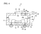
- FIG.4 is a sectional view showing an electronic component device of a second embodiment of the present invention.
- an upper silicon package portion 21 is employed instead of the above upper ceramic package portion 20 of the first embodiment (FIG.2).
- the upper silicon package portion 21 is constructed by an upper frame portion 21a to a center portion of which the opening portion 20x is provided, and an upright frame portion 21b.
- a transparent glass 35 is adhered to the neighboring portion of the opening portion 20x on the outer surface side of the upper silicon package portion 21 with the low-melting glass 26.
- An upper surface of the transparent glass 35 constitutes an inclined surface IS inclined at a desired angle, and a lower surface thereof constitutes a horizontal surface HS.
- the outer surface side of the upper silicon package portion 21 constitutes a horizontal surface that is parallel with the light receiving surface (mounting surface) of the electronic component device.
- the inclined surface IS of the transparent glass 35 may be arranged on the housing portion S side of the package main body 30.
- the package main body 30 is formed of silicon as a whole, the package main body 30 of higher dimensional precision can be obtained.
- the overall package main body 30 is formed of silicon
- individual electronic component devices can be obtained in such a manner that the electronic component is mounted in respective package areas of the silicon wafer on which a plurality of lower silicon package portions 10 are formed, then the silicon wafer on which a plurality of upper silicon package portions 21 are formed is adhered to the above silicon wafer with the low-melting glass 26, and then the silicon wafers are cut into individual pieces. Since such approach is employed, yield in assembling and a production efficiency can be improved, and a lower cost can be achieved.
- the upper package portion formed of silicon (or ceramic, or the like) and not having the opening portion 20x may be employed, in place of the upper silicon package portion 21 in which the opening portion 20x is provided.
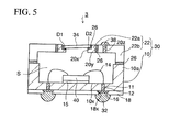
- FIG.5 is a sectional view showing an electronic component device of a third embodiment of the present invention.
- the foregoing electronic component device 1 of the first embodiment (FIG.2)
- the upper ceramic package portion 20 is made of ceramic
- dimensional precision of the upper ceramic package portion 20 cannot be ensured with respect to the lower silicon package portion 10.
- the transparent glass 34 having no inclined surface is provided to the upper silicon package portion 21 to be inclined
- the stepped portions having a different height respectively must be formed on the side surface portion of the opening portion of the silicon, like the case of ceramic.
- the etching step grows complicated to bring about a cost increase.
- an upper package portion 22 of an electronic component device 3 is constructed such that the neighboring portion of the opening portion 20x is formed of a ring-like ceramic portion 22a and a ring-like silicon outer frame portion 22b is adhered to an outer peripheral side surface of the ceramic portion 22a with the low-melting glass 26. Therefore, the transparent glass 34 having no inclined surface can be arranged to be inclined on the stepped portions D1, D2 of the opening portion 20x of the ceramic portion 22a at a low cost. Also, since an outer frame portion of the upper package portion 22 is formed of silicon of high processing precision, dimensional precision of the outer frame portion can be improved rather than the case where the overall upper ceramic package portion 20 is made of ceramic.
- FIG.6 is a sectional view showing an electronic component device of a fourth embodiment of the present invention.
- a thickness of the bottom portion of the lower silicon package portion 10 is set thicker than that of the lower silicon package portion 10 in the first embodiment (FIG.2) to such an extent that enough rigidity can be ensured, and hollow portions 10y are formed locally in portions in which the through electrodes 12 are provided.
- the through hole 11 is provided in a center portion of the hollow portion 10y of the lower silicon package portion 10.
- the through electrodes 12 are filled in the through holes 11.
- the electronic component 40 is connected to the through electrodes 12 that are exposed from bottom portions of the hollow portions 10y of the lower silicon package portion 10, via the wires 14.
- the lower silicon package portion 10 is set to a thickness enough to get sufficient rigidity, and also the hollow portions 10y are provided locally to the portions of the lower silicon package portion 10, in which the through electrodes 12 are provided, to reduce the thickness of those portions. Therefore, the through holes 11 and the through electrodes 12 can be formed easily.
- the upper package portion formed of silicon (or ceramic, or the like) as a whole and having no opening portion may be employed.
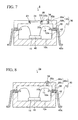
- FIG.7 is a sectional view showing an electronic component device of a fifth embodiment of the present invention.
- an electronic component device 5 of the fifth embodiment no through electrode is provided in the lower silicon package portion 10, and a plurality of leads 42 are adhered with the low-melting glass 26 in a state that they are aligned between the projection portion 10a of the lower silicon package portion 10 and the upright frame portion 20b of the upper ceramic package portion 20.
- Each of the leads 42 extends from the inside of the package main body 30 to the outside.
- the lead 42 being extended outward is arranged to extent and to be bent downward, and an external connection portion 42a is provided in a position that corresponds to the bottom surface of the lower silicon package portion 10.
- the electronic component 40 is connected electrically to the leads 42 of the inside of the package main body 30 via the wires 14.
- FIG.7 In the fifth embodiment (FIG.7), other constituent elements are identical to those in the first embodiment (FIG.2) . Therefore, their explanation will be omitted herein by affixing the same reference symbols to them.
- the upper package portion 20m formed of silicon (or ceramic, or the like) as a whole and having no opening portion 20x is employed.
- a part or all of package main body 30 is formed of silicon. Therefore, the package main body 30 of high dimensional precision can be obtained.
- FIG.9 is a sectional view showing an electronic component device of a sixth embodiment of the present invention.
- opening portions 10z are provided on the outside portion of the area of the lower silicon package portion 10, the area in which the electronic component 40 is mounted, and the leads 42 are arranged below the opening portions 10z.
- the leads 42 are adhered to the outer surface (lower surface) of the lower silicon package portion 10 with the low-melting glass 26 such that internal connection portions 42b are exposed into the opening portions 10z, and the lower surface side of the lead 42 is covered with the low-melting glass 26.
- the leads 42 extend sideward from the outer surface (lower surface) of the lower silicon package portion 10 to the outside, and the external connection portion 42a is provided to the top end portion of the lead 42.
- the electronic component 40 is connected electrically to the internal connection portions 42b of the leads 42 via the wires 14 that pass through the opening portions 10z of the lower silicon package portion 10.
- the opening portions 10z are provided to the lower silicon package portion 10, and the leads 42 are adhered to the lower surface of the lower silicon package portion 10 with the low-melting glass 26 such that the internal connection portions 42b of the leads 42 are arranged in the opening portions 10z. Therefore, unlike the first embodiment, there is no need that the through electrodes 12 should be formed by applying the metal plating to the through holes 11 of the lower silicon package portion 10, and thus the manufacturing method can be simplified.
- the electronic component 40 must be connected to the leads 42 by the wires 14 before the upper ceramic package portion 20 is adhered onto the lower silicon package portion 10 with the low-melting glass 26. Therefore, the electronic component 40 must be connected to the leads 42 in a state that the leads 42 are being fixed by a special fixing jig.
- the electronic component 40 can be connected to the leads 42 via the wires 14 after the leads 42 are secured to the lower surface of the package main body 30 with the low-melting glass 26. Therefore, the electronic component 40 can be mounted by a simple method not to employ the fixing jig fixing the wires 14.
- FIG.9 In the sixth embodiment (FIG.9), other constituent elements are identical to those in the first embodiment (FIG.2) . Therefore, their explanation will be omitted herein by affixing the same reference symbols to them.
- the upper package portion 20m formed of silicon (or ceramic, or the like) as a whole and having no opening portion 20x is employed.
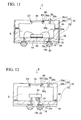
- FIG.11 is a sectional view showing an electronic component device of a seventh embodiment of the present invention.
- the projection portion 10a of the lower silicon package portion 10 and the upright frame portion 20b of the upper ceramic package portion 20 are adhered together by an organic resin 44 such as an epoxy resin, or the like instead of the low-melting glass.
- the electronic component 40 is adhered to the lower silicon package portion 10 by the organic resin 44 instead of the die attachment member.
- the organic resin 44 can be adhered to be cured at a relatively low temperature such as about 200 °C. Therefore, the thermal damage to the electronic component 40 can be reduced rather than the case where the low-melting glass 26 whose curing temperature is 300 to 400 °C is used, and reliability of the electronic component device can be improved.
- the organic resin 44 has a merit of curing on the low temperature side (200 °C), nevertheless its hermetic sealing property for blocking moisture or a gas is not always satisfactory.
- a sealing member 46 made of aluminum, or the like is provided on the side portion of the package main body 30 so as to get the satisfactory hermetic sealing property.
- the organic resin 44 is sealed with the sealing member 46.
- the seventh embodiment can possess the similar advantages to those of the first embodiment. In addition to this, because a temperature in adhering the lower silicon package portion 10 and the upper ceramic package portion 20 can be set low and the satisfactory hermetic sealing property can be obtained, reliability of the electronic component device can be improved.
- FIG.12 is a sectional view showing an electronic component device of an eighth embodiment of the present invention.
- the lower silicon package portion 10 is shaped into a flat plate not to have the recess portion.
- the upright frame portion 20b of the upper ceramic package portion 20 similar to that on the first embodiment is adhered to the peripheral portion of the lower silicon package portion 10 with the low-melting glass 26.
- the through holes 11 are provided in the mounting area of the lower silicon package portion 10, and a projected through electrodes 13 are formed to be filled in the through holes 11.
- the projected through electrodes 13 are arranged to stand upright with a height h from the inner surface of the lower silicon package portion 10.
- the electronic component 40 is mounted to be arranged on the projected through electrodes 13. Then, the electronic component 40 is connected electrically to the projected through electrodes 13 by adhering the connection portions provided to its device surface side to top end portions of the projected through electrodes 13 via a solder, or the like.
- Such electronic component 40 is LED (Light Emitting Diode), for example, and the lower surface side of the electronic component 40 constitutes a device surface (light emitting surface), and light is emitted toward the lower silicon package portion 10 side.
- a mirror, or the like is arranged on the lower silicon package portion 10. The emission light from the electronic component 40 is reflected by the mirror, then is passed through the transparent glass 34, and then is emitted to the outside.
- the eighth embodiment can possess the similar advantages to those of the first embodiment.
- the package of a type that the electronic component device is mounted in the housing portion in a state such the device is separated upward from the lower package portion and is hermetically sealed can be formed with high dimensional precision.
Landscapes
- Solid State Image Pick-Up Elements (AREA)
- Piezo-Electric Or Mechanical Vibrators, Or Delay Or Filter Circuits (AREA)
- Transforming Light Signals Into Electric Signals (AREA)
- Led Device Packages (AREA)
Applications Claiming Priority (1)
| Application Number | Priority Date | Filing Date | Title |
|---|---|---|---|
| JP2006114309A JP2007287967A (ja) | 2006-04-18 | 2006-04-18 | 電子部品装置 |
Publications (2)
| Publication Number | Publication Date |
|---|---|
| EP1848034A2 true EP1848034A2 (fr) | 2007-10-24 |
| EP1848034A3 EP1848034A3 (fr) | 2010-03-10 |
Family
ID=38051805
Family Applications (1)
| Application Number | Title | Priority Date | Filing Date |
|---|---|---|---|
| EP07106386A Withdrawn EP1848034A3 (fr) | 2006-04-18 | 2007-04-18 | Composant électronique |
Country Status (3)
| Country | Link |
|---|---|
| US (1) | US20070241451A1 (fr) |
| EP (1) | EP1848034A3 (fr) |
| JP (1) | JP2007287967A (fr) |
Cited By (5)
| Publication number | Priority date | Publication date | Assignee | Title |
|---|---|---|---|---|
| US20110210026A1 (en) * | 2008-08-25 | 2011-09-01 | Hongzhen Zhao | Shell for electronic device and method of forming the same |
| EP2469613A3 (fr) * | 2010-12-21 | 2013-06-05 | Panasonic Corporation | Dispositif électroluminescent et appareil d'éclairage l'utilisant |
| WO2014087047A1 (fr) * | 2012-12-03 | 2014-06-12 | Lumichip Limited | Composant optoélectronique scellé de manière hermétique |
| DE102016203184A1 (de) * | 2016-02-29 | 2017-05-18 | Conti Temic Microelectronic Gmbh | Leistungselektronikanordnung, Verfahren zur Herstellung einer Leistungselektronikanordnung |
| US12593524B2 (en) | 2019-07-23 | 2026-03-31 | Sony Semiconductor Solutions Corporation | Semiconductor package |
Families Citing this family (17)
| Publication number | Priority date | Publication date | Assignee | Title |
|---|---|---|---|---|
| JP4912275B2 (ja) * | 2007-11-06 | 2012-04-11 | 新光電気工業株式会社 | 半導体パッケージ |
| DE102009004724A1 (de) * | 2009-01-15 | 2010-07-22 | Osram Opto Semiconductors Gmbh | Verfahren zur Herstellung eines optoelektronischen Bauteils und optoelektronisches Bauteil |
| JP2010219377A (ja) * | 2009-03-18 | 2010-09-30 | Toshiba Corp | 半導体発光装置及びその製造方法 |
| US8390083B2 (en) | 2009-09-04 | 2013-03-05 | Analog Devices, Inc. | System with recessed sensing or processing elements |
| JP2011192808A (ja) * | 2010-03-15 | 2011-09-29 | Fujifilm Corp | 撮像モジュール及びその製造方法並びに内視鏡装置 |
| JP5505004B2 (ja) * | 2010-03-17 | 2014-05-28 | 株式会社リコー | 面発光レーザモジュール、光走査装置及び画像形成装置 |
| US9407997B2 (en) | 2010-10-12 | 2016-08-02 | Invensense, Inc. | Microphone package with embedded ASIC |
| JP5845588B2 (ja) * | 2011-02-09 | 2016-01-20 | セイコーエプソン株式会社 | 波長可変干渉フィルター、光モジュール、光分析装置および波長可変干渉フィルターの製造方法 |
| JP6119090B2 (ja) * | 2011-09-27 | 2017-04-26 | セイコーエプソン株式会社 | 光学フィルターデバイス、光学モジュール、及び電子機器 |
| CN104576883B (zh) | 2013-10-29 | 2018-11-16 | 普因特工程有限公司 | 芯片安装用阵列基板及其制造方法 |
| TWI540469B (zh) * | 2014-04-01 | 2016-07-01 | 原相科技股份有限公司 | 高靜電防護之電子裝置 |
| US9666558B2 (en) | 2015-06-29 | 2017-05-30 | Point Engineering Co., Ltd. | Substrate for mounting a chip and chip package using the substrate |
| JP6926408B2 (ja) * | 2016-07-27 | 2021-08-25 | 株式会社リコー | 光スキャナパッケージおよびその製造方法および光走査装置および画像投射装置 |
| JP2019175986A (ja) * | 2018-03-28 | 2019-10-10 | 住友電気工業株式会社 | 光モジュール |
| WO2019208437A1 (fr) * | 2018-04-25 | 2019-10-31 | 京セラ株式会社 | Boîtier de montage d'élément optique, dispositif électronique et module électronique |
| TWI785663B (zh) * | 2020-07-03 | 2022-12-01 | 張菊華 | 感測模組之結構及其製造方法 |
| US11894473B2 (en) * | 2021-09-09 | 2024-02-06 | Chu Hua Chang | Sensing module and manufacturing method thereof |
Family Cites Families (15)
| Publication number | Priority date | Publication date | Assignee | Title |
|---|---|---|---|---|
| US4524238A (en) * | 1982-12-29 | 1985-06-18 | Olin Corporation | Semiconductor packages |
| JPS61105857A (ja) * | 1985-08-07 | 1986-05-23 | Hitachi Ltd | 半導体装置の製造方法 |
| US4870745A (en) * | 1987-12-23 | 1989-10-03 | Siemens-Bendix Automotive Electronics L.P. | Methods of making silicon-based sensors |
| US4888449A (en) * | 1988-01-04 | 1989-12-19 | Olin Corporation | Semiconductor package |
| US4897508A (en) * | 1988-02-10 | 1990-01-30 | Olin Corporation | Metal electronic package |
| US5314458A (en) * | 1990-06-01 | 1994-05-24 | University Of Michigan | Single channel microstimulator |
| NO911774D0 (no) * | 1991-05-06 | 1991-05-06 | Sensonor As | Anordning ved innkapsling av et funksjonsorgan, samt fremgangsmaate for fremstilling av samme. |
| US5543612A (en) * | 1994-05-13 | 1996-08-06 | Texas Instruments Incorporated | Image pickup device with attached interference stripe noise prevention mechanism |
| DE19508222C1 (de) * | 1995-03-08 | 1996-06-05 | Siemens Ag | Optoelektronischer Wandler und Herstellverfahren |
| US5801073A (en) * | 1995-05-25 | 1998-09-01 | Charles Stark Draper Laboratory | Net-shape ceramic processing for electronic devices and packages |
| JPH09222372A (ja) * | 1996-02-19 | 1997-08-26 | Mitsubishi Electric Corp | 半導体式センサ |
| US6314117B1 (en) * | 1998-12-16 | 2001-11-06 | Quan Photonics, Inc | Laser diode package |
| US6759266B1 (en) * | 2001-09-04 | 2004-07-06 | Amkor Technology, Inc. | Quick sealing glass-lidded package fabrication method |
| US6953985B2 (en) * | 2002-06-12 | 2005-10-11 | Freescale Semiconductor, Inc. | Wafer level MEMS packaging |
| US6969204B2 (en) * | 2002-11-26 | 2005-11-29 | Hymite A/S | Optical package with an integrated lens and optical assemblies incorporating the package |
-
2006
- 2006-04-18 JP JP2006114309A patent/JP2007287967A/ja not_active Withdrawn
-
2007
- 2007-04-18 US US11/785,468 patent/US20070241451A1/en not_active Abandoned
- 2007-04-18 EP EP07106386A patent/EP1848034A3/fr not_active Withdrawn
Cited By (6)
| Publication number | Priority date | Publication date | Assignee | Title |
|---|---|---|---|---|
| US20110210026A1 (en) * | 2008-08-25 | 2011-09-01 | Hongzhen Zhao | Shell for electronic device and method of forming the same |
| EP2469613A3 (fr) * | 2010-12-21 | 2013-06-05 | Panasonic Corporation | Dispositif électroluminescent et appareil d'éclairage l'utilisant |
| US8592836B2 (en) | 2010-12-21 | 2013-11-26 | Panasonic Corporation | Light emitting device and illumination apparatus using same |
| WO2014087047A1 (fr) * | 2012-12-03 | 2014-06-12 | Lumichip Limited | Composant optoélectronique scellé de manière hermétique |
| DE102016203184A1 (de) * | 2016-02-29 | 2017-05-18 | Conti Temic Microelectronic Gmbh | Leistungselektronikanordnung, Verfahren zur Herstellung einer Leistungselektronikanordnung |
| US12593524B2 (en) | 2019-07-23 | 2026-03-31 | Sony Semiconductor Solutions Corporation | Semiconductor package |
Also Published As
| Publication number | Publication date |
|---|---|
| JP2007287967A (ja) | 2007-11-01 |
| US20070241451A1 (en) | 2007-10-18 |
| EP1848034A3 (fr) | 2010-03-10 |
Similar Documents
| Publication | Publication Date | Title |
|---|---|---|
| EP1848034A2 (fr) | Composant électronique | |
| US6686588B1 (en) | Optical module with lens integral holder | |
| US7609461B1 (en) | Optical module having cavity substrate | |
| EP1830417B1 (fr) | Dispositif semi-conducteur et son procédé de fabrication | |
| US7494292B2 (en) | Image sensor module structure comprising wire bonding package and method of manufacturing the image sensor module structure | |
| US6734419B1 (en) | Method for forming an image sensor package with vision die in lens housing | |
| US20070166866A1 (en) | Overmolded optical package | |
| US20070029562A1 (en) | Semiconductor device and method of manufacturing a semiconductor device | |
| US7961989B2 (en) | Optical chassis, camera having an optical chassis, and associated methods | |
| CN101569023A (zh) | 用于光电子器件的壳体和光电子器件在壳体中的布置 | |
| KR20040108601A (ko) | 반도체 장치 및 그 제조 방법 | |
| JP2007537670A (ja) | マイクロエレクトロニクスイメージャ用カバー及びマイクロエレクトロニクスイメージャをウェファレベルでパッケージングする方法 | |
| JP7703567B2 (ja) | 半導体側面放射レーザー用の密閉表面実装パッケージ、及びその形成方法 | |
| US6693364B2 (en) | Optical integrated circuit element package and process for making the same | |
| US9309043B2 (en) | Optical element storage package, optical filter device, optical module, and electronic apparatus | |
| CN103797580A (zh) | 用于制造多个光电子器件的方法和光电子器件 | |
| US20140117201A1 (en) | Optical sensing element arrangement with integral package | |
| JP4315833B2 (ja) | 回路装置 | |
| US7307285B2 (en) | Optical semiconductor device and a method for manufacturing the same | |
| US6528857B1 (en) | Chip size image sensor bumped package | |
| TWI777947B (zh) | 光電模組總成及製造方法 | |
| US20070126916A1 (en) | Image sensor chip packaging method | |
| US20200144786A1 (en) | Quad Flat No-leads Package for Side Emitting Laser Diode | |
| EP3687009B1 (fr) | Élément de réception d'élément électroluminescent, élément de réseau et dispositif électroluminescent | |
| JP2006128514A (ja) | 光半導体装置およびそれを用いた光モジュール |
Legal Events
| Date | Code | Title | Description |
|---|---|---|---|
| PUAI | Public reference made under article 153(3) epc to a published international application that has entered the european phase |
Free format text: ORIGINAL CODE: 0009012 |
|
| AK | Designated contracting states |
Kind code of ref document: A2 Designated state(s): AT BE BG CH CY CZ DE DK EE ES FI FR GB GR HU IE IS IT LI LT LU LV MC MT NL PL PT RO SE SI SK TR |
|
| AX | Request for extension of the european patent |
Extension state: AL BA HR MK YU |
|
| PUAL | Search report despatched |
Free format text: ORIGINAL CODE: 0009013 |
|
| AK | Designated contracting states |
Kind code of ref document: A3 Designated state(s): AT BE BG CH CY CZ DE DK EE ES FI FR GB GR HU IE IS IT LI LT LU LV MC MT NL PL PT RO SE SI SK TR |
|
| AX | Request for extension of the european patent |
Extension state: AL BA HR MK RS |
|
| RIC1 | Information provided on ipc code assigned before grant |
Ipc: H01L 23/06 20060101ALI20100129BHEP Ipc: H01L 23/04 20060101ALI20100129BHEP Ipc: H01L 23/14 20060101AFI20070530BHEP |
|
| AKY | No designation fees paid | ||
| REG | Reference to a national code |
Ref country code: DE Ref legal event code: 8566 |
|
| STAA | Information on the status of an ep patent application or granted ep patent |
Free format text: STATUS: THE APPLICATION IS DEEMED TO BE WITHDRAWN |
|
| 18D | Application deemed to be withdrawn |
Effective date: 20100911 |