EP1848112A1 - Automatische Verstärkungssteuerungsschaltung mit Steuerung des Sollwertes - Google Patents
Automatische Verstärkungssteuerungsschaltung mit Steuerung des Sollwertes Download PDFInfo
- Publication number
- EP1848112A1 EP1848112A1 EP07251662A EP07251662A EP1848112A1 EP 1848112 A1 EP1848112 A1 EP 1848112A1 EP 07251662 A EP07251662 A EP 07251662A EP 07251662 A EP07251662 A EP 07251662A EP 1848112 A1 EP1848112 A1 EP 1848112A1
- Authority
- EP
- European Patent Office
- Prior art keywords
- clip
- signal
- automatic gain
- circuit
- target value
- Prior art date
- Legal status (The legal status is an assumption and is not a legal conclusion. Google has not performed a legal analysis and makes no representation as to the accuracy of the status listed.)
- Withdrawn
Links
Images


Classifications
-
- H—ELECTRICITY
- H04—ELECTRIC COMMUNICATION TECHNIQUE
- H04L—TRANSMISSION OF DIGITAL INFORMATION, e.g. TELEGRAPHIC COMMUNICATION
- H04L27/00—Modulated-carrier systems
- H04L27/26—Systems using multi-frequency codes
-
- H—ELECTRICITY
- H03—ELECTRONIC CIRCUITRY
- H03G—CONTROL OF AMPLIFICATION
- H03G3/00—Gain control in amplifiers or frequency changers
- H03G3/20—Automatic control
- H03G3/30—Automatic control in amplifiers having semiconductor devices
- H03G3/3052—Automatic control in amplifiers having semiconductor devices in bandpass amplifiers (H.F. or I.F.) or in frequency-changers used in a (super)heterodyne receiver
- H03G3/3068—Circuits generating control signals for both R.F. and I.F. stages
-
- H—ELECTRICITY
- H03—ELECTRONIC CIRCUITRY
- H03M—CODING; DECODING; CODE CONVERSION IN GENERAL
- H03M1/00—Analogue/digital conversion; Digital/analogue conversion
- H03M1/12—Analogue/digital converters
- H03M1/18—Automatic control for modifying the range of signals the converter can handle, e.g. gain ranging
- H03M1/181—Automatic control for modifying the range of signals the converter can handle, e.g. gain ranging in feedback mode, i.e. by determining the range to be selected from one or more previous digital output values
- H03M1/183—Automatic control for modifying the range of signals the converter can handle, e.g. gain ranging in feedback mode, i.e. by determining the range to be selected from one or more previous digital output values the feedback signal controlling the gain of an amplifier or attenuator preceding the analogue/digital converter
- H03M1/185—Automatic control for modifying the range of signals the converter can handle, e.g. gain ranging in feedback mode, i.e. by determining the range to be selected from one or more previous digital output values the feedback signal controlling the gain of an amplifier or attenuator preceding the analogue/digital converter the determination of the range being based on more than one digital output value, e.g. on a running average, a power estimation or the rate of change
-
- H—ELECTRICITY
- H04—ELECTRIC COMMUNICATION TECHNIQUE
- H04L—TRANSMISSION OF DIGITAL INFORMATION, e.g. TELEGRAPHIC COMMUNICATION
- H04L27/00—Modulated-carrier systems
- H04L27/26—Systems using multi-frequency codes
- H04L27/2601—Multicarrier modulation systems
- H04L27/2647—Arrangements specific to the receiver only
Definitions
- the present invention relates to an orthogonal frequency division multiplexing (OFDM) receiver for receiving and demodulating an OFDM signal and its automatic gain controller circuit.
- OFDM orthogonal frequency division multiplexing
- an OFDM method a modulation method called an orthogonal frequency division multiplexing method (hereinafter referred to as an OFDM method) is known as a method of modulating digital data.
- an OFDM modulation method a number of orthogonal subcarriers is provided in a transmission band, and digital data is assigned to the amplitude and phase of each subcarrier by phase shift keying (PSK) or quadrature amplitude modulation (QAM) to modulate the digital data.
- PSK phase shift keying
- QAM quadrature amplitude modulation
- the OFDM method divides the transmission band by a number of subcarriers, the band per one subcarrier becomes narrower and a modulation speed lowers. However, it has a feature such that a total transmission speed is not different from that of a modulation method of current related art. Since the OFDM method transmits a number of subcarriers in parallel, a symbol speed becomes lower, thereby enabling to shorten a relative time length of a multipath with respect to a time length of a symbol. It has therefore another feature of less susceptibility to multipath interference.
- Still another feature is such that since the OFDM method assigns data to a plurality of subcarriers, a transmission/reception circuit can be realized by using an Inverse Fast Fourier Transform (IFFT) calculation circuit for inverse Fourier transform during modulation and a Fast Fourier Transform (FFT) calculation circuit for Fourier transform during demodulation.
- IFFT Inverse Fast Fourier Transform
- FFT Fast Fourier Transform
- the OFDM method having these features are often applied to terrestrial digital broadcasting which is strongly influenced by multipath interference.
- there are standards such as Digital Video Broadcasting-Terrestrial (DVB-T) and Integrated Services Digital Broadcasting-Terrestrial Sound Broadcasting (ISDB-TSB) (e.g., refer to "Terrestrial Digital Sound Broadcasting Receiver Standards (Desired Specification) ARIB STD-B30, ver. 1.1", Association of Radio Industries and Businesses, executed on May 31, 2001 and revised to 1.1 on March 28, 2001, and "Transmission Method for Terrestrial Digital Sound Broadcasting ARIB STD-B29, ver. 1.1", Association of Radio Industries and Businesses, executed on May 31, 2001 and revised to 1.1 on March 28, 2001.
- a tuner unit connected to an antenna converts an OFDM signal of a desired reception channel into an intermediate frequency (IF) signal which is then supplied to an intermediate frequency amplifier unit.
- the IF signal amplified by the intermediate frequency amplifier unit is converted into a digital signal by an A/D converter circuit, and the digital signal is supplied to a baseband processing unit.
- the baseband processing unit orthogonally demodulates the digitized IF signal to obtain an OFDM time domain signal of the baseband. Only the effective symbol period of the OFDM time domain signal is subjected to FFT to obtain an OFDM frequency domain signal.
- the OFDM frequency domain signal is subjected to differential demodulation of DQPSK or synchronous demodulation of QPSK, 16QAM or 64QAM to obtain a demodulated output of the OFDM signal of the reception channel.
- the baseband processing unit has therein an automatic gain controller (AGC) circuit which maintains constant the level of the intermediate frequency signal to be supplied to the A/D converter circuit by controlling the gain of a voltage controlled variable gain amplifier constituting the intermediate frequency amplifier unit.
- AGC automatic gain controller
- an automatic gain controller circuit 510 of an OFDM receiver 500 of related art includes an absolute value (ABS) circuit 511, a subtractor circuit 512, a sign judgment (SGN) circuit 513, a low-pass filter 514, a rounding process (RND) circuit 515, an accumulator circuit 516, etc.
- ABS absolute value
- SGN sign judgment
- RND rounding process
- the ABS circuit 511 obtains an absolute value of the signal level value of the intermediate frequency signal by removing the sign of the intermediate frequency signal digitized by and supplied from the A/D converter circuit 504.
- the subtractor circuit 512 subtracts a fixed target value from the signal level value of the intermediate frequency signal changed into the absolute signal level by the ABS circuit 511 to detect a signed difference value.
- the SGN circuit 513 judges the sign of the signed difference value detected by the subtractor circuit 512, and supplies a 1-bit sign signal corresponding to the sign of the difference value to the accumulator circuit 516 via the low-pass filter 514 and rounding process (RND) circuit 515.
- the accumulator circuit 516 outputs an accumulation output as an automatic gain controller (AGC) signal.
- AGC automatic gain controller
- the AGC signal output from the automatic gain controller circuit 510 is supplied to a pulse density modulation (PDM) circuit 520 which outputs a PDM signal of a rectangular wave whose density changes with an amplitude of the AGC signal.
- PDM pulse density modulation
- the PDM signal is fed back via a low-pass filter 525 to a control terminal of a voltage controlled variable gain amplifier 503A constituting an intermediate frequency amplifier unit 503.
- the fixed target value is used as one of input parameters, and subtracted from the absolute value of the signal after A/D conversion.
- the sign of the resultant value is converted into a 1-bit signal. This signal is passed through the low-pass filter 514 and accumulated in the accumulator circuit 516 to obtain and output the AGC signal.
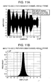
- Input signals to the A/D converter circuit 504 of the OFDM receiver 500 have a property of a Gaussian distribution in an additive white Gaussian noise (AWGN) channel, as shown in Figs. 9A and 9B. If a distribution of input signals is estimated and a fixed target value is used, a clip amount of the input signal can be adjusted. Adjusting noises by clipping and adjusting noises by quantization are properly balanced so that a quantity of noises mixed in the A/D converter circuit 504 can be minimized.
- AWGN additive white Gaussian noise
- the property (distribution) of input signals in a mobile channel to the A/D converter circuit 504 shifts from a Gaussian distribution, as shown in Figs. 10 and 11.
- Figs. 10A and 10B show input signals (without AGC) and their distribution in a flutter channel
- Figs. 11A and 11B show input signals (without AGC) and their distribution in a one-wave Rayleigh channel.
- a target value optimized in an AWGN channel is set, a large quantity of clipping occurs in a mobile channel so that the performance of a receiver is degraded. If a target is set for a mobile channel, quantization noises increases in an AWGN channel so that the performance of a receiver is degraded.
- an orthogonal frequency division multiplexing (OFDM) receiver for receiving and demodulating an OFDM signal without clipping an input signal to an A/D converter circuit in a mobile channel (such as flutter, one-wave Rayleigh) while suppressing degradation.
- OFDM orthogonal frequency division multiplexing
- an automatic gain controller (AGC) circuit of an OFDM receiver automatically controls a target value to an optimum value or substantially optimum value.
- an OFDM receiver for receiving and demodulating an orthogonal frequency division-multiplexing (OFDM) signal.
- the OFDM receiver includes: variable gain amplifier means for controlling a signal level of an intermediate frequency signal that is obtained from a reception signal by frequency-conversion; and an automatic gain controller circuit for controlling a gain of the variable gain amplifier means.
- the automatic gain controller circuit includes: clip detection means for comparing a clip number threshold value with a detected number of transient clips in which a signal level of the intermediate frequency signal that is obtained from a reception signal by frequency-conversion exceeds a parameter clip level, to detect a period where the detected number exceeds the clip number threshold value; accumulator means for accumulating a detection output of the clip detection means; and target value decision means to which an accumulation output of the accumulator means is supplied.
- the target value decision means includes: first comparison means for comparing the accumulation output of the accumulator means with a clip threshold value to judge if a clip occurs; and second comparison means for comparing the accumulation output of the accumulator means with a non-clip threshold value to judge whether clip does not occur.
- a target value for automatic gain control is adaptively determinable by decreasing by a predetermined amount the target value in accordance with a comparison output of the first comparison means and by increasing by a predetermined amount the target value in accordance with a comparison output of the second comparison means.
- an automatic gain controller circuit in an OFDM receiver for receiving and demodulating an orthogonal frequency division-multiplexing (OFDM) signal.
- the automatic gain controller circuit includes: clip detection means for comparing a clip number threshold value with a detected number of transient clips in which a signal level of the intermediate frequency signal that is obtained from a reception signal by frequency-conversion exceeds a parameter clip level, to detect a period where the detected number exceeds the clip number threshold value; accumulator means for accumulating a detection output of the clip detection means; and target value decision means to which an accumulation output of the accumulator means is suppliable.
- the target value decision means includes: first comparison means for comparing the accumulation output of the accumulator means with a clip threshold value to judge if a clip occurs; and second comparison means for comparing the accumulation output of the accumulator means with a non-clip threshold value to judge whether clip does not occur.
- a target value for automatic gain control is adaptively determined by decreasing by a predetermined amount the target value in accordance with a comparison output of the first comparison means and by increasing by a predetermined amount the target value in accordance with a comparison output of the second comparison means.
- the automatic gain controller (AGC) circuit of an OFDM receiver automatically controls a target value to an optimum value or a substantially optimum value. It is therefore possible not to clip an input signal for an A/D converter circuit in a mobile channel (such as flutter, one-wave Rayleigh), thereby suppressing degradation.
- the OFDM receiver 100 includes a tuner unit 102 connected to an antenna 101, an intermediate frequency amplifier unit 103 to which an intermediate frequency (IF) signal converted from an OFDM signal of a desired reception channel by the tuner unit 102 is input, a baseband processing unit 105 to which the intermediate frequency signal amplified by the intermediate frequency amplifier unit 103 and digitized by an A/D converter circuit 104 is input, etc.
- IF intermediate frequency
- the baseband processing unit 105 orthogonally demodulates the digitized IF signal and obtains an OFDM time domain signal of the baseband.
- the OFDM frequency domain signal is subjected to differential demodulation of DQPSK or synchronous demodulation of QPSK, 16QAM or 64QAM to obtain a demodulated output of the OFDM signal of the reception channel.
- the baseband processing unit 105 contains therein an automatic gain controller (AGC) circuit 110 which maintains constant the level of the intermediate IF signal to be supplied to the A/D converter circuit 104, by controlling the gain of a voltage controlled variable gain amplifier constituting the intermediate frequency amplifier unit 103.
- AGC automatic gain controller
- the automatic gain controller circuit 10 may include an absolute value (ABS) circuit 11, a subtractor circuit 12, an automatic target circuit 13, a sign judgment (SGN) circuit 14, a low-pass filter 15, a rounding process (RND) circuit 16, an accumulator circuit 17, etc.
- ABS absolute value
- SGN sign judgment
- RTD rounding process
- the ABS circuit 11 obtains an absolute value of the signal level value of the intermediate frequency signal by removing the sign of the intermediate frequency signal digitized by and supplied from the A/D converter circuit 104.
- the subtractor circuit 12 subtracts a target value supplied from the automatic target circuit 13 from the signal level value of the intermediate frequency signal changed into the absolute value by the ABS circuit 11 to detect a signed difference value.
- the SGN circuit 14 judges the sign of the signed difference value detected by the subtractor circuit 12, and supplies a 1-bit sign signal corresponding to the sign of the difference value to the accumulator circuit 17 via the low-pass filter 15 and rounding process (RND) circuit 16.
- the accumulator circuit 17 accumulates the sign signal supplied via the rounding process (RND) circuit 16 and outputs an accumulation output as an automatic gain controller (AGC) signal.
- AGC automatic gain controller
- the AGC signal output from the automatic gain controller circuit 10 is supplied to a pulse density modulation (PDM) circuit 120 which outputs a PDM signal of a rectangular wave whose density changes with an amplitude of the AGC signal.
- PDM pulse density modulation
- the PDM signal is fed back via a low-pass filter 125 to a control terminal of a voltage controlled variable gain amplifier 103A constituting an intermediate frequency amplifier unit 103.
- the automatic target circuit 13 may include a clip detection circuit 131 to which the signal level value of the intermediate frequency signal changed to the absolute value by the ABS circuit 11 is input, an accumulator circuit 132 for accumulating a detection output from the clip detection circuit 131, and a target value decision circuit 133 to which an accumulation value from the accumulator circuit 132 is input.
- the clip detection circuit 131 may include a clip level comparator 311, an adder 312, a register 313 and a clip number comparator 314.
- the clip level comparator 311 compares a parameter clip level with the signal level value of the intermediate frequency signal changed to the absolute value by and supplied from the ABS circuit 11, and if the signal level value is larger, detects it as a transient clip.
- the register 313 is cleared at a predetermined period to store a cumulative addition value of the detected number of transient clips.
- the clip number comparator 314 compares a clip number threshold value with the detected number of transient clips stored in the register 313. If the detected number is equal to the clip threshold value or more, it is judged that a clip occurs during the corresponding period, and "1" is output as a clip detection. If the detected number is smaller than the threshold value, "0" is output.
- the accumulator circuit 132 of the automatic target circuit 13 accumulates the detection output of the clip detection circuit 131, and inputs the accumulation output to the target value decision circuit 133.
- the detection output of the clip detection circuit 131 may be input directly to the target value decision circuit 133. However, in order to monitor the signal level value in a longer period for dealing with slow fading, the detection output of the clip detection circuit 131 of the automatic target circuit is accumulated during a predetermined accumulation period by the accumulator circuit 132, and the accumulation output is input to the target value decision circuit 133.
- the target value decision circuit 133 includes first and second comparators 331 and 332, a near-clip state detection circuit 333, a subtractor 334, an adder 335, first and second data selectors 336 and 337, an AND gate 338, a register 339, etc.
- the accumulation output of the accumulator circuit 13 is input to the first and second comparators 331, 332 and to the near-clip state detection circuit 333.
- the first comparator 331 is supplied with a clip threshold value SH1 for determining that the clip occurs
- the second comparator 332 is supplied with a non-clip threshold value SH2 for determining that the clip does not occur.
- the near-clip state detection circuit 333 is supplied with a near-clip threshold value SH3 for determining that the state is a near-clip state.
- the register 339 is supplied with a target initial value TG0.
- the target value output from the resister 339 is supplied to the subtractor 334 and first and second data selectors 336 and 337.
- the subtractor 334 is supplied with subtraction data DD indicating an amount for decreasing the target value
- the adder 335 is supplied with addition data DI indicating an amount for increasing the target value.
- the subtractor 334 subtracts the amount for decreasing the target value represented by the subtraction data DD from the target value TG output from the register 339, and inputs a substraction output to the first data selector 336.
- the adder 335 adds the amount for increasing the target value represented by the addition data DI to the selection output by the first data selector 336, and inputs an addition output to the second data selector 337.
- the first comparator 331 compares the accumulation output of the accumulator circuit 13 with the clip threshold value SH1, which is the value for determining that the clip occurs, and controls the first data selector 336 by the comparison output.
- the first data selector 336 selects the substraction output from the register 339 if the accumulation output of the accumulator circuit 13 exceeds the clip threshold value SH1.
- the subtraction output is obtained by subtracting the amount for decreasing the target value, which is obtained by the subtractor 334, from the target value TG If the accumulation output of the accumulator circuit 13 does not exceed the clip threshold value SH2, which is the value for determining that the clip does not occur, the first selector 336 selects the target value TG output from the resister 339. In this way, if the clip occurs, the target value TG is lowered.
- a selection output by the first data selector 336 is input to the adder 335 and the second data selector 337.
- the second comparator 332 compares the accumulation output of the accumulator circuit 13 with the non-clip threshold value SH2, which is the value for determining that the clip does not occur, and controls the second data selector 337 by the comparison output via the AND gate 338.
- the near-clip state detection circuit 333 detects the near-clip state, which is close but not equal to the clip-state, based on an accumulation output of the accumulator circuit 13 and the near-clip threshold value SH3, which is the value for determining the near-clip state.
- the second data selector 337 selects the addition output if the accumulation output of the accumulator circuit 13 does not exceed the clip threshold value SH2, which is the value for determining that the clip does not occur.
- the addition output is obtained by adding the amount for increasing the target value output from the adder 335 to the selection output of the first data selector 336. If the accumulation output of the accumulator circuit 13 exceeds the clip threshold value SH2, the second selector 337 selects the selection output of the first data selector 336. In this way, if the clip does not occur, the target value TG is increased.
- a selection output by the second data selector 337 is input to the register 339.
- the amount for increasing or decreasing the target value may be an external parameter (amount for increasing or decreasing the target value) or a fixed value.
- the near-clip state detection circuit 333 detects the near-clip state that is close but not equal to the clip state, and upon the near-clip state detection, the target value will not be increased.
- the near-clip state detection circuit 333 may be a circuit which, for example, subtracts "1" from an output of the accumulator circuit 132 and compares the subtraction result with the near-clip threshold value. The near-clip state detection circuit 132 further outputs "1" if the subtraction result is larger.
- the automatic gain controller circuit 10 having the structure described above may deal with the clip which occurs over a longer span of time, by having the automatic target circuit 13.
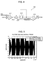
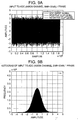
- the clip may occur with a shorter time period. Particularly at a flutter channel of 0 dB, a signal may disappear repetitively. In this case, a typical automatic gain control increases the gain greatly, and the clip occurs as shown in Fig. 5.
- the OFDM receiver 100 used in the reception environment of this kind may use an automatic gain control circuit 20 having the structure such as shown in Fig. 6, in place of the above-described automatic gain controller circuit 10.
- the automatic gain controller circuit 20 shown in Fig. 6 is an improved version of the automatic gain control circuit 10 to prevent the clip from occurring within a shorter time period.
- the automatic gain controller circuit 20 includes an absolute value (ABS) circuit 21, a subtractor circuit 22, an automatic target circuit 23, a sign (SGN) judgment circuit 24, a low-pass filter 25, a rounding process (RND) circuit 26, an accumulator circuit 27, a signal-off detection circuit 28, a clip detection circuit 29, etc.
- the absolute value (ABS) circuit 21, the subtractor circuit 22, the automatic target circuit 23, the sign (SGN) judgment circuit 24, the low-pass filter 25, the rounding process (RND) circuit 26, and the accumulator circuit 27 respectively of the automatic gain controller circuit 20 correspond to the absolute value (ABS) circuit 11, the subtractor circuit 12, the automatic target circuit 13, the sign (SGN) judgment circuit 14, the low-pass filter 15, the rounding process (RND) circuit 16, and the accumulator circuit 17 respectively of the automatic gain controller circuit 10, and the description of the constituent elements other than the low-pass filter 25 is omitted.
- the low-pass filter 25 has an adder circuit 251 to which a 1-bit sign signal is supplied from the SGN circuit 24, a register 252 for storing an addition output value of the adder circuit 251, a weighting circuit 253 for weighting an addition output value of the adder circuit 251 by (1- ⁇ ), and a bit shift circuit 254 to which supplied is the addition output value of the adder circuit 251 stored in the register 252.
- the addition output value of the adder circuit 251 stored in the register 252 is supplied back to the adder circuit 251 via the weighting circuit 253.
- the low-pass filter 25 functions as a low-pass filter such that the adder circuit 251 conducts cumulative addition of the sign signal supplied from the SGN circuit 14 and weighted by (1- ⁇ ) by the weighting circuit 253.
- the low-pass filter can change its pass-band width by controlling the bit shift circuit 254 which generates and outputs an AGC control signal.
- the AGC control signal is the addition output value of the adder circuit 251 stored in the register 252 and attenuated by 1/2 n through n-bit shift.
- the signal-off detection circuit 28 includes a signal-off level comparator 281, an adder 282, a resister 283 and a signal-off number comparator 284.
- the signal-off level comparator 281 compares a signal-off level with the signal level value of the intermediate frequency signal that is changed to the absolute value by and supplied from the ABS circuit 21, and detects a state of a signal-off if the signal level value is smaller.
- An output of the signal-off level comparator i.e., a detection output of signal-off, is added to the detected number of signal-off stored in the register 283 by the adder 282.
- the register 283 is cleared at a predetermined period and stores a cumulative addition value of the detected number of signal-off.
- the signal-off comparator 284 compares a signal-off number threshold value with the detected number of signal-off stored in the register 283.
- the signal-off detection circuit 28 outputs a signal-off detection signal which represents by "1” the period where the signal-off detected number exceeds the signal-off threshold value and by "0" the period where the signal-off detected number is smaller than the threshold value.
- the clip detection circuit 29 is structured similar to the clip detection circuit 131 shown in Fig. 4.
- the clip detection circuit outputs the clip detection signal which represents by "1" the period where a detected number of transient clips in which the signal level value of the intermediate frequency signal, which is changed to the absolute value by and supplied from the ABS circuit 21, exceeds the clip number threshold value, and represents by "0" the period in which the detected number is smaller than the threshold value.
- the operation of the bit shift circuit 254 is controlled by each detection output of the signal-off detection circuit 28 and the clip detection circuit 29.
- a bit shift amount n of the bit shift circuit 254 is increased. In this way, in the signal-off state, a change amount of the AGC control signal is reduced so as to narrow the pass-band width, and to increase the gain of an output of the automatic gain controller circuit 20 by a small amount.
- the bit shift amount n of the bit shift circuit 254 is reduced. In this way, when the clip occurs, the change amount of the AGC control signal is increased immediately so as to broaden the pass-band width, and to lower the output gain quickly.
- the target level of AGC is changed at the mobile channel (particularly flutter channel) so as to reduce the clip of an AGC input signal, thereby enabling improvement of characteristics of a receiver at a succeeding stage.
- the clip state can be reduced, thereby enabling improvement of characteristics of a receiver at a succeeding stage.
- the clip caused by having ACI, CCI and other noised mixed in an OFDM signal can be reduced, thereby enabling improvement of characteristics of a receiver at a succeeding stage.
Landscapes
- Engineering & Computer Science (AREA)
- Theoretical Computer Science (AREA)
- Computer Networks & Wireless Communication (AREA)
- Signal Processing (AREA)
- Control Of Amplification And Gain Control (AREA)
- Circuits Of Receivers In General (AREA)
Applications Claiming Priority (1)
| Application Number | Priority Date | Filing Date | Title |
|---|---|---|---|
| JP2006118319A JP4211802B2 (ja) | 2006-04-21 | 2006-04-21 | Ofdm受信装置及びその自動利得制御回路 |
Publications (1)
| Publication Number | Publication Date |
|---|---|
| EP1848112A1 true EP1848112A1 (de) | 2007-10-24 |
Family
ID=38331134
Family Applications (1)
| Application Number | Title | Priority Date | Filing Date |
|---|---|---|---|
| EP07251662A Withdrawn EP1848112A1 (de) | 2006-04-21 | 2007-04-20 | Automatische Verstärkungssteuerungsschaltung mit Steuerung des Sollwertes |
Country Status (5)
| Country | Link |
|---|---|
| US (1) | US8045659B2 (de) |
| EP (1) | EP1848112A1 (de) |
| JP (1) | JP4211802B2 (de) |
| KR (1) | KR101316643B1 (de) |
| CN (1) | CN101060516A (de) |
Cited By (1)
| Publication number | Priority date | Publication date | Assignee | Title |
|---|---|---|---|---|
| CN101964774A (zh) * | 2010-10-14 | 2011-02-02 | 信源通科技(西安)有限公司 | 一种适用于ofdm系统的自动增益控制方法及控制电路 |
Families Citing this family (10)
| Publication number | Priority date | Publication date | Assignee | Title |
|---|---|---|---|---|
| US20090059782A1 (en) * | 2007-08-29 | 2009-03-05 | Rgb Systems, Inc. | Method and apparatus for extending the transmission capability of twisted pair communication systems |
| CN102291343B (zh) * | 2011-08-08 | 2016-12-28 | 上海集成电路研发中心有限公司 | 模拟基带电路 |
| US9746385B2 (en) * | 2013-06-12 | 2017-08-29 | Honeywell International Inc. | System and method for measuring varying parameters using adaptive signal conditioning |
| CN106527121A (zh) * | 2016-12-20 | 2017-03-22 | 上海华林工业气体有限公司 | 一种带有限幅器的pid控制装置及方法 |
| WO2018120072A1 (en) * | 2016-12-30 | 2018-07-05 | Texas Instruments Incorporated | Total harmonic distortion (thd) controlled clip detector and automatic gain limiter (agl) |
| JP7004503B2 (ja) * | 2017-01-27 | 2022-01-21 | ラピスセミコンダクタ株式会社 | 自動利得制御回路(agc)、逆拡散回路及び受信データの再生方法 |
| CN110098880A (zh) * | 2019-04-25 | 2019-08-06 | 浙江大学 | 一种无人机射频信号功率多通道并行检测装置 |
| JP7778707B2 (ja) * | 2020-09-16 | 2025-12-02 | ソニーセミコンダクタソリューションズ株式会社 | 信号処理装置、信号処理方法、及び、受信装置 |
| CN114421981B (zh) * | 2021-12-14 | 2023-09-22 | 江苏芯云电子科技有限公司 | 一种脉冲噪声滤波装置及方法 |
| US12483216B2 (en) | 2022-07-27 | 2025-11-25 | Crystal Instruments Corporation | Data recording based on dual ADC architecture |
Citations (9)
| Publication number | Priority date | Publication date | Assignee | Title |
|---|---|---|---|---|
| US5563916A (en) * | 1995-06-05 | 1996-10-08 | Hitachi America, Ltd. | Apparatus and method for varying the slew rate of a digital automatic gain control circuit |
| US6081565A (en) * | 1998-02-05 | 2000-06-27 | Lucent Technologies Inc. | Amplitude based coarse automatic gain control circuit |
| EP1061653A2 (de) * | 1999-06-18 | 2000-12-20 | Nortel Networks Limited | Einstellung einer analogen Verstärkungsregelung mit Hilfe eines probabilistischen Algorithmus |
| US6292120B1 (en) * | 2000-03-02 | 2001-09-18 | Adc Telecommunications, Inc. | Automatic gain control for input to analog to digital converter |
| GB2369258A (en) * | 2000-11-21 | 2002-05-22 | Ubinetics Ltd | A radio receiver wherein a gain is reduced by two steps when a predetermined level of ADC saturation is reached |
| US20030194029A1 (en) * | 1999-06-23 | 2003-10-16 | Heinonen Jari M. | Automatic gain control methods and apparatus suitable for use in OFDM receivers |
| EP1363403A1 (de) * | 2002-05-16 | 2003-11-19 | Sony International (Europe) GmbH | Empfangsvorrichtung mit automatischer Verstärkungsregelung |
| US6668027B1 (en) * | 1999-03-02 | 2003-12-23 | Hitachi America, Ltd. | Self adjusting automatic gain control (AGC) power reference level circuit |
| EP1439636A1 (de) * | 2003-01-08 | 2004-07-21 | Agilent Technologies, Inc., a corporation of the State of Delaware | Verfahren zur automatischen verstärkungsregelung |
Family Cites Families (1)
| Publication number | Priority date | Publication date | Assignee | Title |
|---|---|---|---|---|
| JP3183078B2 (ja) * | 1994-02-28 | 2001-07-03 | 三菱電機株式会社 | 制御信号生成回路、これを用いた自動利得制御回路、これを用いた受信機及びこれを用いた通信システム |
-
2006
- 2006-04-21 JP JP2006118319A patent/JP4211802B2/ja not_active Expired - Fee Related
-
2007
- 2007-04-18 KR KR1020070037808A patent/KR101316643B1/ko not_active Expired - Fee Related
- 2007-04-19 US US11/737,546 patent/US8045659B2/en not_active Expired - Fee Related
- 2007-04-20 CN CNA2007100982414A patent/CN101060516A/zh active Pending
- 2007-04-20 EP EP07251662A patent/EP1848112A1/de not_active Withdrawn
Patent Citations (9)
| Publication number | Priority date | Publication date | Assignee | Title |
|---|---|---|---|---|
| US5563916A (en) * | 1995-06-05 | 1996-10-08 | Hitachi America, Ltd. | Apparatus and method for varying the slew rate of a digital automatic gain control circuit |
| US6081565A (en) * | 1998-02-05 | 2000-06-27 | Lucent Technologies Inc. | Amplitude based coarse automatic gain control circuit |
| US6668027B1 (en) * | 1999-03-02 | 2003-12-23 | Hitachi America, Ltd. | Self adjusting automatic gain control (AGC) power reference level circuit |
| EP1061653A2 (de) * | 1999-06-18 | 2000-12-20 | Nortel Networks Limited | Einstellung einer analogen Verstärkungsregelung mit Hilfe eines probabilistischen Algorithmus |
| US20030194029A1 (en) * | 1999-06-23 | 2003-10-16 | Heinonen Jari M. | Automatic gain control methods and apparatus suitable for use in OFDM receivers |
| US6292120B1 (en) * | 2000-03-02 | 2001-09-18 | Adc Telecommunications, Inc. | Automatic gain control for input to analog to digital converter |
| GB2369258A (en) * | 2000-11-21 | 2002-05-22 | Ubinetics Ltd | A radio receiver wherein a gain is reduced by two steps when a predetermined level of ADC saturation is reached |
| EP1363403A1 (de) * | 2002-05-16 | 2003-11-19 | Sony International (Europe) GmbH | Empfangsvorrichtung mit automatischer Verstärkungsregelung |
| EP1439636A1 (de) * | 2003-01-08 | 2004-07-21 | Agilent Technologies, Inc., a corporation of the State of Delaware | Verfahren zur automatischen verstärkungsregelung |
Cited By (2)
| Publication number | Priority date | Publication date | Assignee | Title |
|---|---|---|---|---|
| CN101964774A (zh) * | 2010-10-14 | 2011-02-02 | 信源通科技(西安)有限公司 | 一种适用于ofdm系统的自动增益控制方法及控制电路 |
| CN101964774B (zh) * | 2010-10-14 | 2013-09-18 | 信源通科技(西安)有限公司 | 一种适用于ofdm系统的自动增益控制方法及控制电路 |
Also Published As
| Publication number | Publication date |
|---|---|
| US20070248177A1 (en) | 2007-10-25 |
| CN101060516A (zh) | 2007-10-24 |
| JP2007295111A (ja) | 2007-11-08 |
| KR101316643B1 (ko) | 2013-10-18 |
| KR20070104243A (ko) | 2007-10-25 |
| US8045659B2 (en) | 2011-10-25 |
| JP4211802B2 (ja) | 2009-01-21 |
Similar Documents
| Publication | Publication Date | Title |
|---|---|---|
| US8045659B2 (en) | OFDM receiver and its automatic gain control circuit | |
| JP4749501B2 (ja) | Ofdm受信装置 | |
| US7519122B2 (en) | OFDM reception apparatus and OFDM reception method | |
| KR101061742B1 (ko) | 무선 통신을 위한 재머 검출 및 억제 | |
| US7664189B2 (en) | OFDM demodulator, receiver, and method | |
| JP5988527B2 (ja) | 受信装置 | |
| KR101095326B1 (ko) | Ofdm 변조된 물리 채널에서의 아날로그 이득 스위칭의 위상 보상 | |
| CN1305277A (zh) | 正交频分多路复用分集式接收机 | |
| US9118514B2 (en) | Receiver and signal processing method | |
| US8391423B2 (en) | Estimating method for maximum channel delay and cyclic prefix (CP) averaging method in OFDM receiver | |
| JP2001127732A (ja) | 受信装置 | |
| JPWO2007091562A1 (ja) | 復調装置、方法及びプログラム | |
| JP4287691B2 (ja) | Ofdm受信装置 | |
| JP2005236666A (ja) | Ofdm復調装置 | |
| JP5110586B2 (ja) | Ofdm復調装置、ofdm復調方法、ofdm復調プログラムおよびそのプログラムを記録した記録媒体 | |
| JP2008283588A (ja) | 受信装置及び受信信号増幅率設定方法 | |
| JP2007027879A (ja) | 受信装置および受信方法 | |
| JP2010041627A (ja) | 受信方法および装置 | |
| JP2003304182A (ja) | ダイバーシティ受信機 | |
| JP5128434B2 (ja) | 復調装置、復調方法、復調制御プログラム、および記録媒体 | |
| JP2013031158A (ja) | Ofdm方式における自動利得制御回路及び自動利得制御方法 |
Legal Events
| Date | Code | Title | Description |
|---|---|---|---|
| PUAI | Public reference made under article 153(3) epc to a published international application that has entered the european phase |
Free format text: ORIGINAL CODE: 0009012 |
|
| 17P | Request for examination filed |
Effective date: 20070502 |
|
| AK | Designated contracting states |
Kind code of ref document: A1 Designated state(s): AT BE BG CH CY CZ DE DK EE ES FI FR GB GR HU IE IS IT LI LT LU LV MC MT NL PL PT RO SE SI SK TR |
|
| AX | Request for extension of the european patent |
Extension state: AL BA HR MK YU |
|
| 17Q | First examination report despatched |
Effective date: 20080514 |
|
| AKX | Designation fees paid |
Designated state(s): DE FR GB |
|
| STAA | Information on the status of an ep patent application or granted ep patent |
Free format text: STATUS: EXAMINATION IS IN PROGRESS |
|
| STAA | Information on the status of an ep patent application or granted ep patent |
Free format text: STATUS: THE APPLICATION IS DEEMED TO BE WITHDRAWN |
|
| 18D | Application deemed to be withdrawn |
Effective date: 20171103 |