EP1848128B1 - Dispositif de communication optique et système de distribution clé l'utilisant - Google Patents
Dispositif de communication optique et système de distribution clé l'utilisant Download PDFInfo
- Publication number
- EP1848128B1 EP1848128B1 EP07090078A EP07090078A EP1848128B1 EP 1848128 B1 EP1848128 B1 EP 1848128B1 EP 07090078 A EP07090078 A EP 07090078A EP 07090078 A EP07090078 A EP 07090078A EP 1848128 B1 EP1848128 B1 EP 1848128B1
- Authority
- EP
- European Patent Office
- Prior art keywords
- optical
- intensity
- modulator
- modulation
- phase
- Prior art date
- Legal status (The legal status is an assumption and is not a legal conclusion. Google has not performed a legal analysis and makes no representation as to the accuracy of the status listed.)
- Not-in-force
Links
- 230000003287 optical effect Effects 0.000 title claims description 292
- 238000004891 communication Methods 0.000 title claims description 49
- 230000010287 polarization Effects 0.000 claims description 28
- 238000000034 method Methods 0.000 claims description 24
- 238000004590 computer program Methods 0.000 claims 1
- 230000005540 biological transmission Effects 0.000 description 39
- 238000010586 diagram Methods 0.000 description 33
- 102100039643 Rho-related GTP-binding protein Rho6 Human genes 0.000 description 15
- 101710199571 Rho-related GTP-binding protein Rho6 Proteins 0.000 description 15
- 102100039642 Rho-related GTP-binding protein RhoN Human genes 0.000 description 13
- 108050007497 Rho-related GTP-binding protein RhoN Proteins 0.000 description 13
- 239000013307 optical fiber Substances 0.000 description 10
- 230000010363 phase shift Effects 0.000 description 8
- 102100039640 Rho-related GTP-binding protein RhoE Human genes 0.000 description 7
- 108050007494 Rho-related GTP-binding protein RhoE Proteins 0.000 description 7
- 230000008033 biological extinction Effects 0.000 description 7
- 238000005516 engineering process Methods 0.000 description 7
- 238000013461 design Methods 0.000 description 5
- 239000006185 dispersion Substances 0.000 description 5
- 238000012545 processing Methods 0.000 description 5
- 101150098161 APD1 gene Proteins 0.000 description 3
- 230000015556 catabolic process Effects 0.000 description 3
- 238000006243 chemical reaction Methods 0.000 description 3
- 230000001427 coherent effect Effects 0.000 description 3
- 238000006731 degradation reaction Methods 0.000 description 3
- 238000013459 approach Methods 0.000 description 2
- 238000001514 detection method Methods 0.000 description 2
- 230000006866 deterioration Effects 0.000 description 2
- 230000000694 effects Effects 0.000 description 2
- 238000007429 general method Methods 0.000 description 2
- 230000001902 propagating effect Effects 0.000 description 2
- 238000012552 review Methods 0.000 description 2
- 238000001228 spectrum Methods 0.000 description 2
- 230000002123 temporal effect Effects 0.000 description 2
- 229910000980 Aluminium gallium arsenide Inorganic materials 0.000 description 1
- 229910001218 Gallium arsenide Inorganic materials 0.000 description 1
- 229910003327 LiNbO3 Inorganic materials 0.000 description 1
- 230000003321 amplification Effects 0.000 description 1
- 230000007423 decrease Effects 0.000 description 1
- 230000002708 enhancing effect Effects 0.000 description 1
- 230000001747 exhibiting effect Effects 0.000 description 1
- 238000002474 experimental method Methods 0.000 description 1
- 239000000835 fiber Substances 0.000 description 1
- 238000003780 insertion Methods 0.000 description 1
- 230000037431 insertion Effects 0.000 description 1
- 230000010354 integration Effects 0.000 description 1
- 238000012544 monitoring process Methods 0.000 description 1
- 238000003199 nucleic acid amplification method Methods 0.000 description 1
- 238000011160 research Methods 0.000 description 1
- 238000010079 rubber tapping Methods 0.000 description 1
- 230000008054 signal transmission Effects 0.000 description 1
- 230000002269 spontaneous effect Effects 0.000 description 1
Images







Classifications
-
- H—ELECTRICITY
- H04—ELECTRIC COMMUNICATION TECHNIQUE
- H04B—TRANSMISSION
- H04B10/00—Transmission systems employing electromagnetic waves other than radio-waves, e.g. infrared, visible or ultraviolet light, or employing corpuscular radiation, e.g. quantum communication
- H04B10/50—Transmitters
- H04B10/501—Structural aspects
- H04B10/503—Laser transmitters
- H04B10/505—Laser transmitters using external modulation
- H04B10/5051—Laser transmitters using external modulation using a series, i.e. cascade, combination of modulators
-
- H—ELECTRICITY
- H04—ELECTRIC COMMUNICATION TECHNIQUE
- H04B—TRANSMISSION
- H04B10/00—Transmission systems employing electromagnetic waves other than radio-waves, e.g. infrared, visible or ultraviolet light, or employing corpuscular radiation, e.g. quantum communication
- H04B10/50—Transmitters
- H04B10/501—Structural aspects
- H04B10/503—Laser transmitters
- H04B10/505—Laser transmitters using external modulation
-
- H—ELECTRICITY
- H04—ELECTRIC COMMUNICATION TECHNIQUE
- H04B—TRANSMISSION
- H04B10/00—Transmission systems employing electromagnetic waves other than radio-waves, e.g. infrared, visible or ultraviolet light, or employing corpuscular radiation, e.g. quantum communication
- H04B10/50—Transmitters
- H04B10/516—Details of coding or modulation
- H04B10/54—Intensity modulation
-
- H—ELECTRICITY
- H04—ELECTRIC COMMUNICATION TECHNIQUE
- H04B—TRANSMISSION
- H04B10/00—Transmission systems employing electromagnetic waves other than radio-waves, e.g. infrared, visible or ultraviolet light, or employing corpuscular radiation, e.g. quantum communication
- H04B10/50—Transmitters
- H04B10/516—Details of coding or modulation
- H04B10/548—Phase or frequency modulation
-
- H—ELECTRICITY
- H04—ELECTRIC COMMUNICATION TECHNIQUE
- H04B—TRANSMISSION
- H04B10/00—Transmission systems employing electromagnetic waves other than radio-waves, e.g. infrared, visible or ultraviolet light, or employing corpuscular radiation, e.g. quantum communication
- H04B10/70—Photonic quantum communication
-
- H—ELECTRICITY
- H04—ELECTRIC COMMUNICATION TECHNIQUE
- H04L—TRANSMISSION OF DIGITAL INFORMATION, e.g. TELEGRAPHIC COMMUNICATION
- H04L9/00—Cryptographic mechanisms or cryptographic arrangements for secret or secure communications; Network security protocols
- H04L9/08—Key distribution or management, e.g. generation, sharing or updating, of cryptographic keys or passwords
- H04L9/0816—Key establishment, i.e. cryptographic processes or cryptographic protocols whereby a shared secret becomes available to two or more parties, for subsequent use
- H04L9/0852—Quantum cryptography
- H04L9/0858—Details about key distillation or coding, e.g. reconciliation, error correction, privacy amplification, polarisation coding or phase coding
Definitions
- the present invention relates to an optical communication system and, more particularly, to an optical communication apparatus that modulates the intensity and phase of an optical signal to be transmitted, as well as to a quantum key distribution system using the optical communication apparatus.
- the wavelength dispersion is a phenomenon that a propagation delay occurring in a transmission line varies depending on the wavelength of signal light. Since a signal-light spectrum has a specific range of wavelengths, a short-wavelength component and a long-wavelength component of the same signal light accumulate different wavelength dispersion values during propagation. This accumulated dispersion after propagation results in a difference in propagation delay, that is, causes waveform distortion. On comparison using an ASK signal, since the signal-light spectrum changes in proportion to the modulation rate, the waveform distortion due to wavelength dispersion becomes greater proportionately as the data transmission speed rises.
- multiple digital bits per symbol may be employed by modulating both the intensity and phase of light (APSK: Amplitude Phase Shift Keying), which is described in the following papers:
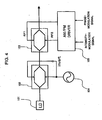
- FIG. 1 is a block diagram showing a schematic configuration of a transmitter that generates an APSK signal, described in S. Hayase et al.
- a light source 1401 generates continuous wave (CW) light, which is subjected at a first-stage Mach-Zehnder (MZ) modulator 1402 to binary phase shift keying (PSK) with two phases of 0 and ⁇ , and is subsequently subjected at a second-stage phase modulator 1403 to binary PSK with two phases of 0 and ⁇ /2.
- MZ Mach-Zehnder
- PSK binary phase shift keying
- a MZ modulator 1404 performs two-level modulation also in the intensity direction on the four-state PSK signal, thereby generating an eight-state (3 bits/symbol) APSK signal. Furthermore, in this example, a MZ modulator 1405 is also used to return to zero (RZ) each bit.
- a multivalued signal such as the APSK signal has an increased number of states per symbol on the one hand, but has a reduced distance between signal points on I-Q plane on the other hand. Therefore, if an attempt is made to obtain the same code error rate as that achieved by a binary modulation scheme such as ASK or BPSK, a large carrier-to-noise ratio (CNR) is needed.
- CNR carrier-to-noise ratio
- QKD quantum key distribution
- photons are generally used as a communication medium, and information is transmitted by superposing it on the quantum states of a single photon.
- An eavesdropper present on a transmission line can intercept the information by tapping photons being transmitted, or any other strategy.
- Heisenberg's uncertainty principle it is impossible to perfectly return a once-observed photon to the quantum state before observation. Therefore, a change occurs in the statistics of the reception data detected by an authorized receiver. By detecting this change, the receiver can detect the presence of an eavesdropper on the transmission line.
- a sender and a receiver constitute an optical interferometer, and Alice and Bob randomly perform phase modulation on each photon independently from each other.
- An output of "1" or "0" can be obtained depending on the difference between the depths of these phase modulations.
- Alice and Bob check against each other part of the conditions they used when measuring the output data, whereby Alice and Bob can ultimately share the same bit string.
- FIG. 2 is a block diagram showing a schematic configuration of a two-way QKD system described in Zhao et al.
- Alice send/transmitter
- Bob receiveiver
- An optical pulse in a multi-photon state is generated by a light source 1521 in Bob 1520 and sent to Alice 1510.
- the optical pulse arriving from Bob 1520 is detected by a photo detector (not shown) before the pulse enters a storage-use optical fiber 1513 in Alice 1510, and the result of this detection is notified to a variable optical attenuator 1514.
- the arriving optical pulse, after passing through the storage-use optical fiber 1513 and a phase modulator 1512, is reflected by a Faraday mirror 1511.
- the reflected optical pulse is phase-modulated ( ⁇ A) by the phase modulator 1512 and then returns to the variable optical attenuator 1514 after passing through the storage-use optical fiber 1513.
- variable optical attenuator 1514 Since the variable optical attenuator 1514 has been notified of the timing of the arrival of the optical pulse from the photo detector, the variable optical attenuator 1514 is driven at the timing when this optical pulse is returned by the Faraday mirror 1511, whereby the mean number of photons per optical pulse can be controlled.
- the mean number of photons per optical pulse is intentionally changed by using the variable optical attenuator 1514 in this manner, and then the optical pulse is sent to Bob 1520. Accordingly, by monitoring a change in the statistics of the number of received photons, Bob 1520 can detect the presence or absence of a PNS attack.
- variable optical attenuator is disposed on the sender side (Alice) of the two-way QKD system, that is, at the returning end, whereby the mean number of photons per pulse is set.
- the operable optical pulse repetition rate has a limit, resulting in a limit being imposed on the cryptographic key generation rate.
- backscattered light of an optical pulse occurring on the outward journey degrades the characteristics of the system as noise light.
- This noise can be ignored if the intensity of signal light is strong enough in comparison with the intensity of this backscattered noise light.
- the signal light suffers optical loss inside the sender (Alice)
- the signal light might be lost in the backscattered noise light in an extreme case.
- the two-way system described in Zhao et al. has the configuration in which an optical pulse generated in the receiver (Bob) undergoes a round trip along the optical transmission line: going to the sender (Alice), returned there, and then coming back to the receiver (Bob).
- the optical pulse passes twice (on the outward and return journeys) through the optical components such as the variable optical attenuator, storage-use optical fiber, and phase modulator. Therefore, the optical loss inside the sender is large.
- variable optical attenuator is provided in addition to the phase modulator, it is necessary to vary the timings when a train of optical pulses pass through these two devices in the outward and return journeys. Therefore, a timing design is difficult to make, and there arises a limit to the QKD system driving rate.
- EP 1 633 076 A1 discloses a further alternative system where a quantum channel and a classical channel are multiplexed on a single optical transmission line and information is transmitted through the quantum channel, the classical channel is inhibited from affecting the quantum channel.
- the transmission characteristics of a transmitter-side wavelength multiplexer/demultiplexer for the classical channel, the transmission characteristics of a receiver-side wavelength multiplexer/demultiplexer for the quantum channel, and the optical power of a light source for the classical channel are designed so that crosstalk light due to spontaneous emission light and crosstalk light due to nonlinear optical effects can be suppressed, and the classical channel does not affect the quantum channel.
- an object of the present invention is to provide an optical communication apparatus and a quantum key distribution system that can perform stable intensity and phase modulation on an optical pulse at high speed.
- Another object of the present invention is to provide an optical communication apparatus and a quantum key distribution system that can enhance the cryptographic key generation rate.
- An optical communication device includes: an optical modulator having an interferometer structure which includes a plurality of optical waveguides and electrodes provided each corresponding to the waveguides, wherein the optical modulator allows both phase and intensity of each optical pulse to be modulated at the same time according to driving signals each applied to the electrodes; and a driver for driving the optical modulator by generating the driving signals from modulation information for separately modulating the phase and the intensity of the optical pulse, wherein the optical modulator is adapted to modulate the intensity of each optical pulse, which is one of a plurality of intensity levels including a very weak level.
- the intensity of each optical pulse is randomly changed depending on the modulation information modulating the intensity of the optical pulse.
- the driver generates the driving signals according to first information which causes the phase of each optical pulse to be modulated and second information which causes the intensity of the optical pulse to be modulated, wherein the first information is multi-valued information corresponding to a plurality of phases and the second information is multi-valued information corresponding to a plurality of intensities.
- the driver can set an intensity ratio for intensity modulation by offset adjustment of at lease one of the driving signals.
- the optical communication device further includes a loop-back section for receiving the optical pulse from the other optical communication device and returning it to the other communication device, wherein the optical modulator is provided at a predetermined position on an optical path in the loop-back section.
- the loop-back section may include a Faraday mirror or a polarization beam splitter loop.
- the optical modulator is preferably provided on an optical path of the loop-back section. Since the optical pulse is returned through the polarization beam splitter and the optical modulator, the optical loss can be reduced.
- the optical modulator is a dual-electrode Mach-Zehnder modulator.
- the driver includes: a first digital-to-analog converter for generating a first modulation signal from binary phase-modulation information inputted as MSB (Most Significant Bit) and inverted one of binary intensity modulation information inputted as LSB (Least Significant Bit); a second digital-to-analog converter for generating a second modulation signal from the binary phase-modulation information inputted as MSB (Most Significant Bit) and the binary intensity modulation information inputted as LSB (Least Significant Bit); a first amplifier for amplifying the first modulation signal; a second amplifier for amplifying the second modulation signal; and an adder for adding a predetermined offset signal to an output signal of the second amplifier.
- an output signal of the first amplifier is applied as a first driving signal to one electrode of the dual-electrode Mach-Zehnder modulator and an output signal of the adder is applied as a second driving signal to the other electrode of the dual-electrode Mach-Zehnder modulator.
- the first and second amplifiers preferably amplify the first and second modulation signals respectively so that a voltage difference between adjacent levels of the output signals of the first and second amplifiers becomes equal to a level that is half a driving voltage V ⁇ of the dual-electrode Mach-Zehnder modulator.
- the predetermined offset signal allows the output signal of the second amplifier to deviate from half the driving voltage V ⁇ by a predetermined voltage.
- an optical communication device for sequentially transmitting optical pulses to another optical communication device by using an optical modulator having an interferometer structure which includes a plurality of optical waveguides and electrodes provided each corresponding to the waveguides to modulate the optical pulses in both phase and intensity
- driving signals are generated from modulation information for separately modulating the phase and the intensity of the optical pulse; and the driving signals are applied to the electrodes of the optical modulator so as to modulate both phase and intensity of each optical pulse at the same time.
- the driving signals are generated such that a plurality of intensity levels among which the optical modulator is adapted to modulate the intensity of each optical pulse includes a very weak level.
- the sender in a quantum key distribution system for sharing a string of random numbers between a sender and a receiver while changing a mean number of photons transmitted from the sender to the receiver, includes: an optical modulator having an interferometer structure which includes a plurality of optical waveguides and electrodes provided each corresponding to the waveguides, wherein the optical modulator allows both phase and the mean number of photons of each optical pulse to be modulated at the same time according to driving signals each applied to the electrodes; and a driver for driving the optical modulator by generating the driving signals from modulation information for separately modulating the phase and the mean number of photons of the optical pulse.
- the modulation information may be a string of random numbers and the optical modulator modulates the mean number of photons of each optical pulse, which is one of a plurality of mean numbers of photons including a very small number of photons for a very weak level.
- phase modulation and intensity modulation can be concurrently performed by driving a single optical modulator according to modulation information. Accordingly, a smaller number of optics components can be used, resulting in reduced optical loss due to the optics through which an transmission optical pulse is transmitted. Accordingly, deterioration in the intensity of a transmitted optical pulse can be effectively suppressed.
- a Mach-Zehnder modulator when used as the optical modulator, it operates at much higher speed and the phase change can be also set more accurately, compared to a variable optical attenuator, resulting in stable intensity and phase modulation on an optical pulse at high speed.
- phase modulation and intensity modulation can be concurrently performed by driving a single optical modulator, allowing the timing design to be greatly simplified and the cryptographic key generation rate to be significantly enhanced.
- the cryptographic key generation rate due to the operable band of optics in use can be dramatically improved.
- FIG. 3 is a block diagram showing a schematic configuration of an optical communications system according to a mode of the present invention.
- a sender (Alice) 10 and a receiver (Bob) 20 are connected through an optical fiber 30.
- the sender 10 is basically provided with a dual-electrode Mach-Zehnder (MZ) modulator (hereinafter, simply referred to as MZ modulator) 11 and a MZ modulator MZ modulator driver 12 for driving the MZ modulator 11.
- MZ modulator 11 used here is a dual-electrode, MZ-type, LN (LiNbO 3 ) modulator which is generally available.
- driving voltages RF1 and RF2 applied to the MZ modulator 11 the MZ modulator 11 can perform both or one of intensity modulation and phase modulation ( ⁇ A) on an optical pulse, which will be described later.
- the MZ modulator driver 12 receives an intensity-modulation signal and a phase-modulation signal as inputs from a controller (not shown) and generates the driving voltages RF1 and RF2. Additionally, the MZ modulator driver 12 is offset-adjustable with an offset signal ⁇ V. In this mode, the intensity ratio in intensity modulation is set by using the offset signal ⁇ V.
- the receiver 20 is provided with a phase modulator 21 that performs phase modulation ( ⁇ B) on an optical pulse received from the sender 10.
- the receiver 20 can detect information (1/0) depending on the value of a difference ( ⁇ A - ⁇ B) between the phase modulation depth ( ⁇ A) given at the sender 10 and the phase modulation depth ( ⁇ B) given at the receiver 20.
- a single optical pulse is split into a double pulse DP composed of two time-divided pulses P1 and P2, and a train of such double pulses DP1, DP2, ... are passed through the MZ modulator 11 of the sender 10.
- the MZ modulator driver 12 applies the driving voltages RF1 and RF2 to the two electrodes of the MZ modulator 11 respectively according to the intensity-modulation and phase-modulation signals.
- the MZ modulator 11 concurrently performs intensity modulation and phase modulation on each pulse of a double pulse DP (for details, see Section 1.4).
- the intensity modulation the intensity of an optical pulse is changed at multiple levels in accordance with the intensity-modulation signal.
- phase modulation the phase of an optical pulse is changed over multiple phases in accordance with the phase-modulation signal. In the case of two phases, the phase is changed to any one of, for example, 0 and ⁇ . In the case of four phases, the phase is changed to any one of, for example, 0, ⁇ /2, ⁇ , and 3 ⁇ /2.
- the double pulse DP1 when subjected to intensity and phase modulation at the MZ modulator 11, the double pulse DP1 is intensity-modulated to a high intensity, and the first (preceding) pulse P1 thereof is phase-modulated ( ⁇ A).
- the subsequent double pulse DP2 is intensity-modulated to a low intensity, and the first pulse P1 thereof is phase-modulated ( ⁇ A).
- the phase modulator 21 of the receiver 20 phase-modulates ( ⁇ B), for example, each second (following) pulse P2 in accordance with a phase-modulation signal. In this manner, information can be detected for each double pulse from the phase difference between the first pulse P1 and the second pulse P2 thereof. Further, based on the intensity randomly varying with each double pulse, it is possible to monitor a change in the statistics of the number of received photons, which occurs when a PNS attack is present. Accordingly, it is possible to effectively prevent the PNS attack.
- the single MZ modulator 11 is driven with the driving voltages according to the intensity-modulation signal and the phase-modulation signal.
- the MZ modulator 11 can operate at far higher speed than a variable optical attenuator or the like and can set the amount of phase change with accuracy. Therefore, it is possible to perform intensity modulation and phase modulation on an optical pulse at high speed with accuracy.
- the timing design can be greatly simplified particularly in the case of applying the present mode to a decoy QKD system in which the mean number of photons is varied. Accordingly, it is possible to significantly enhance the cryptographic key generation rate.
- FIG. 4 is a block diagram showing an intensity and phase modulator using MZ modulators.
- CW light outputted from a laser light source 101 is first subjected to return-to-zero (RZ) modulation at a dual-electrode MZ modulator 102.
- the MZ modulator 102 is driven in accordance with a clock signal supplied from a clock source 104.
- the RZ signal generated here is further subjected to APSK modulation at a dual-electrode MZ modulator 103.
- the MZ modulator 103 is driven in accordance with driving signals RF1 and RF2 for APSK modulation.
- An AM/PM MZ modulator driver 105 generates the driving signal RF1 and RF2 from an intensity-modulation signal and a phase-modulation signal.
- FIG. 5A is a block diagram showing a signal processing system inside the AM/PM MZ modulator driver
- FIG. 5B is a table showing the levels of signals relating to the signal processing system.
- Each of the intensity-modulation signal and phase-modulation signal inputted into the driver 105 is split into two lines, which are led into two-bit digital-to-analog (D/A) converters 111 and 112, which generate two lines of four-value signals.
- D/A digital-to-analog
- the phase-modulation signal is inputted to each MSB (Most Significant Bit) of the D/A converters 111 and 112, and the intensity-modulation signal is inputted to each LSB (Least Significant Bit) of the D/A converters 111 and 112.
- the inverted intensity-modulation signal is inputted to the LSB.
- RF signals outputted from the D/A converters 111 and 112 are amplified by amplifiers 113 and 114, respectively.
- the amplifiers 113 and 114 amplify the respective RF signals until the difference between adjacent levels of the four-value signals becomes equal to half the value of V ⁇ , a voltage relating to the MZ modulator.
- V ⁇ is a voltage for allowing the MZ modulator to effect a ⁇ phase modulation.
- an adder 115 gives a DC offset of - ⁇ V to the signal level.
- the driver 105 having such a circuitry, it is possible to obtain multilevel intensity signals having levels as shown in the table of FIG. 5B .
- the intensity-modulation signal is "1" and the phase-modulation signal is "0”
- the output of the D/A converter 111 is "0" (V).
- the values inputted to the MSB and LSB of the D/A converter 112 on the RF2 side are "0" and "1” respectively, the output of the D/A converter 112 is "1" (V).
- the output of the amplifier 113 on the RF1 side is "0" (V)
- the output of the amplifier 114 on the RF2 side is "V ⁇ /2" (V). Since the output on the RF2 side is given a DC offset of "- ⁇ V”, the final output on the RF1 side is “0” (V), and the final output on the RF2 side is "V ⁇ /2 - ⁇ V” (V). In the cases of the other combinations, ultimate values for the driving signals RF1 and RF2 can be obtained similarly.
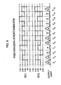
- FIG. 6A is a schematic diagram showing a general method of using the MZ modulator
- FIG. 6B is an explanatory diagram showing waveforms in the case where light is not extinguished
- FIG. 6C is an explanatory diagram showing waveforms in the case where light is extinguished.
- a RZ-modulated optical signal is inputted into the MZ modulator 103 from the left of the drawing.
- inputted are optical pulses equivalent to six bits (passing through the modulator 103 at times T1 to T6 respectively).
- the MZ modulator 103 receives as inputs two lines of RF signals RF1 and RF2, thereby performing modulation.
- a driving voltage of V ⁇ required to extinguish the input light can be reduced by half to a driving voltage of V ⁇ /2 by bringing the RF signals RF1 and RF2 in opposite phase.
- FIGS. 6B and 6C show the mechanism of extinction by a Mach-Zehnder (MZ) interferometer.
- MZ Mach-Zehnder
- the MZ interferometer at the input end, an input stream of light pulses is split into two pulse streams traveling through two arms, respectively. When traveling through the two arms, each pair of light pulses of the two pulse streams are shifted in phase and then combined at the output end. The amplitude of the combined light pulse is determined depending on the relative phase shift amount between two corresponding phase-shifted light pulses. For a bit not to extinguish, phase shifting is performed in the arms so that the resulting relative phase shift amount becomes 2N ⁇ (N is an integer).
- the phase of the light in one of the arms is shifted to (+ ⁇ /2 + 2N ⁇ ), and the phase of the light in the other arm is shifted to (- ⁇ /2 + 2M ⁇ ) (M is an integer), whereby the two streams of light after passing through the respective arms have a relative phase difference of ( ⁇ + 2(N + M) ⁇ ). Since two waves thus having a phase difference of ( ⁇ + (an integral multiple of 2 ⁇ )) cancel out each other when they are combined, the output of the MZ interferometer is extinguished.
- the relative biases of the RF signals RF1 and RF2 are controlled so that no extinction takes place at the times T2 and T5 and extinction takes place at the other times T1, T3, T4, and T6. Accordingly, the input light is transmitted to produce output light only at the times T2 and T5.
- the intensity ratio in intensity modulation can be set by determining the value of ⁇ .
- FIG. 7A is a waveform diagram for describing the intensity modulation operation of the MZ modulator
- FIG. 7B is a waveform diagram for describing the phase modulation operation of the MZ modulator
- FIG. 8 is a waveform diagram for describing the intensity and phase modulation operation of the MZ modulator.
- the waveforms of the output light show as examples the states of a modulated optical signal when the amplitudes of the signals RF1 and RF2 and the value of the offset, ⁇ V, are varied.
- the application voltage of the signal RF1 is 7.5 V (3V ⁇ /2) and the application voltage of the signal RF2 is 2.5 V (+V ⁇ /2). Therefore, the phase difference is ⁇ , resulting in the intensity of output light being lowered. However, this residual light that is not completely extinguished has an output phase of ⁇ . This is because the modulation voltages applied to the two arms can be considered to be ⁇ 2.5 V (V ⁇ /2) respectively with the center voltage at +5.0 V (V ⁇ ).
- the average of the voltages of the modulation signals applied to the two arms designates a modulation phase
- the relative difference between the voltages of the modulation signals designates a modulation intensity
- the MZ modulator 103 is driven with two multilevel signals, and the voltage difference between the two signals,
- the intensity-modulation signal and phase-modulation signal are "1" and "0", respectively, that is (1, 0)
- the same output as the bit at the time T1 can be obtained; when (0, 1), the same output as the bit at the time T4 can be obtained; and when (1, 1), the same output as the bit at the time T2 can be obtained.
- the MZ modulators 102 and 103 two modulators are used in the present mode: the MZ modulators 102 and 103.
- the fact that a small number of modulators are used makes a difference in the performance of a transmission system because of the optical loss in the modulators, not to mention the costs.
- catalog values for the insertion loss of a general LN modulator are approximately 5 dB, there is a difference of approximately 10 dB in loss in comparison with, for example, the scheme using four modulators as described in Hayase et al.
- the transmittable distance still decreases because a noise caused by the optical amplifier degrades the optical SNR.
- the present mode can also be applied to the case of using a non-return-to zero (NRZ) signal and to other multilevel coding that uses a larger number of levels.
- NRZ non-return-to zero
- D/A converters are used in the present mode to generate the electrical multilevel signals RF1 and RF2, analog operational device and the like may also be used as alternative means to generate electrical multilevel signals.
- the DC bias ( ⁇ V) to be applied at the final stage does not need to be V ⁇ /3 (V) but may be set depending on a desired set value of optical intensity.
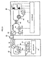
- FIG. 9 is a block diagram showing a configuration of a two-way quantum key distribution (QKD) system according to a first embodiment of the present invention.
- QKD quantum key distribution
- an optical pulse outputted from a laser light source 501 in the receiver 50 is sent to an optical coupler 503 by a circulator 502 and split into two pulses by the optical coupler 503.
- One of the two optical pulses is directly sent to a polarization beam splitter 505, allowed to pass through it, and then sent out to the transmission line 60.
- the other optical pulse is allowed through a phase modulator 504, sent to the polarization beam splitter 505, reflected there, and then sent out to the transmission line 60.
- the two optical pulses can be made to arrive at the polarization beam splitter 505 at different times by giving a difference between these two paths (short path and long path).
- the polarization beam splitter 505 combines the two sent optical pulses and sends them out to the transmission line 60, the two pulses are multiplexed in a state of being relatively time-divided, and sent as a double pulse to the sender 40 through the transmission line 60.
- the sender 40 After passing along the transmission line 60, the double pulse enters the sender 40.
- the sender 40 is provided with an optical attenuator 401, a polarization beam splitter 402, a MZ modulator 403, a MZ modulator driver 404, and a controller 405.
- the provision of the optical attenuator 401 depends on need and is not always necessary.
- the polarization beam splitter 402 and MZ modulator 403 constitute a polarization beam splitter (PBS) loop, which is a loop-back means for exhibiting to an optical pulse characteristics equivalent to the reflection characteristics of a Faraday mirror.
- PBS polarization beam splitter
- the MZ modulator driver 404 generates driving signals RF1 and RF2 by using four random numbers Rnd1 to Rnd4 supplied from the controller 405 and applies them to the MZ modulator 403. In addition, the controller 405 outputs an offset signal ⁇ V to the MZ modulator driver 404.
- Each pulse of the double pulse received from the receiver 50 is split by the polarization beam splitter 402 in accordance with the polarization state and is subjected to intensity modulation and phase modulation at the MZ modulator 403 while going round the PBS loop.
- the pulses going round the PBS loop are combined again by the polarization beam splitter 402 and sent out to the receiver 50 through the transmission line 60, as a returning double pulse.
- the polarizations of the optical pulses are rotated by 90 degrees each, by their going round the PBS loop, and in these respective polarization states, the optical pulses are sent out to the transmission line 60.
- the polarization beam splitter 505 outputs each of the optical pulses to one of the paths that is different from the path on the outward journey. Consequently, the two optical pulses, obtained by one optical pulse being split by the optical coupler 503 when sent out to the sender 40, both travel along the same-length paths, during which the double pulse is sent out from the receiver 50, reflected at the sender 40, and returned again to the receiver 50. The optical pulses are then combined again by the optical coupler 503, whereby interference occurs. The optical pulse in a single-photon state after the interference is detected by using balanced gated-mode photon detectors APD0 and APD1.
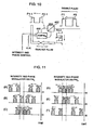
- FIG. 10 is a schematic diagram for describing the operation of the PBS loop in the sender 40.
- the pulses P1 and P2 of a double pulse received from the receiver 50 are each split into orthogonal polarization components by the polarization beam splitter 402, resulting in four pulses (quartet pulses) P1-1, P1-2, P2-1, and P2-2.
- the optical pulses P1-1 and P1-2 correspond to one polarization component and its orthogonal polarization component of the optical pulse P1, respectively
- the optical pulses P2-1 and P2-2 correspond to one polarization component and its orthogonal polarization component of the optical pulse P2, respectively.
- Two loop-side ports of the polarization beam splitter 402 are respectively connected to two optical ports of the MZ modulator 403 through polarization-maintaining optical fiber.
- the respective optical lines between the ports have different lengths.
- the lengths of the optical lines are set so that the optical pulses P1-1 and P2-1 enter the MZ modulator 403 earlier than the optical pulses P1-2 and P2-2, respectively, by a time difference T each.
- This time difference T is set longer than the width of an optical pulse and shorter than the interval between the pulses P1 and P2 of the double pulse.
- FIG. 11 is an explanatory diagram showing the temporal order of the optical pulses propagating through the MZ modulator. Since the optical pulses P1-1 and P2-1 arrive at the MZ modulator 403 earlier than the optical pulses P1-2 and P2-2, respectively, by the time difference T each, the optical pulses pass through the MZ modulator 403 at different times t2, t3, t4, and t5 as shown in FIGS. 11(B) to 11(E) . Therefore, the driving signals RF1 and RF2 to be applied to the MZ modulator 403 are changed in value in synchronization with the intervals between the pulses, whereby varying intensity differences and/or phase differences can be given between the pulses.
- FIG. 12A is a block diagram for describing the operation of the driver 404 for generating the driving signals RF1 and RF2 for driving the MZ modulator 403, and FIG. 12B is a table of correspondences for the levels of the driving signals RF1 and RF2.
- FIG. 13 is a waveform diagram conceptually showing signal conversion from random-number inputs (Rnd1, Rnd2, Rnd3, Rnd4) to the output signals RF1 and RF2.
- the driver 404 has functions of data conversion, clock multiplication, and amplification and generates two signals RF1 and RF2 (4f 0 b/s) from four random-number inputs Rnd1, Rnd2, Rnd3, and Rnd4 (f 0 b/s) and a clock signal CLK (f 0 Hz).
- each of the two output signals RF1 and RF2 is a signal having six levels of intensity, and the frequency of the output signals is four times higher than that of the input signals. Therefore, for a one-bit input, four bits are outputted each in a 1/4 time range (T1, T2, T3, T4), and the time ranges T1, T2, T3, and T4 correspond to FIGS. 11(B) to 11(E) , respectively.
- the voltage difference between each adjacent level of the six-level intensity signal is V ⁇ /2.
- the two-way QKD system uses the most typical QKD algorithm called BB84 protocol.
- the sender (Alice) 40 is provided with four random number sources.
- a random number Rnd1 supplies "0" or "1" for cryptographic key data, and a random number Rnd2 determines the way of data coding.
- a random number Rnd2 selects one of two coding sets (bases): one coding set of a 0-phase representing cryptographic key data "0" and a ⁇ -phase representing cryptographic key data "1" (hereinafter, this coding set will be referred to as “+ basis”), and the other coding set of a ⁇ /2-phase representing cryptographic key data "0” and a 3 ⁇ /2-phase representing cryptographic key data "1” (hereinafter, this coding set will be referred to as " ⁇ basis”). That is, any one of four types of modulation (0, ⁇ /2, ⁇ , 3 ⁇ /2) is randomly performed on an optical pulse.
- random numbers Rnd3 and Rnd4 are used as the random numbers for decoy intensity modulation. Referring to the table of level correspondences of FIG. 12B , it can be seen that when a random number Rnd4 is "1", the signals RF1 and RF2 are determined only by the values of random numbers Rnd1 and Rnd2, irrespective of the value of a random number Rnd3.
- the signals RF1 and RF2 are the same signals when a random number Rnd4 is "1"
- the optical pulses passing through the MZ modulator 403 are only subjected to phase modulation.
- multilevel-modulated optical outputs having three values for intensity and four values for phase can be obtained as shown in FIG. 13(d) .
- the thus multilevel-modulated double pulse is sent to the receiver (Bob) 50 through the transmission line 60.
- the receiver (Bob) 50 has a random number source for random numbers Rnd5 that correspond to the bases.
- the controller 506 drives the phase modulator 504 with a random number Rnd5 so that an optical pulse sent from the sender (Alice) 40 is decoded.
- a random number Rnd5 is "0”
- 0-phase (+ basis) modulation is performed on an optical pulse.
- ⁇ /2-phase (x basis) modulation is performed on an optical pulse.
- the receiver (Bob) 50 randomly obtains a value of "0" or "1", as a random number Rnd6, irrespective of the value of the corresponding random number Rnd1. Since each of the random numbers Rnd1, Rnd2, and Rnd5 varies with each one bit, the probability that the bases match and the probability that the bases do not match are both 50%.
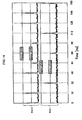
- FIG. 14 is a graph showing output results of a receiver-side interferometer in the case where optical intensity modulation with two values was additionally performed in quantum key distribution utilizing phase modulation.
- an experimental system as shown in FIG. 9 was used, and modulation using two values for phase and two values for intensity was performed in the sender (Alice) 40.
- the two ports for the outputs of the interferometer are denoted by Port0 (on the APD0 side) and Port1 (on the APD1 side).
- the graph of FIG. 14 shows the results when the optical pulse repetition rate is 62.5 Hz. From this graph, it can be seen that the output optical intensity was greatly reduced at times 64, 80, and 96 (ns) in comparison with the intensity at the other times. This level of intensity at the times 64, 80, and 96 is decoy level. Accordingly, it can be confirmed that it is possible to modulate the phase and intensity of an optical pulse at the same time through the present scheme.
- variable optical attenuator is provided in addition to a phase modulator, it is necessary to vary the timings when a train of optical pulses passes through these two devices on the outward and return journeys. This necessity makes the timing design complicated, imposing a limit to the QKD system driving rate.
- intensity modulation as well as four-state phase modulation, can be realized by one MZ modulator. Accordingly, since the timing should be considered for only one device, the timing design is facilitated, and at the same time, the QKD system driving rate can also be greatly enhanced. In addition, since the number of devices in use is reduced, the optical loss is also reduced, and the configuration is also simplified.
- the present invention is not limited to this embodiment.
- the present invention can also be applied to a general plug and play scheme using a Faraday mirror as shown in FIG. 2 .
- the QKD algorithm is not limited to the BB84 protocol either.
- the present invention can also be applied to the E91 protocol, the B92 protocol, and a method of coding information on a differential phase shift.
- the number of multiple levels for optical intensity is not limited to three.
- Levels (values) of optical intensity to be set are not limited to those described in the present embodiment either.
- the present invention can not only be applied to two-way quantum key distribution systems but also to one-way systems.
- FIG. 15 is a block diagram showing a schematic configuration of a one-way QKD system according to a second embodiment of the present invention.
- the present embodiment is a one-way QKD system using the planar lightwave circuit (PLC) described in Nambu, Y., et al., "One-way Quantum Key Distribution System based on Planar Lightwave Circuits," quant-ph/0603041 , to which the present invention is applied.
- a sender or transmitter (Alice) 70 and a receiver (Bob) 80 are connected through optical fiber 90 and each have an interferometer for time-delayed pulses, structured by using an asymmetric Mach-Zehnder interferometer (AMZI) based on PLC technology.
- a sender or transmitter (Alice) 70 and a receiver (Bob) 80 are connected through optical fiber 90 and each have an interferometer for time-delayed pulses, structured by using an asymmetric Mach-Zehnder interferometer (AMZI)
- the sender 70 has a pulse light source 701, an asymmetric Mach-Zehnder interferometer 702 based on a planar lightwave circuit, a MZ modulator 703 capable of intensity modulation and phase modulation, and a variable optical attenuator 704 that is provided as needed, as well as a synchronization section, a driver for driving the MZ modulator 703, a controller, and the like (not shown).
- the receiver 80 has a phase modulator 801, and an asymmetric Mach-Zehnder interferometer 802 based on a planar lightwave circuit, as well as a synchronization section, photon detectors, a controller, and the like (not shown).
- An optical pulse outputted from the pulse light source 701 of the sender 70 is split into two time-divided optical pulses (double pulse) by the asymmetric Mach-Zehnder interferometer 702, subjected to intensity modulation and/or phase modulation as described already at the MZ modulator 703, and then sent out to the receiver 80 through the variable optical attenuator 704.
- the arriving first and second optical pulses of the double pulse are subjected to phase modulation at the phase modulator 801, and each is further split by the asymmetric Mach-Zehnder interferometer 802, where the following one of the separate first pulses and the preceding one of the separate second pulses interfere with each other.
- the result of this interference is detected by one of the photon detectors.
- any of the BB84, E91, B92, and other protocols can be used. This embodiment can also be applied to a method of coding information on a differential phase shift.
- the present invention can be applied to general optical communications systems using the amplitude phase shift keying (APSK) scheme.
- APSK amplitude phase shift keying
- the present invention can be utilized in the technologies for generating random numbers by the detection of single photons, which are typified by the quantum key distribution technology that performs cryptographic key distribution by superposing information on the quantum states of single photons.
Landscapes
- Physics & Mathematics (AREA)
- Engineering & Computer Science (AREA)
- Electromagnetism (AREA)
- Computer Networks & Wireless Communication (AREA)
- Signal Processing (AREA)
- Optics & Photonics (AREA)
- Theoretical Computer Science (AREA)
- Computer Security & Cryptography (AREA)
- Optical Modulation, Optical Deflection, Nonlinear Optics, Optical Demodulation, Optical Logic Elements (AREA)
- Optical Communication System (AREA)
Claims (33)
- Dispositif de communication optique (10) pour transmettre séquentiellement des impulsions optiques (P1, P2, DP) à un autre dispositif de communication optique (20), dans lequel les impulsions optiques sont modulées à la fois en phase et en intensité, caractérisé en ce qu'il comprend :un modulateur optique (11) ayant une structure d'interféromètre qui comprend une pluralité de guides d'ondes optiques et d'électrodes prévues chacune en correspondance avec les guides d'ondes, dans lequel le modulateur optique permet la modulation à la fois de la phase et de l'intensité de chaque impulsion optique simultanément conformément à des signaux de commande (RF1, RF2) appliqués chacun aux électrodes ; etun dispositif de commande (12) pour commander le modulateur optique (11) en générant les signaux de commande (RF1, RF2) à partir d'informations de modulation pour moduler séparément la phase et l'intensité de l'impulsion optique,dans lequel le modulateur optique (11) est adapté pour moduler l'intensité de chaque impulsion optique (P1, P2, DP), avec l'un d'une pluralité de niveaux d'intensité comprenant un niveau très faible.
- Dispositif de communication optique selon la revendication 1, dans lequel l'intensité de chaque impulsion optique est modifiée de manière aléatoire en fonction des informations de modulation modulant l'intensité de l'impulsion optique.
- Dispositif de communication optique selon la revendication 1 ou 2, dans lequel le dispositif de commande génère les signaux de commande conformément à des premières informations qui provoquent la modulation de la phase de chaque impulsion optique et à des deuxièmes informations qui provoquent la modulation de l'intensité de l'impulsion optique, dans lequel les premières informations sont des informations à valeurs multiples correspondant à une pluralité de phases et les deuxièmes informations sont des informations à valeurs multiples correspondant à une pluralité d'intensités.
- Dispositif de communication optique selon la revendication 1, dans lequel le dispositif de commande fixe un rapport d'intensité pour la modulation d'intensité en ajustant le décalage d'au moins l'un des signaux de commande.
- Dispositif de communication optique selon la revendication 1, comprenant en outre une section de bouclage (402) pour recevoir l'impulsion optique de l'autre dispositif de communication optique et la renvoyer à l'autre dispositif de communication, dans lequel le modulateur optique (403) est prévu à une position prédéterminée sur un trajet optique dans la section de bouclage.
- Dispositif de communication optique selon la revendication 5, dans lequel la section de bouclage comprend un miroir de Faraday.
- Dispositif de communication optique selon la revendication 5, dans lequel la section de bouclage comprend une boucle de diviseur de faisceau par polarisation dans laquelle est prévu le modulateur optique.
- Dispositif de communication optique selon la revendication 1, dans lequel le modulateur optique (11) est un modulateur Mach-Zehnder à double électrode, dans lequel le dispositif de commande (12) comprend :un premier convertisseur numérique-analogique (111) pour générer un premier signal de modulation à partir d'informations de modulation de phase binaires entrées en tant que MSB et d'informations de modulation d'intensité binaires inversées entrées en tant que LSB ;un deuxième convertisseur numérique-analogique (112) pour générer un deuxième signal de modulation à partir des informations de modulation de phase binaires entrées en tant que MSB et des informations de modulation d'intensité binaires entrées en tant que LSB ;un premier amplificateur (113) pour amplifier le premier signal de modulation ;un deuxième amplificateur (114) pour amplifier le deuxième signal de modulation ; etun additionneur (115) pour ajouter un signal de décalage prédéterminé (δV) à un signal de sortie du deuxième amplificateur,dans lequel un signal de sortie du premier amplificateur est appliqué en tant que premier signal de commande à une électrode du modulateur Mach-Zehnder à électrode double et un signal de sortie de l'additionneur est appliqué en tant que deuxième signal de commande à l'autre électrode du modulateur Mach-Zehnder à électrode double.
- Dispositif de communication optique selon la revendication 8, dans lequel les premier et deuxième amplificateurs amplifient les premier et deuxième signaux de modulation respectivement de sorte qu'une différence de tension entre des niveaux adjacents des signaux de sortie des premier et deuxième amplificateurs devienne égale à un niveau qui est égal à la moitié d'une tension de commande Vπ du modulateur Mach-Zehnder à électrode double.
- Dispositif de communication optique selon la revendication 8 ou 9, dans lequel le signal de décalage prédéterminé amène le signal de sortie du deuxième amplificateur à s'écarter de la moitié de la tension de commande Vπ d'une tension prédéterminée.
- Système de distribution de clé quantique pour partager une chaîne de nombres aléatoires entre un émetteur (40) et un récepteur (50) tout en modifiant un nombre moyen de photons transmis de l'émetteur au récepteur, caractérisé en ce que l'émetteur (40) comprend :un modulateur optique (403) ayant une structure d'interféromètre qui comprend une pluralité de guides d'ondes optiques et d'électrodes prévues chacune en correspondance avec les guides d'ondes, dans lequel le modulateur optique permet la modulation simultanée à la fois de la phase et du nombre moyen de photons de chaque impulsion optique conformément à des signaux de commande (RF1, RF2) appliqués chacun aux électrodes ; etun dispositif de commande (404) pour commander le modulateur optique en générant les signaux de commande à partir d'informations de modulation (Rnd1 à Rnd4) pour moduler séparément la phase et le nombre moyen de photons de l'impulsion optique,dans lequel le modulateur optique est adapté pour moduler le nombre moyen de photons de chaque impulsion optique, qui est l'un d'une pluralité de nombres moyens de photons comprenant un très petit nombre de photons pour un niveau très faible.
- Système de distribution de clé quantique selon la revendication 11, dans lequel les informations de modulation consistent en une chaîne de nombres aléatoires.
- Système de distribution de clé quantique selon la revendication 11 ou 12, dans lequel le dispositif de commande génère les signaux de commande conformément à des premières informations qui provoquent la modulation de la phase de chaque impulsion optique et à des deuxièmes informations qui provoquent la modulation du nombre moyen de photons de l'impulsion optique, dans lequel les premières informations sont des informations à valeurs multiples correspondant à une pluralité de phases et les deuxièmes informations sont des informations à valeurs multiples correspondant à une pluralité de nombres moyens de photons.
- Système de distribution de clé quantique selon la revendication 11, dans lequel le dispositif de commande fixe un rapport des nombres moyens de photons modulés en ajustant le décalage d'au moins l'un des signaux de commande.
- Système de distribution de clé quantique selon la revendication 11, dans lequel l'émetteur comprend en outre une section de bouclage (402) pour recevoir l'impulsion optique du récepteur et la renvoyer au récepteur, dans lequel le modulateur optique est prévu à une position prédéterminée sur un trajet optique dans la section de bouclage.
- Système de distribution de clé quantique selon la revendication 15, dans lequel la section de bouclage comprend un miroir de Faraday.
- Système de distribution de clé quantique selon la revendication 15, dans lequel la section de bouclage comprend une boucle de diviseur de faisceau par polarisation dans laquelle le modulateur optique est inséré.
- Système de distribution de clé quantique selon la revendication 11, dans lequel le modulateur optique est un modulateur Mach-Zehnder à électrode double.
- Procédé de communication optique dans un dispositif de communication optique, pour transmettre séquentiellement des impulsions optiques à un autre dispositif de communication optique, dans lequel les impulsions optiques sont modulées à la fois en phase et en intensité par un modulateur optique ayant une structure d'interféromètre qui comprend une pluralité de guides d'ondes optiques et d'électrodes prévues chacune en correspondance avec les guides d'ondes, caractérisé en ce qu'il consiste à :générer des signaux de commande à partir d'informations de modulation pour moduler séparément la phase et l'intensité de l'impulsion optique ; etappliquer les signaux de commande aux électrodes du modulateur optique de manière à moduler à la fois la phase et l'intensité de chaque impulsion optique simultanément,dans lequel les signaux de commande sont générés de sorte qu'une pluralité de niveaux d'intensité avec lesquels le modulateur optique module l'intensité de chaque impulsion optique comprenne un niveau très faible.
- Procédé de communication optique selon la revendication 19, dans lequel l'intensité de chaque impulsion optique est modifiée de manière aléatoire en fonction des informations de modulation modulant l'intensité de l'impulsion optique.
- Procédé de communication optique selon la revendication 19 ou 20, dans lequel les signaux de commande comprennent des premières informations qui provoquent la modulation de la phase de chaque impulsion optique et des deuxièmes informations qui provoquent la modulation de l'intensité de l'impulsion optique, dans lequel les premières informations sont des informations à valeurs multiples correspondant à une pluralité de phases et les deuxièmes informations sont des informations à valeurs multiples correspondant à une pluralité d'intensités.
- Procédé de communication optique selon la revendication 19, dans lequel un rapport d'intensité pour la modulation d'intensité est fixé en ajustant le décalage d'au moins l'un des signaux de commande.
- Procédé de communication optique selon la revendication 19, dans lequel l'impulsion optique reçue de l'autre dispositif de communication optique est renvoyée à l'autre dispositif de communication, dans lequel le modulateur optique est prévu à une position prédéterminée sur un trajet optique de bouclage.
- Procédé de communication optique selon la revendication 23, dans lequel l'impulsion optique est renvoyée par un miroir de Faraday.
- Procédé de communication optique selon la revendication 23, dans lequel l'impulsion optique est renvoyée par une boucle de diviseur de faisceau par polarisation dans laquelle le modulateur optique est prévu.
- Procédé de communication optique selon la revendication 19, dans lequel le modulateur optique est un modulateur Mach-Zehnder à électrode double, dans lequel les signaux de commande sont générés en :générant un premier signal de modulation à partir d'informations de modulation de phase binaires entrées en tant que MSB et d'informations de modulation d'intensité binaires inversées entrées en tant que LSB ;générant un deuxième signal de modulation à partir des informations de modulation de phase binaires entrées en tant que MSB et des informations de modulation d'intensité binaires entrées en tant que LSB ;amplifiant le premier signal de modulation et le deuxième signal de modulation ; etajoutant un signal de décalage prédéterminé à un signal de sortie du deuxième amplificateur,dans lequel un signal amplifié du premier signal de modulation est appliqué en tant que premier signal de commande à une électrode du modulateur Mach-Zehnder à électrode double et un signal de somme obtenu par l'addition est appliqué en tant que deuxième signal de commande à l'autre électrode du modulateur Mach-Zehnder à électrode double.
- Procédé de communication optique selon la revendication 26, dans lequel les premier et deuxième signaux de modulation sont amplifiés de sorte qu'une différence de tension entre des niveaux adjacents de signaux amplifiés obtenus en amplifiant les premier et deuxième signaux de modulation devienne égale à un niveau qui est égal à la moitié d'une tension de commande Vπ du modulateur Mach-Zehnder à électrode double.
- Procédé de communication optique selon la revendication 26 ou 27, dans lequel le signal de décalage prédéterminé amène le signal amplifié obtenu en amplifiant le deuxième signal de modulation à s'écarter de la moitié de la tension de commande Vπ d'une tension prédéterminée.
- Procédé de distribution de clé quantique pour partager une chaîne de nombres aléatoires entre un émetteur et un récepteur tout en modifiant un nombre moyen de photons transmis de l'émetteur au récepteur, dans lequel l'émetteur comprend un modulateur optique ayant une structure d'interféromètre qui comprend une pluralité de guides d'ondes optiques et d'électrodes prévues chacune en correspondance avec les guides d'ondes, caractérisé en ce qu'il consiste à :générer des signaux de commande à partir d'informations de modulation pour moduler séparément la phase et le nombre moyen de photons de l'impulsion optique ; etappliquer les signaux de commande aux électrodes du modulateur optique de manière à moduler à la fois la phase et le nombre moyen de photons de chaque impulsion optique simultanément,dans lequel les signaux de commande sont générés de sorte que le nombre moyen de photons de chaque impulsion optique soit l'un d'une pluralité de nombres moyens de photons comprenant un très petit nombre de photons pour un niveau très faible.
- Procédé de distribution de clé quantique selon la revendication 29, dans lequel les informations de modulation sont une chaîne de nombres aléatoires.
- Procédé de distribution de clé quantique selon la revendication 29, dans lequel les signaux de commande sont générés conformément à une chaîne de premiers nombres aléatoires qui provoque la modulation de la phase de chaque impulsion optique et à une chaîne de deuxièmes nombres aléatoires qui provoque la modulation du nombre moyen de photons de l'impulsion optique, dans lequel la chaîne des premiers nombres aléatoires correspond à une pluralité de phases et la chaîne des deuxièmes nombres aléatoires correspond à une pluralité de nombres moyens de photons.
- Procédé de distribution de clé quantique selon la revendication 29, dans lequel un rapport des nombres moyens modulés de photons est fixé en ajustant le décalage d'au moins l'un des signaux de commande.
- Produit-programme d'ordinateur pour ordonner à un ordinateur de mettre en oeuvre un procédé de communication optique dans un dispositif de communication optique selon la revendication 1 ou 11, pour transmettre séquentiellement des impulsions optiques à un autre dispositif de communication optique, dans lequel les impulsions optiques sont modulées à la fois en phase et en intensité par un modulateur optique ayant une structure d'interféromètre qui comprend une pluralité de guides d'ondes optiques et d'électrodes prévues chacune en correspondance avec les guides d'ondes, caractérisé en ce qu'il consiste à :générer des signaux de commande à partir d'informations de modulation pour moduler séparément la phase et l'intensité de l'impulsion optique ; etappliquer les signaux de commande aux électrodes du modulateur optique de manière à moduler à la fois la phase et l'intensité de chaque impulsion optique simultanément,dans lequel les signaux de commande sont générés de sorte qu'une pluralité de niveaux d'intensité avec lesquels le modulateur optique module l'intensité de chaque impulsion optique comprenne un niveau très faible.
Applications Claiming Priority (1)
| Application Number | Priority Date | Filing Date | Title |
|---|---|---|---|
| JP2006116713A JP5196093B2 (ja) | 2006-04-20 | 2006-04-20 | 光通信装置およびそれを用いた量子暗号鍵配布システム |
Publications (2)
| Publication Number | Publication Date |
|---|---|
| EP1848128A1 EP1848128A1 (fr) | 2007-10-24 |
| EP1848128B1 true EP1848128B1 (fr) | 2010-10-27 |
Family
ID=38230174
Family Applications (1)
| Application Number | Title | Priority Date | Filing Date |
|---|---|---|---|
| EP07090078A Not-in-force EP1848128B1 (fr) | 2006-04-20 | 2007-04-20 | Dispositif de communication optique et système de distribution clé l'utilisant |
Country Status (4)
| Country | Link |
|---|---|
| US (1) | US7907850B2 (fr) |
| EP (1) | EP1848128B1 (fr) |
| JP (1) | JP5196093B2 (fr) |
| DE (1) | DE602007010049D1 (fr) |
Families Citing this family (40)
| Publication number | Priority date | Publication date | Assignee | Title |
|---|---|---|---|---|
| EP1730876A4 (fr) * | 2004-03-02 | 2008-04-02 | Magiq Technologies Inc | Synchronisation de modulateurs pour la distribution de cles quantiques |
| JP2007248850A (ja) * | 2006-03-16 | 2007-09-27 | Oki Electric Ind Co Ltd | マッハツェンダ型半導体素子及びその制御方法 |
| JP4893961B2 (ja) * | 2007-09-04 | 2012-03-07 | 日本電気株式会社 | 光送信器および複合変調器の制御方法 |
| JP5295624B2 (ja) * | 2008-04-28 | 2013-09-18 | 三菱電機株式会社 | 光送信器 |
| KR100983008B1 (ko) | 2008-05-30 | 2010-09-20 | 한국전자통신연구원 | 양자 암호 시스템 및 양자 암호 키의 분배 방법 |
| TWI382684B (zh) * | 2008-11-07 | 2013-01-11 | Univ Nat Chiao Tung | Dual Service Fiber Capture System |
| KR101253324B1 (ko) * | 2008-12-16 | 2013-04-12 | 한국전자통신연구원 | 양자화 암호 통신을 위한 광 숏 펄스 생성장치 및 방법 |
| JP5264521B2 (ja) | 2009-01-16 | 2013-08-14 | 三菱電機株式会社 | 光送信器 |
| US8588607B2 (en) * | 2009-01-29 | 2013-11-19 | Hewlett-Packard Development Company, L.P. | Dispersion scheme for physical layer diagnosis in bi-directional dual-fiber optical networks |
| JP2011022479A (ja) * | 2009-07-17 | 2011-02-03 | Mitsubishi Electric Corp | 多値光送信器 |
| KR101327661B1 (ko) * | 2009-12-21 | 2013-11-14 | 한국전자통신연구원 | 양자 암호키 분배를 위한 광위상 변조 방법 및 장치 |
| GB2476818B (en) * | 2010-01-08 | 2012-04-25 | Toshiba Res Europ Ltd | Quantum communication system and method |
| JP5682212B2 (ja) | 2010-10-06 | 2015-03-11 | ソニー株式会社 | 量子暗号通信装置と量子暗号通信方法および量子暗号通信システム |
| JP5957924B2 (ja) * | 2012-02-07 | 2016-07-27 | 日本電気株式会社 | 量子鍵配付装置および量子鍵配付方法 |
| JP5885297B2 (ja) * | 2012-02-15 | 2016-03-15 | Kddi株式会社 | 様々な変調形式の光信号を生成する装置および方法 |
| CA2882288C (fr) * | 2012-08-17 | 2020-10-27 | Los Alamos National Security, Llc | Systeme de communication quantique a dispositifs photoniques integres |
| ITMI20132014A1 (it) * | 2013-12-03 | 2015-06-04 | Milano Politecnico | Sistema di comunicazione ottica multilivello con una pluralità di sorgenti di radiazione ottica |
| JP6446803B2 (ja) * | 2014-03-25 | 2019-01-09 | 日本電気株式会社 | 光送受信器 |
| CN103986527B (zh) * | 2014-06-06 | 2016-08-17 | 中国科学技术大学 | 一种高速低电压相位调制方法 |
| US9313180B1 (en) * | 2015-03-31 | 2016-04-12 | Corning Incorporated | Systems and methods for quantum key generation |
| JP6550146B2 (ja) | 2015-03-31 | 2019-07-24 | コーニング インコーポレイテッド | 量子鍵生成のためのシステム及び方法 |
| CN106161402B (zh) * | 2015-04-22 | 2019-07-16 | 阿里巴巴集团控股有限公司 | 基于云环境的加密机密钥注入系统、方法及装置 |
| US9710230B2 (en) * | 2015-10-27 | 2017-07-18 | Fundació Insititut De Ciències Fotòniques | Process for quantum random number generation in a multimode laser cavity |
| EP3182638B1 (fr) * | 2015-12-18 | 2019-12-25 | ID Quantique S.A. | Appareil et procédé permettant d'ajouter une source d'entropie pour systèmes de distribution de clé quantique |
| GB2551685B (en) * | 2016-02-16 | 2019-12-11 | Toshiba Kk | An optical device, a transmitter for a quantum communication system and a quantum communication system |
| CN106230511B (zh) * | 2016-08-31 | 2018-07-17 | 南京恩瑞特实业有限公司 | 5g分布式基站天线射频光传输系统 |
| CN106712947B (zh) * | 2017-03-24 | 2023-08-18 | 浙江九州量子信息技术股份有限公司 | 一种基于量子密钥分配系统的驱动电路 |
| GB2571521B (en) * | 2018-02-22 | 2021-07-07 | Toshiba Kk | A transmitter for a quantum communication system, a quantum communication system and a method of generating intensity modulated Photon pulses |
| CN110351070B (zh) * | 2018-04-02 | 2024-06-21 | 浙江九州量子信息技术股份有限公司 | 一种基于y波导的量子密钥分发系统及方法 |
| CN108540282A (zh) * | 2018-05-02 | 2018-09-14 | 如般量子科技有限公司 | 基于偏振调制时间编码的hd-qkd系统 |
| CN108650088B (zh) * | 2018-07-04 | 2023-10-20 | 中国科学技术大学 | 包含至少三方的量子通信装置及方法 |
| CN109039618B (zh) * | 2018-10-29 | 2023-08-04 | 中国电子科技集团公司电子科学研究院 | 量子密钥分发相位解码方法和装置及相应系统 |
| CN109039619B (zh) * | 2018-10-29 | 2023-05-26 | 中国电子科技集团公司电子科学研究院 | 量子密钥分发时间比特-相位解码方法和装置及相应系统 |
| CN109343173B (zh) * | 2018-12-06 | 2023-08-25 | 安徽问天量子科技股份有限公司 | 一种混合波导集成的干涉仪 |
| JP7561776B2 (ja) * | 2019-06-17 | 2024-10-04 | ケーティー コーポレーション | 量子暗号キー分配方法、装置及びシステム |
| WO2021250829A1 (fr) * | 2020-06-10 | 2021-12-16 | 日本電気株式会社 | Émetteur optique et procédé de détermination d'exactitude/d'inexactitude de synchronisation de modulation |
| CN114696212B (zh) * | 2020-12-29 | 2025-10-31 | 科大国盾量子技术股份有限公司 | 光强实时维稳装置及方法、量子密钥分发系统及其发射端 |
| US12212669B2 (en) * | 2021-02-19 | 2025-01-28 | Eagle Technology, Llc | Quantum communications system using pulse divider and associated methods |
| CN113364526B (zh) * | 2021-05-21 | 2022-07-26 | 电子科技大学 | 一种微波多相位差分相移键控信号的光学解调系统 |
| CN114401089B (zh) * | 2022-01-26 | 2024-04-26 | 杭州慧明量子通信技术有限公司 | 一种可调延时干涉仪及量子密钥分发系统 |
Family Cites Families (11)
| Publication number | Priority date | Publication date | Assignee | Title |
|---|---|---|---|---|
| US5515438A (en) * | 1993-11-24 | 1996-05-07 | International Business Machines Corporation | Quantum key distribution using non-orthogonal macroscopic signals |
| US5953421A (en) * | 1995-08-16 | 1999-09-14 | British Telecommunications Public Limited Company | Quantum cryptography |
| DK0923828T3 (da) * | 1996-09-05 | 2004-05-24 | Swisscom Ag | Kvantekryptografiindretning og fremgangsmåde |
| JPH1152313A (ja) * | 1997-08-08 | 1999-02-26 | Mitsubishi Electric Corp | 光変調装置 |
| US6188768B1 (en) * | 1998-03-31 | 2001-02-13 | International Business Machines Corporation | Autocompensating quantum cryptographic key distribution system based on polarization splitting of light |
| US7023601B2 (en) * | 2002-12-02 | 2006-04-04 | Nortel Networks Limited | Optical E-field modulation using a Mach-Zehnder interferometer |
| JP5142095B2 (ja) * | 2003-11-28 | 2013-02-13 | 独立行政法人科学技術振興機構 | 通信システム及びそれを用いた通信方法 |
| US7181011B2 (en) * | 2004-05-24 | 2007-02-20 | Magiq Technologies, Inc. | Key bank systems and methods for QKD |
| US7321734B2 (en) * | 2004-07-29 | 2008-01-22 | Nortel Networks Limited | Digital synthesis of readily compensated optical signals |
| JP4784202B2 (ja) | 2004-09-02 | 2011-10-05 | 日本電気株式会社 | 多重化通信システムおよびそのクロストーク除去方法 |
| US7277603B1 (en) * | 2006-02-22 | 2007-10-02 | Nortel Networks Limited | Integrated optical waveform modulation |
-
2006
- 2006-04-20 JP JP2006116713A patent/JP5196093B2/ja not_active Expired - Fee Related
-
2007
- 2007-04-20 EP EP07090078A patent/EP1848128B1/fr not_active Not-in-force
- 2007-04-20 US US11/788,707 patent/US7907850B2/en not_active Expired - Fee Related
- 2007-04-20 DE DE602007010049T patent/DE602007010049D1/de active Active
Also Published As
| Publication number | Publication date |
|---|---|
| US20070248362A1 (en) | 2007-10-25 |
| JP5196093B2 (ja) | 2013-05-15 |
| EP1848128A1 (fr) | 2007-10-24 |
| DE602007010049D1 (de) | 2010-12-09 |
| JP2007286551A (ja) | 2007-11-01 |
| US7907850B2 (en) | 2011-03-15 |
Similar Documents
| Publication | Publication Date | Title |
|---|---|---|
| EP1848128B1 (fr) | Dispositif de communication optique et système de distribution clé l'utilisant | |
| US8041232B2 (en) | Optical transmitter and control method thereof | |
| Kahn et al. | Spectral efficiency limits and modulation/detection techniques for DWDM systems | |
| US7613396B2 (en) | Multiplexing communication system and crosstalk elimination method | |
| EP0923828B1 (fr) | Dispositif et procede de cryptographie quantique | |
| Eriksson et al. | Coexistence of continuous variable quantum key distribution and 7× 12.5 Gbit/s classical channels | |
| Dong-Nhat et al. | Investigations of high-speed optical transmission systems employing absolute added correlative coding (AACC) | |
| CN101170363B (zh) | 一种光差分偏振位移键控系统及其信号发送装置与方法 | |
| JP2006203886A (ja) | オフセット直交位相偏移変調方法とこれを用いる光送信器 | |
| JP5347644B2 (ja) | 光通信システム及び方法、送信機及び受信機、量子暗号鍵配付システム及び方法 | |
| Kikuchi et al. | Incoherent 32-level optical multilevel signaling technologies | |
| Eriksson et al. | Biorthogonal modulation in 8 dimensions experimentally implemented as 2PPM-PS-QPSK | |
| Khalil et al. | Security performance of public key distribution in coherent optical communications links | |
| US20250254033A1 (en) | Quantum communication system that switches between quantum key distribution (qkd) protocols and associated methods | |
| Honjo et al. | Quantum key distribution experiment through a PLC matrix switch | |
| KR102576065B1 (ko) | 직교 위상 성분 값의 제어된 분포를 갖는 광학 펄스의 생성 | |
| Nakazawa et al. | Real-time 70 gbit/s, 128 QAM quantum noise stream cipher transmission over 100 km with secret keys delivered by continuous variable quantum key | |
| Li et al. | Demonstration of Polarization-insensitive Coherent 56Gb/s/λ PAM-4 PON using Real-valued Alamouti Coding Combined with Digital Pilot | |
| JP5413687B2 (ja) | 光通信システム、光通信方法および光通信装置 | |
| JP7776121B2 (ja) | 送信器および多値伝送方法 | |
| Djordjevic | Hybrid DV-CV QKD outperforming existing QKD protocols in terms of secret-key rate and achievable distance | |
| Bogdanski et al. | Multiuser quantum key distribution over telecom fiber networks | |
| Wen et al. | Simultaneous all-optical transparent phase multiplexing/de-multiplexing based on FWM in a HNLF | |
| Kikuchi | Amplitude and phase modulated 8-ary and 16-ary multilevel signaling technologies for high-speed optical fiber communication | |
| Chi et al. | Improved label property of orthogonal ASK/DPSK labeling by using a 40 Gb/s Manchester coded payload |
Legal Events
| Date | Code | Title | Description |
|---|---|---|---|
| PUAI | Public reference made under article 153(3) epc to a published international application that has entered the european phase |
Free format text: ORIGINAL CODE: 0009012 |
|
| AK | Designated contracting states |
Kind code of ref document: A1 Designated state(s): AT BE BG CH CY CZ DE DK EE ES FI FR GB GR HU IE IS IT LI LT LU LV MC MT NL PL PT RO SE SI SK TR |
|
| AX | Request for extension of the european patent |
Extension state: AL BA HR MK YU |
|
| 17P | Request for examination filed |
Effective date: 20080318 |
|
| AKX | Designation fees paid |
Designated state(s): CH DE FR GB LI |
|
| GRAP | Despatch of communication of intention to grant a patent |
Free format text: ORIGINAL CODE: EPIDOSNIGR1 |
|
| GRAS | Grant fee paid |
Free format text: ORIGINAL CODE: EPIDOSNIGR3 |
|
| GRAA | (expected) grant |
Free format text: ORIGINAL CODE: 0009210 |
|
| AK | Designated contracting states |
Kind code of ref document: B1 Designated state(s): CH DE FR GB LI |
|
| REG | Reference to a national code |
Ref country code: GB Ref legal event code: FG4D |
|
| REG | Reference to a national code |
Ref country code: CH Ref legal event code: EP Ref country code: CH Ref legal event code: NV Representative=s name: E. BLUM & CO. AG PATENT- UND MARKENANWAELTE VSP |
|
| REF | Corresponds to: |
Ref document number: 602007010049 Country of ref document: DE Date of ref document: 20101209 Kind code of ref document: P |
|
| PLBE | No opposition filed within time limit |
Free format text: ORIGINAL CODE: 0009261 |
|
| STAA | Information on the status of an ep patent application or granted ep patent |
Free format text: STATUS: NO OPPOSITION FILED WITHIN TIME LIMIT |
|
| 26N | No opposition filed |
Effective date: 20110728 |
|
| REG | Reference to a national code |
Ref country code: DE Ref legal event code: R097 Ref document number: 602007010049 Country of ref document: DE Effective date: 20110728 |
|
| GBPC | Gb: european patent ceased through non-payment of renewal fee |
Effective date: 20110420 |
|
| PG25 | Lapsed in a contracting state [announced via postgrant information from national office to epo] |
Ref country code: DE Free format text: LAPSE BECAUSE OF NON-PAYMENT OF DUE FEES Effective date: 20111101 |
|
| PG25 | Lapsed in a contracting state [announced via postgrant information from national office to epo] |
Ref country code: GB Free format text: LAPSE BECAUSE OF NON-PAYMENT OF DUE FEES Effective date: 20110420 |
|
| REG | Reference to a national code |
Ref country code: DE Ref legal event code: R119 Ref document number: 602007010049 Country of ref document: DE Effective date: 20111101 |
|
| REG | Reference to a national code |
Ref country code: FR Ref legal event code: PLFP Year of fee payment: 10 |
|
| REG | Reference to a national code |
Ref country code: FR Ref legal event code: PLFP Year of fee payment: 11 |
|
| REG | Reference to a national code |
Ref country code: FR Ref legal event code: PLFP Year of fee payment: 12 |
|
| PGFP | Annual fee paid to national office [announced via postgrant information from national office to epo] |
Ref country code: FR Payment date: 20220421 Year of fee payment: 16 |
|
| PGFP | Annual fee paid to national office [announced via postgrant information from national office to epo] |
Ref country code: CH Payment date: 20220421 Year of fee payment: 16 |
|
| REG | Reference to a national code |
Ref country code: CH Ref legal event code: PL |
|
| PG25 | Lapsed in a contracting state [announced via postgrant information from national office to epo] |
Ref country code: LI Free format text: LAPSE BECAUSE OF NON-PAYMENT OF DUE FEES Effective date: 20230430 Ref country code: FR Free format text: LAPSE BECAUSE OF NON-PAYMENT OF DUE FEES Effective date: 20230430 Ref country code: CH Free format text: LAPSE BECAUSE OF NON-PAYMENT OF DUE FEES Effective date: 20230430 |