EP1848254A2 - Module de panneau à circuit - Google Patents
Module de panneau à circuit Download PDFInfo
- Publication number
- EP1848254A2 EP1848254A2 EP07006010A EP07006010A EP1848254A2 EP 1848254 A2 EP1848254 A2 EP 1848254A2 EP 07006010 A EP07006010 A EP 07006010A EP 07006010 A EP07006010 A EP 07006010A EP 1848254 A2 EP1848254 A2 EP 1848254A2
- Authority
- EP
- European Patent Office
- Prior art keywords
- circuit board
- printed circuit
- board module
- module according
- modules
- Prior art date
- Legal status (The legal status is an assumption and is not a legal conclusion. Google has not performed a legal analysis and makes no representation as to the accuracy of the status listed.)
- Ceased
Links
Images



Classifications
-
- H—ELECTRICITY
- H05—ELECTRIC TECHNIQUES NOT OTHERWISE PROVIDED FOR
- H05K—PRINTED CIRCUITS; CASINGS OR CONSTRUCTIONAL DETAILS OF ELECTRIC APPARATUS; MANUFACTURE OF ASSEMBLAGES OF ELECTRICAL COMPONENTS
- H05K1/00—Printed circuits
- H05K1/02—Details
- H05K1/14—Structural association of two or more printed circuits
- H05K1/142—Arrangements of planar printed circuit boards in the same plane, e.g. auxiliary printed circuit insert mounted in a main printed circuit
-
- H—ELECTRICITY
- H05—ELECTRIC TECHNIQUES NOT OTHERWISE PROVIDED FOR
- H05K—PRINTED CIRCUITS; CASINGS OR CONSTRUCTIONAL DETAILS OF ELECTRIC APPARATUS; MANUFACTURE OF ASSEMBLAGES OF ELECTRICAL COMPONENTS
- H05K1/00—Printed circuits
- H05K1/02—Details
- H05K1/14—Structural association of two or more printed circuits
- H05K1/148—Arrangements of two or more hingeably connected rigid printed circuit boards, i.e. connected by flexible means
-
- F—MECHANICAL ENGINEERING; LIGHTING; HEATING; WEAPONS; BLASTING
- F21—LIGHTING
- F21K—NON-ELECTRIC LIGHT SOURCES USING LUMINESCENCE; LIGHT SOURCES USING ELECTROCHEMILUMINESCENCE; LIGHT SOURCES USING CHARGES OF COMBUSTIBLE MATERIAL; LIGHT SOURCES USING SEMICONDUCTOR DEVICES AS LIGHT-GENERATING ELEMENTS; LIGHT SOURCES NOT OTHERWISE PROVIDED FOR
- F21K9/00—Light sources using semiconductor devices as light-generating elements, e.g. using light-emitting diodes [LED] or lasers
-
- H—ELECTRICITY
- H05—ELECTRIC TECHNIQUES NOT OTHERWISE PROVIDED FOR
- H05K—PRINTED CIRCUITS; CASINGS OR CONSTRUCTIONAL DETAILS OF ELECTRIC APPARATUS; MANUFACTURE OF ASSEMBLAGES OF ELECTRICAL COMPONENTS
- H05K2201/00—Indexing scheme relating to printed circuits covered by H05K1/00
- H05K2201/09—Shape and layout
- H05K2201/09209—Shape and layout details of conductors
- H05K2201/09372—Pads and lands
- H05K2201/09481—Via in pad; Pad over filled via
-
- H—ELECTRICITY
- H05—ELECTRIC TECHNIQUES NOT OTHERWISE PROVIDED FOR
- H05K—PRINTED CIRCUITS; CASINGS OR CONSTRUCTIONAL DETAILS OF ELECTRIC APPARATUS; MANUFACTURE OF ASSEMBLAGES OF ELECTRICAL COMPONENTS
- H05K2201/00—Indexing scheme relating to printed circuits covered by H05K1/00
- H05K2201/09—Shape and layout
- H05K2201/09209—Shape and layout details of conductors
- H05K2201/095—Conductive through-holes or vias
- H05K2201/096—Vertically aligned vias, holes or stacked vias
-
- H—ELECTRICITY
- H05—ELECTRIC TECHNIQUES NOT OTHERWISE PROVIDED FOR
- H05K—PRINTED CIRCUITS; CASINGS OR CONSTRUCTIONAL DETAILS OF ELECTRIC APPARATUS; MANUFACTURE OF ASSEMBLAGES OF ELECTRICAL COMPONENTS
- H05K2201/00—Indexing scheme relating to printed circuits covered by H05K1/00
- H05K2201/09—Shape and layout
- H05K2201/09818—Shape or layout details not covered by a single group of H05K2201/09009 - H05K2201/09809
- H05K2201/09845—Stepped hole, via, edge, bump or conductor
-
- H—ELECTRICITY
- H05—ELECTRIC TECHNIQUES NOT OTHERWISE PROVIDED FOR
- H05K—PRINTED CIRCUITS; CASINGS OR CONSTRUCTIONAL DETAILS OF ELECTRIC APPARATUS; MANUFACTURE OF ASSEMBLAGES OF ELECTRICAL COMPONENTS
- H05K2201/00—Indexing scheme relating to printed circuits covered by H05K1/00
- H05K2201/10—Details of components or other objects attached to or integrated in a printed circuit board
- H05K2201/10007—Types of components
- H05K2201/10106—Light emitting diode [LED]
-
- H—ELECTRICITY
- H05—ELECTRIC TECHNIQUES NOT OTHERWISE PROVIDED FOR
- H05K—PRINTED CIRCUITS; CASINGS OR CONSTRUCTIONAL DETAILS OF ELECTRIC APPARATUS; MANUFACTURE OF ASSEMBLAGES OF ELECTRICAL COMPONENTS
- H05K2201/00—Indexing scheme relating to printed circuits covered by H05K1/00
- H05K2201/10—Details of components or other objects attached to or integrated in a printed circuit board
- H05K2201/10227—Other objects, e.g. metallic pieces
- H05K2201/10409—Screws
-
- H—ELECTRICITY
- H05—ELECTRIC TECHNIQUES NOT OTHERWISE PROVIDED FOR
- H05K—PRINTED CIRCUITS; CASINGS OR CONSTRUCTIONAL DETAILS OF ELECTRIC APPARATUS; MANUFACTURE OF ASSEMBLAGES OF ELECTRICAL COMPONENTS
- H05K3/00—Apparatus or processes for manufacturing printed circuits
- H05K3/30—Assembling printed circuits with electric components, e.g. with resistors
- H05K3/32—Assembling printed circuits with electric components, e.g. with resistors electrically connecting electric components or wires to printed circuits
- H05K3/325—Assembling printed circuits with electric components, e.g. with resistors electrically connecting electric components or wires to printed circuits by abutting or pinching; Mechanical auxiliary parts therefor
Definitions
- the invention relates to a printed circuit board module.
- PCB modules There are PCB modules known that are not installed in devices, but to take over certain functions outside of devices. For example, they can be printed circuit boards with lighting whose sole purpose is to make advertisements appear in certain places.
- the invention is based on the object to provide a way PCB modules with little effort universally with each other to be able to connect without the need for additional or special connection devices.
- the invention proposes a printed circuit board module with the features mentioned in claim 1. Further developments of the invention are the subject of dependent claims.
- a connecting device is formed on the printed circuit board module itself, which is designed and suitable for direct direct connection to another printed circuit board module having the same or similar connection device. This makes it possible to manage without intermediate elements between two printed circuit board modules, and it is also possible to build larger chains of printed circuit board modules of identical printed circuit board modules.
- a printed circuit board module can have a coupling device which can be connected to a plug or plug pins, for example.
- a module in which the coupling of the power supply takes place, can also be referred to as the end module, since it is arranged at the end or at the beginning of such a chain of printed circuit board modules. It is then, for example, only connect to a single additional circuit board.
- middle modules can be formed, which are characterized in that they have two connection devices for connection to two other modules. Again, the connecting devices are again formed directly on the module.
- modules should take over certain tasks.
- a module can be present which has no other task than mechanically and electrically connecting two other modules. So it has only continuous tracks, which are not connected with other things within this module.
- a module has at least one LED, which is connected to the strip conductors which pass through the module.
- a module it is also possible for a module to have an electronic component supplied with power by means of the conductor tracks, in order to form a functional module.
- a module has a logic component for forming a logic module.
- the circuit board module is strip-shaped, in which case in particular the shape of a flat strip is preferred, in which a broadside the front and a broad side forms the back of the printed circuit board module.
- the strip has a square or approximately square cross-section, to form a rod.
- the bar may be an angled bar, it may also have a branch, so that the PCB module has three or more than three connection points, of which optionally each connection point is provided with connection means for coupling to a similar module.
- the module can be designed, in particular, as a rectilinear strip. So here not only the front and the back lie in one plane, but also the top and bottom, which can also be called edges.
- the curvature is present in one dimension.
- the front and back sides are still in one plane while the top and bottom edges are curved.
- the printed circuit board module can be both a rigid printed circuit board and a rigidly flexible printed circuit board.
- the connecting device is designed such that two adjacent modules in different positions are connected to each other, the different positions differ in different angular positions about an axis perpendicular to the front or back of the PCB module in the area the connection runs.
- the connecting device can be such that the individual modules can be plugged together in these different positions.
- the connecting device may be formed in a development so that when manufactured connection, the front sides and backs of the two adjacent modules also lie in the area of the connection in the same plane.
- the connecting device like a hinge, that is with an axis forming a connecting element, around which then the two modules are pivotable.
- the connecting device may comprise contact elements which are formed such that the contact elements of the connecting device of one printed circuit board lie flat against the contact elements of the connecting device of the other printed circuit board module.
- the mechanical connecting element for example a screw, serve to produce a sufficient surface pressure.
- the contact element may be formed as slip rings, which ensure an electrical connection in any angular positions.
- a mechanical connecting element for example a connecting element forming the hinge axis, acts as a conductor.
- the connecting devices connect more than two conductor tracks to one another, so that a plurality of circuits may also be arranged in the circuit board modules can. This can for example be done so that slip rings are formed as concentric circles.
- the connecting device can be designed, for example, mechanically such that, starting from the front side of the printed circuit board module, a step is formed on the surface of which the sliding rings are arranged. Then, the adjacent circuit board module is connected in reverse order so that the front and back sides of the two adjacent modules are actually in the same plane.
- This sliding joint connection can in particular have a length compensation in order to be able to compensate for tolerances in the attachment.
- the printed circuit board module may have a multilayer construction in development of the invention.
- the printed circuit board module can have a socket, for example a socket.
- a socket for example a socket.
- This can serve to establish or carry out electrical and / or control connections.
- it can be a jack socket or even a USB interface, in which not only the mechanical shape is normalized, but also the electrical properties.
- Such a socket for example, a USB socket, can serve to plug in a power supply unit.
- FIGS 1 to 3 show in three different views a printed circuit board module according to a first embodiment of the invention.
- the printed circuit board module is formed as a flat elongated strip, with a rectilinear upper edge 1, a lower edge 2 extending parallel thereto, a flat front side 3 and a flat rear side 4.
- the front side 3 is stepped, so that a step 5 is formed, which is offset by about half the thickness of the printed circuit board module to the rear.
- a hole 6 is present in each case.
- the boundary line 7 of level 5 extends above a longitudinal center line along the same arc as the end itself.
- LEDs 8 are arranged in the example shown, which are in communication with existing in the printed circuit board conductor tracks. Since the edge 1 of the circuit board module is narrow, the LEDs 8 are arranged along a line.
- the front side 3 of the printed circuit board module is also provided with LEDs 8. These could also be arranged at different heights, as shown by the front side 3 of the printed circuit board of FIG.
- FIGS. 4 and 5 show a similar printed circuit board module having the same height, the same thickness and the same peripheral shape in the end region as the printed circuit board module of FIGS. 1 to 3.
- the comparison of the two embodiments shows that the printed circuit board module of the present invention can be made in any length.
- FIG. 6 shows, similar to FIG. 2, an edge view of a further module.
- the stage 5 is formed on the back 4 in the region of one end, while at the other end, the step 5 is formed on the front side 3 of the printed circuit board module. This allows the individual modules to string together without having to turn them over.
- LEDs 8 are arranged on all sides of the printed circuit board module.
- a printed circuit board module is rigid-flexible, which means that it has in its central region a flexible portion 10, which makes it possible to arrange the two arranged beyond the flexible portion parts in different levels.
- the flexible portion 10 which connects the two parts of the printed circuit board module together is formed in the region of the back 4 of the printed circuit board module.
- the two parts can be bent on both sides of the flexible portion 10 to the rear to form an outer corner. Due to the elasticity of the region 10, an arrangement is therefore possible in which both parts of the printed circuit board module do not lie in one plane.
- Figure 9 is intended to indicate how two modules are interconnected and which arrangements are possible.
- the left end of a printed circuit board module As shown in Figure 1, the left end of another printed circuit board module is arranged ready for connection.
- the right PCB modules is reversed so that now the back 4 can be seen and the level 5 on the other side not visible here.
- FIG. 9 shows the front view
- FIG. 10 shows a view from above.
- an end module 11 in which the left end can serve to couple in electricity. This can be done with the help of soldered cables or with a plug connection.
- the right end of this end module is formed as shown on the right in Figure 1 also.
- the end module is followed by a module in which the rear side 4 is directed forward, then again a reverse oriented module.
- FIG. 11 shows that a module can also have the shape of a bar having a branch, so that three branches each having a step 5 are formed at the end of each branch.
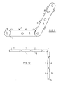
- Figure 12 shows a module which is also designed as a bar, but this time as an angled bar. In the example shown it is It is a right-angled bend, but this is also not necessary.
- FIGS. 11 and 12 show that it is possible to arrange the LEDs only on the front side or, in other words, the front side 3 ,
- For mechanical connection of the modules can serve screws that can be inserted through the holes 6 of the ends of the modules and then secured with nuts, for example.
- the provided in its center with the hole 6 stage 5 thus forms, together with a connecting element in the form of a screw, for example, a connecting device to mechanically connect two modules together.
- This connecting device is, with the exception of the screw as a connecting element, directly formed on the printed circuit board module itself.
- FIG. 13 shows a longitudinal section through the end region of a printed circuit board module.
- the center of the step 5 arranged bore 6 is formed as a plated through hole, which means that its wall is provided with a metallic sleeve 12.
- this sleeve 12 widens and forms a flat disc whose free surface lies in a plane.
- the through-hole in the form of the sleeve 12 is initially surrounded by a concentric ring, in which the material of the circuit board is not provided with a conductive coating. Outside of this thus insulating ring area a contact 13 is present, which merges directly into the conductor tracks 14. This contact 13 forms a slip ring.
- two separate conductor strands are connected to one another, namely firstly through the connection of the through-plated holes, and secondly through the contact between the slip rings 13.
- the mechanical connection of two or more printed circuit board modules 1 can be done by hollow rivets, blind rivets, screws or the like. Screws can additionally serve the connection point to screw on a base. By using electrically conductive materials, such as metal rivets and metal screws, an electrical connection can be made simultaneously.
- non-conductive materials may also be used, for example plastic blind rivets.
- a sleeve 16 is inserted into the bore 6, which projects on the opposite side, ie the stage 5, to the top of the tracks 14. He is surrounded by a slip ring 13 at a distance.
- a further connection device can cooperate, which has a larger diameter bore 6, which corresponds to the outer diameter of the sleeve 16.
- Figure 16 shows, in a fragmentary view, the ends of three printed circuit board modules, with the step 5 in the left printed circuit board module starting from the front side 3 and corresponding to about two thirds of the thickness of the printed circuit board, while the right lower printed circuit board module is just reversed.
- the right upper circuit board module has the opposite two stages 5, one of which emanates from the back 4 and the other from the front 3. If the lower right-hand printed circuit board module is folded upwards or downwards by 90 ° with respect to the plane of the drawing, three printed circuit board modules can be connected to one another in a star shape, in which case the front sides 3 and the back sides 4 are arranged flush in each case in one plane.
- FIG. 17 likewise shows in a very simplified manner a printed circuit board module which has an approximately square cross-section. At one end, the step 5 starts from the top 1, and at the other end from the front 3. As a result, joints can be formed with hinge axes that are perpendicular to each other and not parallel, as in the previous embodiments. Of course, other angles are conceivable than the right angle between the two hinge axes in the embodiment of Figure 17. This allows chains form of the PCB modules that leave a plane.
- a mechanical connection element such as a screw or a rivet, which is inserted through the mutually aligned holes 6 of the two connecting devices through and forms an axis for the hinge.
- Figure 18 shows the possibility of how two circuit board modules can be connected together so that they can be arranged only in mutual extension but allow for a certain length compensation.
- the printed circuit board module 1 shown on the left in FIG. 18 has a slot 16 in the region having the step 5.
- the corresponding end of the printed circuit board module shown on the right in FIG. 18 has on its downwardly directed step 5 a projection 17 whose width is equal to the width of the module Long hole 16 corresponds, but whose length is shorter than the length of the slot 16.
- the lug 17 is a hollow lug, then a screw can be inserted through it, such as with a washer on the bottom causes a distortion of the two circuit board modules 1.
- a screw can be inserted through it, such as with a washer on the bottom causes a distortion of the two circuit board modules 1.
- Figure 19 shows two ways in which the end portions of the circuit board modules having the holes 6 can be made different.
- the side edges of the printed circuit board module converge in the direction of an eyelet 18, while in the printed circuit board module on the right in FIG. 19, a connecting web 19 leads to the eyelet 18.
- This connecting web is formed with parallel side edges.
- the step 5 only needs to be present in the region of the eyelet 18 itself.
- FIG. 20 shows that such an eyelet 18 having the hole 6 can also be connected to the printed circuit board module 1 via an angled connecting web 19 or else via an obliquely extending connecting web 19.
- Figure 21 shows an end view of a printed circuit board module having a socket 20 which is formed as a USB socket.
- a USB plug or a USB stick can be plugged in. This can be used, for example, for energy supply if it contains a battery or a battery emulator.
- USB socket 20 can also be arranged at other locations of a printed circuit board, for example at the side edge.
- FIGS. 22 to 24 show ways in which two modules 1 can be connected to one another in a similar manner, as FIG. 18 shows.
- the one module shown in Figure 22, contains the step in that 5 having a T-shaped slot 26, wherein the web of the T is directed to the stage 15, while the broadening is present below the level 5.
- the counterpart which is shown in front view in Figure 23, below the step 5 via a web 27 connected to a transverse plate 28.
- the width of the transverse plate 28 corresponds to the width of the lower part of the slot 26, while the thickness of both the web 27 and the transverse plate 28 measured in the longitudinal direction of the module, see Figure 24, the width of the upper part of the slot 26 corresponds.
- the approach can be on the bottom of the right module for transverse position through the upper part 26 of the slot through, whereupon a straight direction of the two modules is carried out in such a way that they are arranged in mutual extension.
- a sliding connection of the two parts is made possible.
- the electrical connection can be made via sliding contacts or the like.
- Figure 25 shows an application of such a principle to two special printed circuit board modules.
- the left circuit board module has in the step 5 having region a longitudinal slot 26 as shown in FIG.
- two conductive surfaces 29 are arranged on the top of the step 5, which are in communication with the circuit board.
- conductive surfaces are also arranged as contact surfaces 31 at a distance from the end edge 30, which corresponds to the spacing of the conductive surfaces 29 from the boundary wall 7. If the right module after connection, as described in the embodiment of Figure 22 to 24, moved to the left until the end edge 30 abuts against the boundary wall 27, the contacts 29 get on the Top of the stage 5 and 31 on the bottom of the stage 5, with each other in contact, which for example on the top of the right module existing LEDs 8 can be turned on. If, on the other hand, the two circuit board modules are pulled apart slightly, the conductive surfaces 31, 32 are out of contact and the LEDs 8 go out. It can be ensured in this way in the length compensation that a certain grid is maintained at the light emitting diodes 8.
- FIG. 27 once more schematically shows an example of the connection of the mutually facing ends of two printed circuit board modules 1.
- the two printed circuit board modules 1 lie in the region of a continuous opening with their steps 5 on one another. Through the aligned openings a rivet 31 is passed, which defines the circuit boards with its two heads 32.
- a screw can be passed, which has on one side a screw head and on the other side by means of a nut and a washer holds the two parts together.
- a wood screw or chipboard screw can also serve to connect the two parts not only with each other, but also with a base. This can also be done with the interposition of a spacer when the two PCB modules should not rest directly on the surface.
Landscapes
- Engineering & Computer Science (AREA)
- Microelectronics & Electronic Packaging (AREA)
- Combinations Of Printed Boards (AREA)
Applications Claiming Priority (1)
| Application Number | Priority Date | Filing Date | Title |
|---|---|---|---|
| DE202006005045U DE202006005045U1 (de) | 2006-03-24 | 2006-03-24 | Leiterplattenmodul |
Publications (2)
| Publication Number | Publication Date |
|---|---|
| EP1848254A2 true EP1848254A2 (fr) | 2007-10-24 |
| EP1848254A3 EP1848254A3 (fr) | 2011-05-11 |
Family
ID=38336360
Family Applications (1)
| Application Number | Title | Priority Date | Filing Date |
|---|---|---|---|
| EP07006010A Ceased EP1848254A3 (fr) | 2006-03-24 | 2007-03-23 | Module de panneau à circuit |
Country Status (2)
| Country | Link |
|---|---|
| EP (1) | EP1848254A3 (fr) |
| DE (1) | DE202006005045U1 (fr) |
Cited By (4)
| Publication number | Priority date | Publication date | Assignee | Title |
|---|---|---|---|---|
| EP2708795A1 (fr) | 2012-09-18 | 2014-03-19 | WÜRTH ELEKTRONIK GmbH & Co. KG | Unité d' éclairage |
| EP2730834A1 (fr) * | 2012-11-13 | 2014-05-14 | OSRAM GmbH | Dispositif d'éclairage à DEL |
| EP3470725A1 (fr) * | 2017-10-15 | 2019-04-17 | Romney Opto-electronic Systems Technology (Guangdong) Co., Ltd. | Lampe modulaire combinée |
| WO2021143618A1 (fr) * | 2020-01-13 | 2021-07-22 | 汪玉华 | Lampe d'éclairage et groupe de lampes d'éclairage |
Families Citing this family (7)
| Publication number | Priority date | Publication date | Assignee | Title |
|---|---|---|---|---|
| DE102007039618B4 (de) * | 2007-08-22 | 2021-06-02 | Vitesco Technologies GmbH | Modul für eine integrierte Steuerelektronik mit vereinfachtem Aufbau |
| DE102009015307A1 (de) * | 2009-03-27 | 2010-09-30 | Osram Opto Semiconductors Gmbh | Anordnung optoelektronischer Bauelemente |
| DE102012204543A1 (de) | 2012-03-21 | 2013-09-26 | Robert Bosch Gmbh | Flexibler elektrischer Leiter |
| DE102012011272A1 (de) * | 2012-06-08 | 2013-12-12 | Bemondis Gmbh | Leuchte |
| CN106813128B (zh) * | 2015-11-27 | 2019-04-05 | 上海润尚光电科技有限公司 | 一种实现平面旋转结构的多节型led管灯 |
| CN110195851B (zh) * | 2018-02-27 | 2024-06-28 | 上海润尚光电科技有限公司 | 一种双线平面可转角连接器 |
| DE102023003300B3 (de) | 2023-08-10 | 2024-08-14 | Mercedes-Benz Group AG | Leuchtdiodenband |
Citations (4)
| Publication number | Priority date | Publication date | Assignee | Title |
|---|---|---|---|---|
| CH625929A5 (en) | 1978-03-07 | 1981-10-15 | Hasler Ag | Disconnectable electrical connection between conductor runs on two printed-circuit boards |
| DE29920597U1 (de) | 1999-10-20 | 2000-04-13 | Storch, Dieter, Dipl.-Phys., 33142 Büren | Leiterplatten mit Aussparungen am Rand |
| DE10121136A1 (de) | 2001-04-30 | 2002-11-21 | Jorzik Wilhelm | Beleuchtungseinrichtung nach dem Chipkarten-Prinzip |
| US20050122293A1 (en) | 2003-12-04 | 2005-06-09 | Xiao-Ping Wang | Linear led array |
Family Cites Families (11)
| Publication number | Priority date | Publication date | Assignee | Title |
|---|---|---|---|---|
| DE2706467A1 (de) * | 1977-02-16 | 1978-08-17 | Hartmann & Braun Ag | Elektrisch leitendes verbindungselement |
| US4532579A (en) * | 1984-04-13 | 1985-07-30 | Bill Merryman | Illuminated interconnectable sign module |
| US4912863A (en) * | 1988-09-30 | 1990-04-03 | Fitzgerald Harvey | Modular picture frame system |
| JP3540187B2 (ja) * | 1999-02-25 | 2004-07-07 | シャープ株式会社 | 表示装置 |
| US6618268B2 (en) * | 1999-07-15 | 2003-09-09 | Incep Technologies, Inc. | Apparatus for delivering power to high performance electronic assemblies |
| US6623279B2 (en) * | 1999-07-15 | 2003-09-23 | Incep Technologies, Inc. | Separable power delivery connector |
| DE20022418U1 (de) * | 1999-10-20 | 2001-10-11 | European Sign Systems (ESS) GmbH, 45259 Essen | Beleuchtungssystem und dessen Komponenten insbesondere zur Ausleuchtung von Hohlkörpern wie Schildern, Beschriftungen, Buchstaben, insbesondere Reliefbuchstaben u.dgl. sowie Schild, Beschriftung, Buchstabe, insbesondere Reliefbuchstabe mit einer Ausleuchtung |
| US6394626B1 (en) * | 2000-04-11 | 2002-05-28 | Lumileds Lighting, U.S., Llc | Flexible light track for signage |
| US6634124B1 (en) * | 2001-10-04 | 2003-10-21 | Daktronics, Inc. | Sign display with an internal infrared communication system |
| KR100461180B1 (ko) * | 2002-04-12 | 2004-12-13 | 삼성전자주식회사 | 휴대용 컴퓨터 |
| AU2003900801A0 (en) * | 2003-02-24 | 2003-03-13 | Brenton O'brien | Pcb connector |
-
2006
- 2006-03-24 DE DE202006005045U patent/DE202006005045U1/de not_active Expired - Lifetime
-
2007
- 2007-03-23 EP EP07006010A patent/EP1848254A3/fr not_active Ceased
Patent Citations (4)
| Publication number | Priority date | Publication date | Assignee | Title |
|---|---|---|---|---|
| CH625929A5 (en) | 1978-03-07 | 1981-10-15 | Hasler Ag | Disconnectable electrical connection between conductor runs on two printed-circuit boards |
| DE29920597U1 (de) | 1999-10-20 | 2000-04-13 | Storch, Dieter, Dipl.-Phys., 33142 Büren | Leiterplatten mit Aussparungen am Rand |
| DE10121136A1 (de) | 2001-04-30 | 2002-11-21 | Jorzik Wilhelm | Beleuchtungseinrichtung nach dem Chipkarten-Prinzip |
| US20050122293A1 (en) | 2003-12-04 | 2005-06-09 | Xiao-Ping Wang | Linear led array |
Cited By (9)
| Publication number | Priority date | Publication date | Assignee | Title |
|---|---|---|---|---|
| EP2708795A1 (fr) | 2012-09-18 | 2014-03-19 | WÜRTH ELEKTRONIK GmbH & Co. KG | Unité d' éclairage |
| DE102012216665A1 (de) | 2012-09-18 | 2014-04-10 | Würth Elektronik GmbH & Co. KG | Beleuchtungseinheit |
| DE102012216665B4 (de) * | 2012-09-18 | 2014-05-15 | Würth Elektronik GmbH & Co. KG | Beleuchtungseinheit |
| US10767838B2 (en) | 2012-09-18 | 2020-09-08 | Würth Elektronik GmbH & Co. KG | Lighting unit |
| EP2730834A1 (fr) * | 2012-11-13 | 2014-05-14 | OSRAM GmbH | Dispositif d'éclairage à DEL |
| CN103807628A (zh) * | 2012-11-13 | 2014-05-21 | 欧司朗有限公司 | Led照明装置 |
| CN103807628B (zh) * | 2012-11-13 | 2017-12-22 | 欧司朗有限公司 | Led照明装置 |
| EP3470725A1 (fr) * | 2017-10-15 | 2019-04-17 | Romney Opto-electronic Systems Technology (Guangdong) Co., Ltd. | Lampe modulaire combinée |
| WO2021143618A1 (fr) * | 2020-01-13 | 2021-07-22 | 汪玉华 | Lampe d'éclairage et groupe de lampes d'éclairage |
Also Published As
| Publication number | Publication date |
|---|---|
| EP1848254A3 (fr) | 2011-05-11 |
| DE202006005045U1 (de) | 2007-08-09 |
Similar Documents
| Publication | Publication Date | Title |
|---|---|---|
| EP1848254A2 (fr) | Module de panneau à circuit | |
| DE19742458C1 (de) | Kunststoffgehäuse zur Aufnahme einer elektrischen Leiterplatte | |
| DE1914489A1 (de) | Steckkontakt und Verfahren zur Befestigung desselben an einer gedruckten Schaltplatte | |
| DE102010017262B4 (de) | Anschlussstecker mit Verriegelungseinrichtung | |
| EP0731526A2 (fr) | Elément de contact en forme de fiche | |
| DE1465477A1 (de) | Kontakt mit abgebogenem Ansatzstueck | |
| DE8816798U1 (de) | Stiftförmiges Kontaktelement zur Befestigung in Leiterplattenbohrungen | |
| DE60214122T2 (de) | Anschlusselement für ein Flachbandkabel und Verfahren zur Verbindung des Anschlusselementes am Flachbandkabel | |
| DE2717254C3 (de) | Elektrische Gewebe-Schaltungsmatrix | |
| EP2890926B1 (fr) | Dispositif pour l'émission de lumière comprenant plusieurs platines de del | |
| DE4107657C2 (fr) | ||
| DE3345701A1 (de) | Elektrisches schaltgeraet mit einer steckerteile tragenden, stirnseitigen anschlussplatte | |
| EP2408279B1 (fr) | Châssis de circuits imprimés à cýur métallique incurvable | |
| AT405354B (de) | Stromversorgungselement für leiterplatten | |
| DE19535714C1 (de) | Statuszeigeeinrichtung für Leiterplattenanschlußelemente | |
| EP2916393A1 (fr) | Moyen de liaison électrique destiné à raccorder un consommateur électrique à une piste conductrice électrique, et système doté d'unités électriques | |
| DE2748818C2 (de) | Kantenverbindungsvorrichtung | |
| DE102016111926A1 (de) | Steckkontakt | |
| EP2143989B1 (fr) | Unité d'éclairage, module DEL et procédé | |
| DE60313722T2 (de) | Verfahren zur Herstellung von Steckstiften und die Steckstifte selbst | |
| DE19962031A1 (de) | Einrichtung zur Beleuchtung | |
| DE3728528A1 (de) | Elektrokochplatten-anschlussstueck | |
| DE2310610B2 (de) | Federleistentraeger | |
| AT524920B1 (de) | Beleuchtungsanordnung | |
| DE102018118976A1 (de) | Vorrichtung zur Übertragung von elektrischen Signalen oder von elektrischem Strom, eine elektrische Baugruppe sowie ein Baukasten |
Legal Events
| Date | Code | Title | Description |
|---|---|---|---|
| PUAI | Public reference made under article 153(3) epc to a published international application that has entered the european phase |
Free format text: ORIGINAL CODE: 0009012 |
|
| AK | Designated contracting states |
Kind code of ref document: A2 Designated state(s): AT BE BG CH CY CZ DE DK EE ES FI FR GB GR HU IE IS IT LI LT LU LV MC MT NL PL PT RO SE SI SK TR |
|
| AX | Request for extension of the european patent |
Extension state: AL BA HR MK YU |
|
| PUAL | Search report despatched |
Free format text: ORIGINAL CODE: 0009013 |
|
| AK | Designated contracting states |
Kind code of ref document: A3 Designated state(s): AT BE BG CH CY CZ DE DK EE ES FI FR GB GR HU IE IS IT LI LT LU LV MC MT NL PL PT RO SE SI SK TR |
|
| AX | Request for extension of the european patent |
Extension state: AL BA HR MK RS |
|
| 17P | Request for examination filed |
Effective date: 20111019 |
|
| 17Q | First examination report despatched |
Effective date: 20111121 |
|
| AKX | Designation fees paid |
Designated state(s): AT BE BG CH CY CZ DE DK EE ES FI FR GB GR HU IE IS IT LI LT LU LV MC MT NL PL PT RO SE SI SK TR |
|
| STAA | Information on the status of an ep patent application or granted ep patent |
Free format text: STATUS: THE APPLICATION HAS BEEN REFUSED |
|
| 18R | Application refused |
Effective date: 20161211 |