EP1849604A2 - Circuit de commande de tête d'impression à jet d'encre - Google Patents
Circuit de commande de tête d'impression à jet d'encre Download PDFInfo
- Publication number
- EP1849604A2 EP1849604A2 EP07250143A EP07250143A EP1849604A2 EP 1849604 A2 EP1849604 A2 EP 1849604A2 EP 07250143 A EP07250143 A EP 07250143A EP 07250143 A EP07250143 A EP 07250143A EP 1849604 A2 EP1849604 A2 EP 1849604A2
- Authority
- EP
- European Patent Office
- Prior art keywords
- terminal
- switch
- voltage level
- coupled
- control circuit
- Prior art date
- Legal status (The legal status is an assumption and is not a legal conclusion. Google has not performed a legal analysis and makes no representation as to the accuracy of the status listed.)
- Withdrawn
Links
Images










Classifications
-
- B—PERFORMING OPERATIONS; TRANSPORTING
- B41—PRINTING; LINING MACHINES; TYPEWRITERS; STAMPS
- B41J—TYPEWRITERS; SELECTIVE PRINTING MECHANISMS, i.e. MECHANISMS PRINTING OTHERWISE THAN FROM A FORME; CORRECTION OF TYPOGRAPHICAL ERRORS
- B41J2/00—Typewriters or selective printing mechanisms characterised by the printing or marking process for which they are designed
- B41J2/005—Typewriters or selective printing mechanisms characterised by the printing or marking process for which they are designed characterised by bringing liquid or particles selectively into contact with a printing material
- B41J2/01—Ink jet
- B41J2/015—Ink jet characterised by the jet generation process
- B41J2/04—Ink jet characterised by the jet generation process generating single droplets or particles on demand
- B41J2/045—Ink jet characterised by the jet generation process generating single droplets or particles on demand by pressure, e.g. electromechanical transducers
- B41J2/04501—Control methods or devices therefor, e.g. driver circuits, control circuits
- B41J2/0458—Control methods or devices therefor, e.g. driver circuits, control circuits controlling heads based on heating elements forming bubbles
-
- B—PERFORMING OPERATIONS; TRANSPORTING
- B41—PRINTING; LINING MACHINES; TYPEWRITERS; STAMPS
- B41J—TYPEWRITERS; SELECTIVE PRINTING MECHANISMS, i.e. MECHANISMS PRINTING OTHERWISE THAN FROM A FORME; CORRECTION OF TYPOGRAPHICAL ERRORS
- B41J2/00—Typewriters or selective printing mechanisms characterised by the printing or marking process for which they are designed
- B41J2/005—Typewriters or selective printing mechanisms characterised by the printing or marking process for which they are designed characterised by bringing liquid or particles selectively into contact with a printing material
- B41J2/01—Ink jet
- B41J2/015—Ink jet characterised by the jet generation process
- B41J2/04—Ink jet characterised by the jet generation process generating single droplets or particles on demand
- B41J2/045—Ink jet characterised by the jet generation process generating single droplets or particles on demand by pressure, e.g. electromechanical transducers
- B41J2/04501—Control methods or devices therefor, e.g. driver circuits, control circuits
- B41J2/04541—Specific driving circuit
-
- B—PERFORMING OPERATIONS; TRANSPORTING
- B41—PRINTING; LINING MACHINES; TYPEWRITERS; STAMPS
- B41J—TYPEWRITERS; SELECTIVE PRINTING MECHANISMS, i.e. MECHANISMS PRINTING OTHERWISE THAN FROM A FORME; CORRECTION OF TYPOGRAPHICAL ERRORS
- B41J2/00—Typewriters or selective printing mechanisms characterised by the printing or marking process for which they are designed
- B41J2/005—Typewriters or selective printing mechanisms characterised by the printing or marking process for which they are designed characterised by bringing liquid or particles selectively into contact with a printing material
- B41J2/01—Ink jet
- B41J2/015—Ink jet characterised by the jet generation process
- B41J2/04—Ink jet characterised by the jet generation process generating single droplets or particles on demand
- B41J2/045—Ink jet characterised by the jet generation process generating single droplets or particles on demand by pressure, e.g. electromechanical transducers
- B41J2/04501—Control methods or devices therefor, e.g. driver circuits, control circuits
- B41J2/04543—Block driving
-
- B—PERFORMING OPERATIONS; TRANSPORTING
- B41—PRINTING; LINING MACHINES; TYPEWRITERS; STAMPS
- B41J—TYPEWRITERS; SELECTIVE PRINTING MECHANISMS, i.e. MECHANISMS PRINTING OTHERWISE THAN FROM A FORME; CORRECTION OF TYPOGRAPHICAL ERRORS
- B41J2/00—Typewriters or selective printing mechanisms characterised by the printing or marking process for which they are designed
- B41J2/005—Typewriters or selective printing mechanisms characterised by the printing or marking process for which they are designed characterised by bringing liquid or particles selectively into contact with a printing material
- B41J2/01—Ink jet
- B41J2/015—Ink jet characterised by the jet generation process
- B41J2/04—Ink jet characterised by the jet generation process generating single droplets or particles on demand
- B41J2/045—Ink jet characterised by the jet generation process generating single droplets or particles on demand by pressure, e.g. electromechanical transducers
- B41J2/04501—Control methods or devices therefor, e.g. driver circuits, control circuits
- B41J2/04548—Details of power line section of control circuit
-
- B—PERFORMING OPERATIONS; TRANSPORTING
- B41—PRINTING; LINING MACHINES; TYPEWRITERS; STAMPS
- B41J—TYPEWRITERS; SELECTIVE PRINTING MECHANISMS, i.e. MECHANISMS PRINTING OTHERWISE THAN FROM A FORME; CORRECTION OF TYPOGRAPHICAL ERRORS
- B41J2/00—Typewriters or selective printing mechanisms characterised by the printing or marking process for which they are designed
- B41J2/005—Typewriters or selective printing mechanisms characterised by the printing or marking process for which they are designed characterised by bringing liquid or particles selectively into contact with a printing material
- B41J2/01—Ink jet
- B41J2/015—Ink jet characterised by the jet generation process
- B41J2/04—Ink jet characterised by the jet generation process generating single droplets or particles on demand
- B41J2/045—Ink jet characterised by the jet generation process generating single droplets or particles on demand by pressure, e.g. electromechanical transducers
- B41J2/04501—Control methods or devices therefor, e.g. driver circuits, control circuits
- B41J2/0455—Details of switching sections of circuit, e.g. transistors
Definitions
- the present invention relates to an ink jet printhead circuit. More particularly, the present invention relates to an ink jet printhead control circuit.
- Computers are widely used in the present era. In addition to displaying data or images processed by the computer on the display, there are several ways to output data or images.
- a printer is one of the most common output devices which can output texts, data, graphics, etc. on the papers or other kind of medium.
- a cartridge installed in a printer can contain ink with one or more different colors.
- the cartridge jets out the drops of ink via the nozzles onto the paper or other kind of medium to form texts, lines, or graphics.
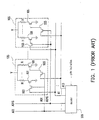
- FIG. 1 is an ink jet drive circuit disclosed in the U.S. Patent No. 6,299,292 .
- the drive circuit includes 16 printhead arrays 105.
- Each printhead array 105 includes 13 heating resistors (heaters) H.
- the decoder 109 After the decoder 109 receives the print command, it will send out the address decoding signal of the printhead based on the print command to heat up the heaters H corresponding to the specific addresses so that the ink will be heated and jetted out via the nozzle.
- the decoder 109 sends out the printhead array address signals AD1-AD16 and the heater address signals A1-A13.
- the printhead array address signals AD1-AD16 will determine which printhead array 105 will be driven.
- the heater address signals A1-A13 will determine which heater H in the specific printhead array 105 will heat the ink.
- the first terminal of the heater H receives the voltage signal V and the second terminal of the heater H will be controlled by two switches to determine whether current passes through that heater. These two switches comprise field-effect transistors 101 and 103.
- the gate of the field-effect transistor 103 receives the printhead array address signal; the source (when the field-effect transistors is a CMOS) receives the heater address signal.
- the drain when the field-effect transistor is a CMOS, will generate current signal and send it to the gate of the field-effect transistor 101.
- the source-drain of the field-effect transistor 101 will then be turned on when the voltage signal V is supplied, and the heater H will heat the ink and the ink is ready to be jetted out.
- FIG. 2 is the ink jet drive circuit disclosed in the U.S. Patent No. 5,867,183 .
- the ink jet drive circuit includes the ink jet printhead drive unit 201 and the printhead ink output units 211 and 213.
- the ink jet printhead drive unit 201 includes the ink jet printhead drive circuit 203 and the printhead selection circuit 205.
- the ink jet printhead drive circuit 203 outputs a set of bus control signals 207 and the printhead selection circuit 205 outputs a set of bus selection signal 209 selectively to enable one of the printhead ink output units.
- the control signals 207 and the corresponding selection signal will determine whether to enable the nozzles of one of the printhead ink output units.
- the printhead ink output unit 211 includes the enable circuit 215, nozzle firing circuits 225-231 and the nozzle 233.
- the enable circuit 215 includes a plurality of field-effect transistors 217, 219, 221 and 223.
- the drain (current input) of each field-effect transistor will receive the corresponding control signal in the bus control signal set 207.
- the gate (command input) of each field-effect transistor will receive the corresponding selection signal in the bus selection signal set 209.
- the source output terminal, current output
- the field-effect transistor 217 is coupled to the nozzle firing circuit 225 and the field-effect transistor 219 is coupled to the nozzle firing circuit 227. Then the nozzle firing circuit will jet out the ink out of the nozzle 223.
- the operating principle of the other printhead ink output unit 213 is the same as that of the above mentioned printhead ink output unit 211.
- An objective of the present invention is to provide an ink jet printhead control circuit which is capable of reducing the ink jetting delay, increasing the drive level, and improving the ink-jet performance.
- the present invention provides an ink jet printhead control circuit, which comprises a nozzle firing circuit and a nozzle firing control circuit.
- the nozzle firing circuit comprises a first switch and a heating resistor, wherein the first switch and the heating resistor are coupled in series between a power voltage level and a predetermined voltage level.
- the nozzle firing control circuit is coupled to the nozzle firing circuit to receive a selection signal and an address signal. When the address signal and the selection signal are enabled, the nozzle firing circuit is controlled to apply the power voltage level (when the power voltage level is at a high voltage level) to turn on the first switch, so that a current flows through the heating resistor.
- the predetermined voltage level is a ground voltage level.
- the first switch comprises a control terminal
- the nozzle firing control circuit comprises a second switch and a third switch.
- the second switch has a first terminal coupled to the power voltage level, and a second terminal coupled to the control terminal of the first switch.
- the third switch has a first terminal for receiving the selection signal, a second terminal coupled to the control terminal of the second switch, and a control terminal for receiving the address signal. When the address signal is enabled, the third switch is turned on.
- the nozzle firing control circuit further comprises a first impedance element and a second impedance element.
- the first impedance element has a terminal coupled to the control terminal of the first switch and the other terminal coupled to the predetermined voltage level.
- the second impedance element has a terminal coupled to the control terminal of the second switch and the other end coupled to the predetermined voltage level.
- each of the first impedance element and the second impedance element respectively comprises a resistor.
- the nozzle firing control circuit further comprises a fourth switch, a voltage dividing element, and a fifth switch.
- the fourth switch has a first terminal coupled to the control terminal of the first switch, and a second terminal coupled to the predetermined voltage level.
- the voltage dividing element has an input terminal for receiving the selection signal, and an output terminal coupled to the control terminal of the fourth switch, and is used to output a signal by dividing the voltage level of the selection signal.
- the fifth switch has a first terminal coupled to the output terminal of the voltage dividing element, a second terminal coupled to the predetermined voltage level, and a control terminal for receiving the address signal.
- the voltage dividing element comprises a third impedance element and a fourth impedance element.
- the third impedance element has a terminal which is the input terminal of the voltage dividing element, and the other terminal which is the output terminal of the voltage dividing element.
- the fourth impedance element has a terminal coupled to the output terminal of the voltage dividing element and the other terminal coupled to the predetermined voltage level.
- the third impedance element comprises a resistor, a sixth switch, and a seventh switch, wherein the resistor has one terminal for receiving the selection signal.
- the sixth switch has a first terminal for receiving the selection signal, a control terminal coupled to the other terminal of the resistor, and a second terminal coupled to the fourth impedance element.
- the seventh switch has a first terminal coupled to the other terminal of the resistor, a second terminal coupled to the predetermined voltage level, and a control terminal for receiving the address signal.
- each of the third impedance element and fourth impedance element respectively comprises a resistor.
- the nozzle firing control circuit further comprises a fifth impedance element.
- the fifth impedance element has a terminal coupled to the control terminal of the fifth switch and the other terminal coupled to the predetermined voltage level.
- the fifth impedance element comprises a resistor.
- the ink jet printhead control circuit further comprises a disable control circuit.
- the disable control circuit is coupled to the first switch for receiving the selection signal. When the selection signal is disabled, the first switch is controlled to be turned off.
- the first switch comprises a control terminal
- the disable control circuit comprises an eighth switch, a ninth switch, and a sixth impedance element.
- the eighth switch has a first terminal coupled to the control terminal of the first switch, and a second terminal coupled to the predetermined voltage level.
- the ninth switch has a first terminal coupled to the control terminal of the eighth switch, a second terminal coupled to the predetermined voltage level, and a control terminal for receiving the selection signal.
- the sixth impedance element has a terminal coupled to the power voltage level, and the other terminal coupled to the first terminal of the ninth switch.
- the sixth impedance element is a transistor having a drain and a gate coupled to the power voltage level and a source coupled to the first terminal of the ninth switch.
- the first switch comprises a first terminal coupled to the power voltage level, a second terminal coupled to the heating resistor, and a control terminal, wherein one terminal of the heating resistor is coupled to the second terminal of the first switch and the other terminal of the heating resistor is coupled to the predetermined voltage level.
- the first switch comprises a first terminal, a second terminal and a control terminal, wherein the first terminal is coupled to the predetermined voltage level, the second terminal coupled to the heating resistor, and one terminal of the heating resistor is coupled to the second terminal of the first switch and the other terminal of the heating resistor is coupled to the power voltage level.
- the predetermined voltage level is grounded or a ground voltage level.
- the address signal is used to drive the heating resistor (i.e. to control the status of the switch of the nozzle firing circuit), and thus the address signal requires a larger driving force, and ink jetting delay may occur.
- the present invention adopts the power voltage level to turn on the switch of the nozzle firing circuit, and then to drive the heating resistor, thus achieving the purpose of jetting ink.
- the delay time can be reduced, and the address signal output from the printer can drive the nozzle firing circuit with a small driving force.
- the present invention can also improve the printing quality of ink jet printers.
- FIG. 1 is a drive circuit of an ink jet printer of U.S. Patent No. US6,299,292 .
- FIG. 2 is a drive circuit of the ink jet printer of U.S. Patent No. US5,867,183 .
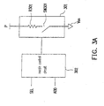
- FIG. 3A is a schematic circuit block diagram of the ink jet printhead control circuit according to the ink jet printhead control circuit of an embodiment of the present invention.
- FIGs. 3B ⁇ 3D are schematic circuit block diagrams of the ink jet printhead control circuit according to the ink jet printhead control circuit of another embodiment of the present invention.
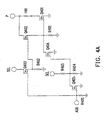
- FIGs. 4A and 4B are circuit diagrams of the ink jet printhead control circuit implemented according to the embodiment of FIG. 3A of the present invention.
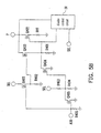
- FIGs. 5A and 5B are circuit diagrams of the ink jet printhead control circuit implemented according to the embodiment of FIGs. 4A and 4B of the present invention, respectively.
- FIGs. 5C and 5D are circuit diagrams of the ink jet printhead control circuit implemented according to the embodiment of FIGs. 5A and 5B of the present invention, respectively.
- FIGs. 6A and 6B are another circuit diagrams of the ink jet printhead control circuit implemented according to the embodiment of FIG. 3A of the present invention.
- FIGs. 6C and 6D are circuit diagrams of the ink jet printhead control circuit implemented according to the embodiment of FIGs. 6A and 6B of the present invention, respectively.
- FIGs. 7A and 7B are another circuit diagrams of the ink jet printhead control circuit implemented according to the embodiment of FIG. 3A of the present invention.
- FIGs. 7C and 7D are circuit diagrams of the ink jet printhead control circuit implemented according to the embodiment of FIGs. 7A and 7B of the present invention, respectively.
- FIGs. 8A and 8B are another circuit diagrams of the ink jet printhead control circuit implemented according to the embodiment of FIG. 3A of the present invention.
- the circuit architecture of the prior art adopts the address signal to drive the heating resistor (i.e. to control the status of the switch of the nozzle firing circuit), and thus the address signal requires a larger driving force to drive the nozzle firing circuit.
- a field-effect transistor is added between the address signal and the heating resistor of the firing circuit to function as a control switch.
- the transistor has a body effect, such that the drive level received by the firing circuit is relatively low, thus causing an ink-jetting delay.
- the present invention provides an ink jet printhead control circuit for reducing the ink jetting delay, increasing the drive level, and improving the ink-jet performance.
- the present invention is illustrated with embodiments herein blow.
- FIG. 3A is a schematic circuit block diagram of the ink jet printhead control circuit according to an embodiment of the present invention.
- an ink jet printhead ink output unit e.g., ink cartridge with printhead chip, or printhead chip itself
- the circuit comprises at least one nozzle firing circuit 301 and a nozzle firing control circuit 302.
- the nozzle firing circuit 301 at least comprises a switch SW301 and a heating resistor R301, wherein the switch SW301 and the heating resistor R301 are coupled in series between the power voltage level P and the predetermined voltage level Vss.
- the heating resistor is coupled to the power voltage level P
- the switch SW301 is coupled between the heating resistor and the predetermined voltage level Vss.
- the nozzle firing control circuit 302 is electrically coupled (“electrically coupled” or “electrically couple(s)” or “coupled” or “couple(s)” is referred to as “coupled” or “couple(s)” in the present invention) to the nozzle firing circuit 301, and receives a selection signal SEL and an address signal ADD.
- the nozzle firing circuit 301 is controlled to apply the power voltage level P (when the power voltage level is at a high voltage level) to turn on the switch SW301, so as to drive the heating resistor R301 to jet ink.
- the address signal and the selection signal have a high voltage level and a low voltage level. It is known to the person having ordinary skill in the art that the selection signal is used to select desired one or several of the printhead ink output units, and the address signal is used to selectively enable the specific group of nozzle firing circuits 301 that corresponds to the address signal.
- FIGs. 3B ⁇ 3D are several examples of applying the power voltage level P to turn on the switch SW301.
- N-type transistors are taken as an example to illustrate all switches, and it is apparent to those of ordinary skill in the art that in additional to the N-type transistors, P-type transistors, multiplexers, transmission gates, relays, etc. can also be implemented as the switches, and thus the present invention is not limited herein.
- a switch SW302 is electrically coupled between the power voltage level P and the switch SW301.
- the switch SW302 When the address signal ADD and the selection signal SEL are enabled, the switch SW302 is turned on, such that the control terminal (i.e., the gate of the N-type transistor) of the switch SW301 directly receives the power voltage level P, and an effect of rapid conduction can be obtained.
- FIG. 3C shows another embodiment of applying the power voltage level P to turn on the switch SW301.
- the power voltage level P is coupled to the control terminal (i.e., the gate of the N-type transistor) of the switch SW301 via the impedance element R302.
- the switch SW302 is further coupled in series under the impedance element R302.
- the switch SW302 When the address signal ADD or the selection signal SEL is not enabled, the switch SW302 is turned on, and when the address signal ADD and the selection signal SEL are enabled, the switch SW302 is controlled to be turned off (non-conducted), such that the control terminal of the switch SW301, i.e., the gate of the N-type transistor, receives the power voltage level P, thus achieving the effect of rapid conduction.
- the switch SW301 of the nozzle firing circuit 301 and the heating resistor R301 are coupled in series between the power voltage level P and the predetermined voltage level Vss, and when the address signal ADD and the selection signal SEL are enabled, the nozzle firing control circuit 302 controls the nozzle firing circuit 301 to apply the power voltage level P (when the power voltage level is at a high voltage level) to turn on the switch SW301, thus driving the heating resistor R301 to jet ink.
- FIGs. 4A and 4B are circuit diagrams of the ink jet printhead control circuit according to the embodiment of FIG. 3A of the present invention.
- the nozzle firing circuit 301 of the circuit employs a transistor Q401 as the switch SW301 and a resistor H41 as the heating resistor R301.
- the nozzle firing control circuit 302 of the circuit employs, for example, transistors Q402, Q403, Q404, and Q405 and resistors R401, R402, R403, R404, and R405, and the coupling relationship thereof is shown in FIG. 4A.
- the transistor Q402 When the selection signal SEL and address signal ADD are not enabled (the enabled state is assumed to be logic 1 in this embodiment), the transistor Q402 is turned off (non-conducted), and the transistor Q401 is also turned off, and thus no current passes through the heating resistor H41.
- the printer selects a certain ink cartridge having the ink jet printhead control circuit, however, the specific ink jet printhead control circuit in the selected certain ink cartridge is not selected or addressed (as an ink cartridge may contain a plurality of sets of ink jet printhead control circuits which are respectively coupled to the corresponding address signal ADD). At this condition, the transistors Q403 and Q405 are turned off, such that the Q402 is turned off.
- the selection signal SEL When the selection signal SEL is enabled, the Q404 is turned on, and the gate of the Q401 is drawn to a low voltage level to be turned off, such that the nozzle firing circuit does not jet ink.
- the printer does not select the ink cartridge having the ink jet printhead control circuit of this embodiment.
- the transistors Q402 and Q404 are turned off, and the transistor Q401 is also turned off, such that no current passes through the heating resistor H41.
- the selection signal SEL and the address signal ADD are enabled, the transistors Q403 and Q405 are turned on, and the transistor Q402 receives the selection signal SEL transmitted from the transistor Q403 to be turned on.
- the transistor Q404 is turned off as the voltage dividing point of the selection signal is drawn to a low voltage level by the transistor Q405. Since Q402 is turned on, the power voltage level P flows into the gate of the transistor Q401 (when the power voltage level P is at a high voltage level). Therefore, the transistor Q401 is quickly turned on, such that a current passes through the heating resistor H41 to heat the ink to jet ink. It should be noted that when the selection signal SEL and the address signal ADD are enabled and the power voltage level P is at a low voltage level (and the power supplied to the nozzle firing circuit is not sufficient), the gate of the transistor Q401 is not turned on, and thus no current passes through the heating resistor H41 to heat the ink to jet ink.
- the operational voltage when the selection signal SEL and the address signal ADD are enabled and the operational voltage when the power voltage level P is at a high voltage level are about 8V-20V, and the preferred operation voltage is about 10V-13V.
- the applicable resistance of the R403 is in a range of about 1k ⁇ 50k ⁇ , and the preferred resistance is in a range of about 10k ⁇ 20k ⁇ .
- the applicable resistance of the R401, R402, R404, and R405 is in a range of about 5k ⁇ 250k ⁇ , and the preferred resistance is in a range of about 35k ⁇ 100k ⁇ .
- the present invention is not limited to the above numeral values.
- FIG. 4B the difference between FIG. 4B and FIG. 4A lies in that the transistor Q401 of the FIG. 4B is coupled between the heating resistor H41 and the power voltage level P. It is apparent to those of ordinary skill in the art that the operation thereof is the same as that described above, and will not be described herein again.
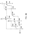
- FIGs. 5A and 5B are circuit diagrams of the ink jet printhead control circuit implemented according to the embodiment of FIGs. 4A and 4B of the present invention, respectively. Comparing FIG. 5A, FIG. 5B and FIG. 4A, FIG. 4B respectively, different from the circuit of FIGs. 4A and 4B, the circuits of FIGs. 5A and 5B further has a disable control circuit 51 coupled to the first switch SW301 for receiving the selection signal SEL. When the selection signal SEL is disabled, the first switch SW301 (transistor Q401) is controlled to be turned off.
- FIGs. 5C and 5D are circuit diagrams of the ink jet printhead control circuit implemented according to the embodiment of FIGs. 5A and 5B of the present invention, respectively.
- a disable control circuit 51 employs, for example, transistors Q506, Q507, and Q508, wherein the transistor Q506 is a transistor using an NMOS.
- the selection signal SEL is enabled (the enabled state is assumed to be logic 1 in this embodiment), the transistor Q507 is turned on and the voltage level at the node A50 is drawn to a low voltage level, such that the transistor Q508 is turned off.
- the transistor Q507 When the selection signal SEL is disabled, the transistor Q507 is turned off and the voltage level at the node A50 is a high voltage level (when the power voltage level P is a high voltage level), such that the transistor Q508 is turned on. Since the Q508 is turned on, the gate of the Q401 remains at a low voltage level, and thus the transistor Q401 can be protected from being interfered by noise and the problem of the ink cartridge jetting ink due to noise can be overcome.
- transistor Q506 can be equivalently replaced by a resistor, and the present invention is not limited to this.
- FIGs. 6A and 6B are another circuit diagrams of the ink jet printhead control circuit implemented according to the embodiment of FIG. 3A of the present invention. Comparing FIG. 6A and FIG. 4A, the difference between the circuits of FIG. 6A and FIG. 4A lies in that the resistor R403 of FIG. 4A is replaced by transistors Q605, Q606 and resistor R603 in FIG. 6A.
- the gates of the transistors Q606, Q403, Q402 are at a logic low voltage level and thus turned off.
- the gate of the transistor Q605 receives the high voltage level of the selection signal through the resistor R603, such that the transistor Q605 is turned on.
- the transistor Q404 is turned on, and the transistor Q401 is turned off.
- the selection signal SEL is not enabled and the address signal ADD is enabled, the transistors Q403, Q405, Q606 are turned on, the gates of the transistor Q402 and the transistor Q404 are turned off due to the logic low voltage level, and the transistor 401 is also turned off.
- the transistors Q403, Q606, and Q405 are turned on, and the transistors Q605 and Q404 are turned off.
- the gate of the transistor Q402 receives the high voltage level of the selection signal SEL and thus is turned on.
- the power voltage level P is transmitted to the gate of the transistor Q401 through the transistor Q402, such that the transistor Q401 is turned on. Since the transistor Q401 is turned on, a current flows from the power voltage level P through the heating resistor H41 to make the nozzle firing circuit jet ink.
- the operational voltage when the selection signal SEL and the address signal ADD are enabled and the operational voltage when the power voltage level P is at a high voltage level are about 8V-20V, and the preferred operation voltage is about 10V-13V.
- the applicable resistance of R401, R402, R404, and R405 is in a range of about 5k-250k ⁇ , and preferably about 35k ⁇ 100k ⁇ .
- the applicable resistance of R603 is in a range of about 100 ⁇ 10k ⁇ , and preferably about 100 ⁇ 1k ⁇ .
- the present invention is not limited to the above numeral values.
- the difference between the circuits of FIG. 6A and FIG. 6B lies in that the transistor Q401 of FIG. 6B is coupled between the heating resistor H41 and the power voltage level P. It is apparent to those of ordinary skill in the art that the operation thereof is also the same as that described above, and will not be described herein again.
- FIGs. 6C and 6D are circuit diagrams of the ink jet printhead control circuit implemented according to the embodiment of FIG. 6A and 6B of the present invention, respectively. Comparing FIG. 6C, FIG. 6D and FIG. 6A, FIG. 6B respectively, different from FIG. 6A and FIG. 6B, the circuits of FIG. 6C and FIG. 6D further comprises a disable control circuit 61.
- the implementation of the disable control circuit 61 is the same as that of FIG. 5C and FIG. 5D, and the operation thereof is also the same, and will not be described herein again.
- FIGs. 7A and 7B are another two circuit diagrams of the ink jet printhead control circuit implemented according to the embodiment of FIG. 3A of the present invention.
- the nozzle firing circuit 301 is implemented with a heating resistor H71 and a transistor Q701;
- the nozzle firing control circuit 302 is implemented with transistors Q702, Q703 and resistors R701, R702.
- the selection signal SEL is enabled and the address signal is not enabled, the transistor Q703 is turned off such that the Q702 is turned off, and thus the transistor Q701 is turned off, and the nozzle firing circuit 301 does not jet ink.
- the transistor Q703 When the selection signal SEL and the address signal are enabled, the transistor Q703 is turned on, the selection signal SEL turns on the transistor Q702 through the transistor Q703, and the power voltage level P (when the power voltage level is at a high voltage level) is transmitted to the gate of the transistor Q701 through the transistor Q702 to turn on the transistor Q701, such that the nozzle firing circuit 301 can heat the ink to jet ink.
- the operational voltage when the selection signal SEL and the address signal ADD are enabled and the operational voltage when the power voltage level P is at a high voltage level are about 8V-20V, and the preferred operation voltage is about 10V-13V.
- the applicable resistance of R701 and R702 is in a range of about 5k ⁇ 250k ⁇ , and preferably about 35k ⁇ 100k ⁇ . However, the present invention is not limited to this.
- FIGs. 7C and 7D are circuit diagrams of the ink jet printhead control circuit implemented according to the embodiment of FIG. 7A and FIG. 7B of the present invention, respectively. Comparing FIG. 7C, FIG. 7D and FIG. 7A, FIG. 7B respectively, different from FIG. 7A and FIG. 7B, the circuits of FIG. 7C and FIG. 7D further comprises a disable control circuit 71.
- the implementation of the disable control circuit 71 is the same as that of FIG. 5C and FIG. 5D, and the operation thereof is also the same, and will not be described herein.
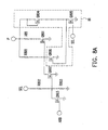
- FIGs. 8A and 8B are another two circuit diagrams of the ink jet printhead control circuit implemented according to the embodiment of FIG. 3A of the present invention.
- the nozzle firing circuit 301 is implemented with a heating resistor H81 and a transistor Q801;
- the nozzle firing control circuit 302 is implemented with transistors Q802, Q803, resistors R801, R802, R803, and a disable control circuit 81, wherein the disable control circuit 81 is implemented with transistors Q804, Q805, and Q806.
- the transistors Q802, Q803, and Q805 are turned off.
- the transistor Q806 is turned on such that the transistor Q801 is turned off, and thus no current passes through the heating resistor H81.
- the selection signal SEL is enabled and the address signal ADD is not enabled, the transistor Q805 is turned on such that the transistor Q806 is turned off.
- the selection signal SEL after being subjected to a voltage division by resistors R802 and R803, flows into the gate of the transistor Q802, so as to turn on the transistor Q802.
- the transistor Q801 is not turned on, and the nozzle firing circuit does not jet ink.
- the transistor Q803 is turned on such that the transistor Q802 is turned off.
- the power voltage level P (at a high voltage level) directly flows into the gate of the transistor Q401 through the resistor R801, such that the transistor Q401 is quickly turned on and thus a current passes through the heating resistor H81 to heat the ink to jet ink.
- the operational voltage when the selection signal SEL and the address signal ADD are enabled and the operational voltage when the power voltage level P is at a high voltage level are about 8V-20V, and the preferred operation voltage is about 10V-13V.
- the applicable resistance of R801 and R802 is in a range of about 1k ⁇ 50k ⁇ , and preferably about 10k ⁇ 20k ⁇ .
- the applicable resistance of R803 is in a range of about 5k ⁇ 250k ⁇ , and preferably about 35k ⁇ 100k ⁇ .
- the present invention is not limited to this.
- the present invention adopts the power voltage level P to turn on the switch SW301 of the nozzle firing circuit 301, and then drive the heating resistor R301, so as to heat the ink to jet ink.
- the driving force of power voltage level P is larger than that of the address signal ADD, and is quicker, so the delay time can be reduced, and the address signal output by the printer can also drive the nozzle firing circuit with a smaller driving force.
- the present invention can further improve the printing quality of the ink jet printer.
Landscapes
- Engineering & Computer Science (AREA)
- Microelectronics & Electronic Packaging (AREA)
- Particle Formation And Scattering Control In Inkjet Printers (AREA)
Applications Claiming Priority (1)
| Application Number | Priority Date | Filing Date | Title |
|---|---|---|---|
| CNA2006100786081A CN101062610A (zh) | 2006-04-26 | 2006-04-26 | 喷墨印头控制电路 |
Publications (2)
| Publication Number | Publication Date |
|---|---|
| EP1849604A2 true EP1849604A2 (fr) | 2007-10-31 |
| EP1849604A3 EP1849604A3 (fr) | 2008-09-17 |
Family
ID=38326872
Family Applications (1)
| Application Number | Title | Priority Date | Filing Date |
|---|---|---|---|
| EP07250143A Withdrawn EP1849604A3 (fr) | 2006-04-26 | 2007-01-15 | Circuit de commande de tête d'impression à jet d'encre |
Country Status (2)
| Country | Link |
|---|---|
| EP (1) | EP1849604A3 (fr) |
| CN (1) | CN101062610A (fr) |
Cited By (1)
| Publication number | Priority date | Publication date | Assignee | Title |
|---|---|---|---|---|
| EP3227121A4 (fr) * | 2014-12-02 | 2018-07-11 | Hewlett-Packard Development Company, L.P. | Tête d'impression |
Families Citing this family (1)
| Publication number | Priority date | Publication date | Assignee | Title |
|---|---|---|---|---|
| CN102795001B (zh) * | 2012-06-27 | 2014-09-03 | 杭州冲之上数码设备有限公司 | 一种应用于喷墨打印机的智能电源 |
Family Cites Families (3)
| Publication number | Priority date | Publication date | Assignee | Title |
|---|---|---|---|---|
| US5083137A (en) * | 1991-02-08 | 1992-01-21 | Hewlett-Packard Company | Energy control circuit for a thermal ink-jet printhead |
| DE69733295T2 (de) * | 1996-06-26 | 2006-02-02 | Canon K.K. | Aufzeichnungskopf und Aufzeichnungsapparat unter Verwendung derselben |
| JP2000141660A (ja) * | 1998-11-11 | 2000-05-23 | Canon Inc | 記録へッド及びその記録へッドを用いた記録装置 |
-
2006
- 2006-04-26 CN CNA2006100786081A patent/CN101062610A/zh active Pending
-
2007
- 2007-01-15 EP EP07250143A patent/EP1849604A3/fr not_active Withdrawn
Cited By (2)
| Publication number | Priority date | Publication date | Assignee | Title |
|---|---|---|---|---|
| EP3227121A4 (fr) * | 2014-12-02 | 2018-07-11 | Hewlett-Packard Development Company, L.P. | Tête d'impression |
| US10960661B2 (en) | 2014-12-02 | 2021-03-30 | Hewlett-Packard Development Company, L.P. | Fluid ejection device circuit |
Also Published As
| Publication number | Publication date |
|---|---|
| EP1849604A3 (fr) | 2008-09-17 |
| CN101062610A (zh) | 2007-10-31 |
Similar Documents
| Publication | Publication Date | Title |
|---|---|---|
| US5371530A (en) | Thermal ink jet printhead having a switched stand-by mode | |
| US8033626B2 (en) | Ink jet printhead module and ink jet printer | |
| US6471324B1 (en) | Printhead with malfunction prevention function and printing apparatus using it | |
| TWI435808B (zh) | 流體噴出裝置 | |
| EP1142715B1 (fr) | Tête d'impression et imprimante pourvue d'une telle tête | |
| US20040017414A1 (en) | Printhead and image printing apparatus | |
| US6286924B1 (en) | Apparatus and method for heating ink jet printhead | |
| US7547083B2 (en) | Ink jet printer with a plurality of printhead control units | |
| US6830307B2 (en) | Integrated circuit and drive scheme for an inkjet printhead | |
| US6712437B2 (en) | Printhead board, printhead and printing apparatus | |
| EP1849604A2 (fr) | Circuit de commande de tête d'impression à jet d'encre | |
| US8506030B2 (en) | Element substrate, printhead, and head cartridge | |
| JP4035253B2 (ja) | 記録ヘッド及びその記録ヘッドを用いた記録装置 | |
| JP2006159780A (ja) | インクジェット記録ヘッド用基板と駆動制御方法、インクジェット記録ヘッド、インクジェット記録ヘッドカートリッジ及びインクジェット記録装置 | |
| US20070242092A1 (en) | Ink jet Printhead Control Circuit | |
| JPH1034898A (ja) | 記録ヘッド及びその記録ヘッドを用いた記録装置 | |
| EP1600295B1 (fr) | Contrôleur de tête d'impression et imprimante à jet d'encre | |
| US7661784B2 (en) | Methods and apparatus for control of a signal in a printing apparatus | |
| JP4532890B2 (ja) | 記録ヘッドおよび該記録ヘッドを備えた記録装置 | |
| JP7465084B2 (ja) | 素子基板、液体吐出ヘッド、及び記録装置 | |
| CN100503247C (zh) | 喷墨印头控制器及喷墨打印机 | |
| CN101190603A (zh) | 三维式喷墨驱动电路及喷墨驱动矩阵电路 | |
| CN100400291C (zh) | 喷墨头控制电路 | |
| CN106965556A (zh) | 喷墨控制电路 | |
| JP2000037870A (ja) | 記録ヘッド及び記録装置 |
Legal Events
| Date | Code | Title | Description |
|---|---|---|---|
| PUAI | Public reference made under article 153(3) epc to a published international application that has entered the european phase |
Free format text: ORIGINAL CODE: 0009012 |
|
| 17P | Request for examination filed |
Effective date: 20070119 |
|
| AK | Designated contracting states |
Kind code of ref document: A2 Designated state(s): AT BE BG CH CY CZ DE DK EE ES FI FR GB GR HU IE IS IT LI LT LU LV MC NL PL PT RO SE SI SK TR |
|
| AX | Request for extension of the european patent |
Extension state: AL BA HR MK YU |
|
| PUAL | Search report despatched |
Free format text: ORIGINAL CODE: 0009013 |
|
| AK | Designated contracting states |
Kind code of ref document: A3 Designated state(s): AT BE BG CH CY CZ DE DK EE ES FI FR GB GR HU IE IS IT LI LT LU LV MC NL PL PT RO SE SI SK TR |
|
| AX | Request for extension of the european patent |
Extension state: AL BA HR MK RS |
|
| AKX | Designation fees paid | ||
| REG | Reference to a national code |
Ref country code: DE Ref legal event code: 8566 |
|
| STAA | Information on the status of an ep patent application or granted ep patent |
Free format text: STATUS: THE APPLICATION IS DEEMED TO BE WITHDRAWN |
|
| 18D | Application deemed to be withdrawn |
Effective date: 20090318 |