EP1850141A2 - Appareil et procédé pour le traitement de signaux entre un testeur et une pluralité de dispositifs à l'essai à températures élevées et avec toucher unique d'un réseau de sondes - Google Patents
Appareil et procédé pour le traitement de signaux entre un testeur et une pluralité de dispositifs à l'essai à températures élevées et avec toucher unique d'un réseau de sondes Download PDFInfo
- Publication number
- EP1850141A2 EP1850141A2 EP07008318A EP07008318A EP1850141A2 EP 1850141 A2 EP1850141 A2 EP 1850141A2 EP 07008318 A EP07008318 A EP 07008318A EP 07008318 A EP07008318 A EP 07008318A EP 1850141 A2 EP1850141 A2 EP 1850141A2
- Authority
- EP
- European Patent Office
- Prior art keywords
- under test
- devices under
- tester
- multichip module
- micro
- Prior art date
- Legal status (The legal status is an assumption and is not a legal conclusion. Google has not performed a legal analysis and makes no representation as to the accuracy of the status listed.)
- Withdrawn
Links
Images

Classifications
-
- G—PHYSICS
- G01—MEASURING; TESTING
- G01R—MEASURING ELECTRIC VARIABLES; MEASURING MAGNETIC VARIABLES
- G01R31/00—Arrangements for testing electric properties; Arrangements for locating electric faults; Arrangements for electrical testing characterised by what is being tested not provided for elsewhere
- G01R31/28—Testing of electronic circuits, e.g. by signal tracer
- G01R31/2851—Testing of integrated circuits [IC]
- G01R31/2886—Features relating to contacting the IC under test, e.g. probe heads; chucks
- G01R31/2889—Interfaces, e.g. between probe and tester
-
- H—ELECTRICITY
- H10—SEMICONDUCTOR DEVICES; ELECTRIC SOLID-STATE DEVICES NOT OTHERWISE PROVIDED FOR
- H10P—GENERIC PROCESSES OR APPARATUS FOR THE MANUFACTURE OR TREATMENT OF DEVICES COVERED BY CLASS H10
- H10P74/00—Testing or measuring during manufacture or treatment of wafers, substrates or devices
Definitions
- Mechanical relays are also quite expensive. For example, the typical mechanical relays may each cost about $8.00. This may limit the return on investment (ROI) for the customer. Mechanical relays are generally rated for about 1 to 10 million test cycles. This may create reliability issues for the customer over time. Furthermore, mechanical relays are only rated for operation up to 85° C. This allows testing of NAND devices using mechanical relays at or below 85° C.
- ROI return on investment
- apparatus for processing signals between a tester and a plurality of devices under test, the apparatus comprising at least one multichip module, each of the at least one multichip module comprising a plurality of micro-electromechanical switches between a first set of connectors to the tester and a second set of connectors to the plurality of devices under test; and at least one driver to selectively operate each of the plurality of micro-electromechanical switches.
- a system for testing a plurality of devices under test comprising a set of tester electronics to generate signals for application to the plurality of devices under test, and to receive signals generated by the plurality of devices under test; a probe card with at least one multichip module mounted thereon, each of the at least one multichip module comprising a plurality of micro-electromechanical switches between a first set of connectors to the set of tester electronics and a second set of connectors to the plurality of devices under test, and a driver to selectively operate each of the plurality of micro-electromechanical switches; and a probe array to transmit signals between the at least one multichip module of the probe card and the plurality of devices under test.
- apparatus for processing signals between a tester and a plurality of devices under test comprising at least one multichip module mounted directly on a probe card and operable at a temperature of at least 125° C, and each of the at least one multichip module having a plurality of micro-electromechanical switches between a first set of connectors to the tester and a second set of connectors to the plurality of devices under test.
- a method of processing signals between a tester and a plurality of devices under test comprising connecting the tester and the plurality of devices under test with at least one multichip module, each of the at least one multichip module having a plurality of micro-electromechanical switches between a first set of connectors to the tester and a second set of connectors to the plurality of devices under test; and selectively operating each of the plurality of micro-electromechanical switches.
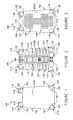
- FIGURES 1-3 illustrate one exemplary embodiment of a multichip module for processing signals between a tester and a plurality of devices under test
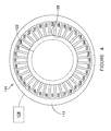
- FIGURE 4 illustrates a system having a probe card with a plurality of multichip modules for processing signals between a tester and a plurality of devices under test;
- FIGURES 5-7 illustrate another exemplary embodiment of a multichip module for processing signals between a tester and a plurality of devices under test.
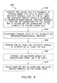
- FIGURE 8 is a flow chart diagram illustrative of methods of processing signals between a tester and a plurality of devices under test.
- apparatus 100 for processing signals may include a configuration in which each of multichip modules 102 are mounted directly on a probe card 112. Due to the proximity of multichip modules 102 to probe card 112 and the devices under test (not shown), one or more of multichip modules 102 may operate at a speed of at least 100 MHz. In another embodiment, one or more of multichip modules 102 may operate at a speed above 20 MHz to about 100 MHz.
- one or more of multichip modules 102 may be rated for at least 1 billion test cycles. Multichip modules 102 may be rated for 10 billion or more test cycles. This is due, at least in part, to the micro-electromechanical switches 104 that may be used instead of other types of switches.
- MEM MCM 102 may be attached to probe card 112 using screws 120 or other fasteners, a new tester does not need to be purchased from a supplier of the ATE system. A customer may simply design a probe care and attach these MEM MCMs to the probe card and install this new probe card assembly onto an existing ATE system.
- one or more of drivers 110 may designed to supply an electrostatic potential to selectively activate a MEMs gate associated with one or more of the plurality of micro-electromechanical switches 104.
- One or more of drivers 110 may be a vacuum-florescent display driver die 110.
- four drivers 110 (FIGURE 2) act as an algorithmic pattern generating system (APGS) and supply the electrostatic potential to four separate DUTs independently of one another.
- one driver 110 (FIGURE 6) acts as an algorithmic pattern generating system (APGS) and supplies electrostatic potential to DUTs.
- the second set of connectors of multichip modules 102 attach to a probe array 122.
- This probe array 122 may have at least 6000 probe tip needles so as to test at least 6000 test sites of the plurality of devices under test during a single touchdown of probe array 122.
- each multichip module 102 may test 12 DUTs, there may be 36 multichip modules in attachment to probe card 112 for a total of 432 DUTs, and there may be 16 test sites on each one of the DUTs for a total of 6912 test sites, which in turn requires 6912 probe tip needles.
- System 124 may include a set of tester electronics 126 to generate signals for application to the plurality of devices under test, and to receive signals generated by the plurality of devices under test.
- System 124 may include probe card 112 with at least one multichip module 102 mounted directly on probe card 112.
- Each of the at least one multichip module 102 may include a plurality of micro-electromechanical switches 104 between a first set of connectors to the set of tester electronics 126 and a second set of connectors to the plurality of devices under test.
- System may include one or more drivers 110 to selectively operate each of the plurality of micro-electromechanical switches 104.
- System 124 may further include probe array 122 to transmit signals between the multichip modules 102 of probe card 112 and the plurality of devices under test.
- Probe card 112 may have a maximum diameter of 440 millimeters. Probe card 112 may form an opening 128 for probe array 122. In an embodiment, opening 128 has a minimum diameter of 330 millimeters. Probe card 112 may contains at least 36 of multichip modules 102 mounted thereon.
- probe array 112 may have at least 6000 probe tip needles so as to test at least 6000 test sites of the plurality of devices under test during a single touchdown of probe array 112.
- system 124 enables one touchdown testing of 300 mm wafers containing NAND devices to be tested up to 100 MHz by mounting micro-electromechanical multichip modules 102 very close to the DUTs. This one touchdown testing cannot be achieved by using mechanical relays or active silicon devices mounted on daughter boards. Daughter boards mounted on the probe cannot achieve the required density of switches because of the space required for connectors. Mechanical relays, which are mounted far from the DUTs, are generally limited to about 20 MHz and cannot achieve a data rate near 100 MHz.
- MCM multichip module
- MCM multichip module
- MEM MCMs 102 may be fabricated quite inexpensively. For example, an MCM package containing 128 SPDT switches with only 780 pins may cost about $300 per package. This drastically improves the return on investment (ROI) for the customer.
- ROI return on investment
- NAND devices may only be tested up to 85° C. However, using system 100, NAND devices may be tested at temperatures ranging from -40° C to 125° C with one or more of MEM MCMs 102.
- MEM MCMs 102 are generally mounted very close to the DUTs so as to increase the maximum data rate for testing NAND devices from 20 MHz to 100 MHz, and also to enable testing of the entire 300 mm wafer with one touchdown.
- MEM MCMs 102 Utilizing MEM MCMs 102 instead of mechanical relays is also more cost effective and more reliable.
- a typical mechanical relay is rated for 1-10 million cycles.
- a typical MEM MCM 102 may be rated for 1-10 billion cycles.
- Using daughter boards limits the density of switches that can be mounted on the probe card due to the space required for connectors.
- Multichip modules 102 are generally capable of much higher densities than daughter cards. Mounting multichip modules 102 onto probe card 112 enables the customer to double the pin count of the test system when testing NAND devices without buying a new ATE system.
- MCM substrate 102B may be a blind and buried via substrate made of NELCO 4000-13 Si, which is a typical MCM substrate.
- Connectors 106 and connectors 108 may include, but are not limited to pins. Such pins of the package may include Be-Cu springs that are attached with silver epoxy to the bottom of the NELCO 4000-13 Si substrate.
- MEMs 104 and single VFD 110 may be located inside MCM 102 and may be wired bond or soldered to the substrate.
- MCMs 102 may be reusable. MCMs 102 can be transferred form one probe card to another when the probe card becomes damaged or is simply obsolete due to a change in die size or layout on the wafers.
- Alignment pins 130 may be provided to align MCM 102 to probe card 112.
- Method 800 may include connecting 802 the tester and the plurality of devices under test with at least one multichip module, each of the at least one multichip module having a plurality of micro-electromechanical switches between a first set of connectors to the tester and a second set of connectors to the plurality of devices under test.
- Method 800 may include selectively operating 804 each of the plurality of micro-electromechanical switches.
- method 800 may further include operating 806 the at least one multichip module at a speed of at least 100 MHz. In an embodiment, method 800 may include operating 808 the multichip module at temperatures from -40° C to 125° C.
- Method 800 may include mounting 810 each of the at least one multichip module directly on the probe card.
Landscapes
- Engineering & Computer Science (AREA)
- Computer Hardware Design (AREA)
- Microelectronics & Electronic Packaging (AREA)
- General Engineering & Computer Science (AREA)
- Physics & Mathematics (AREA)
- General Physics & Mathematics (AREA)
- Testing Or Measuring Of Semiconductors Or The Like (AREA)
- Tests Of Electronic Circuits (AREA)
Applications Claiming Priority (1)
| Application Number | Priority Date | Filing Date | Title |
|---|---|---|---|
| US11/410,699 US7859277B2 (en) | 2006-04-24 | 2006-04-24 | Apparatus, systems and methods for processing signals between a tester and a plurality of devices under test at high temperatures and with single touchdown of a probe array |
Publications (1)
| Publication Number | Publication Date |
|---|---|
| EP1850141A2 true EP1850141A2 (fr) | 2007-10-31 |
Family
ID=38353852
Family Applications (1)
| Application Number | Title | Priority Date | Filing Date |
|---|---|---|---|
| EP07008318A Withdrawn EP1850141A2 (fr) | 2006-04-24 | 2007-04-24 | Appareil et procédé pour le traitement de signaux entre un testeur et une pluralité de dispositifs à l'essai à températures élevées et avec toucher unique d'un réseau de sondes |
Country Status (6)
| Country | Link |
|---|---|
| US (2) | US7859277B2 (fr) |
| EP (1) | EP1850141A2 (fr) |
| JP (1) | JP2007292758A (fr) |
| KR (1) | KR101342178B1 (fr) |
| CN (1) | CN101063704B (fr) |
| TW (1) | TWI426281B (fr) |
Families Citing this family (12)
| Publication number | Priority date | Publication date | Assignee | Title |
|---|---|---|---|---|
| US7573276B2 (en) * | 2006-11-03 | 2009-08-11 | Micron Technology, Inc. | Probe card layout |
| US20080238461A1 (en) * | 2007-04-02 | 2008-10-02 | Ken Skala | Multi-type test interface system and method |
| US8305098B2 (en) * | 2007-04-26 | 2012-11-06 | Advantest (Singapore) Pte Ltd | Element usable with the method, and a standalone probe card tester formable using the method |
| US7612971B2 (en) * | 2007-06-15 | 2009-11-03 | General Electric Company | Micro-electromechanical system based switching in heating-ventilation-air-conditioning systems |
| WO2009147724A1 (fr) * | 2008-06-02 | 2009-12-10 | 株式会社アドバンテスト | Unité de plaquette de test et système de test |
| EP2336837B1 (fr) * | 2009-12-17 | 2012-09-12 | Electrolux Home Products Corporation N.V. | Ensemble électrique pour le fonctionnement sélectif d'un appareil domestique dans un mode de démonstration ou mode standard |
| US9753081B2 (en) * | 2010-02-05 | 2017-09-05 | Celerint, Llc | Muxing interface platform for multiplexed handlers to reduce index time system and method |
| TWI500945B (zh) * | 2013-12-17 | 2015-09-21 | Primax Electronics Ltd | 電路板之測試系統 |
| US11266344B2 (en) | 2016-09-21 | 2022-03-08 | Samsung Electronics Co., Ltd. | Method for measuring skin condition and electronic device therefor |
| US12099085B2 (en) | 2021-05-18 | 2024-09-24 | Analog Devices International Unlimited Company | Apparatuses and methods for testing semiconductor circuitry using microelectromechanical systems switches |
| CN113791251B (zh) * | 2021-11-15 | 2022-03-29 | 新恒汇电子股份有限公司 | 用于sim卡失效检测的方法、装置及产品 |
| WO2025003771A1 (fr) * | 2023-06-29 | 2025-01-02 | Inziv Ltd. | Inspection rapide d'un dispositif sous test |
Family Cites Families (31)
| Publication number | Priority date | Publication date | Assignee | Title |
|---|---|---|---|---|
| JPH0316930A (ja) * | 1989-06-13 | 1991-01-24 | Fujikura Ltd | 複雑屈折率分布を有する光ファイバの製造方法 |
| WO1996013967A1 (fr) * | 1994-10-28 | 1996-05-09 | Micromodule Systems | Dispositif d'essai electronique a haute densite et programmable |
| US5736850A (en) * | 1995-09-11 | 1998-04-07 | Teradyne, Inc. | Configurable probe card for automatic test equipment |
| US5834975A (en) * | 1997-03-12 | 1998-11-10 | Rockwell Science Center, Llc | Integrated variable gain power amplifier and method |
| US6119255A (en) * | 1998-01-21 | 2000-09-12 | Micron Technology, Inc. | Testing system for evaluating integrated circuits, a burn-in testing system, and a method for testing an integrated circuit |
| US6098142A (en) * | 1998-08-25 | 2000-08-01 | Leggett; John D. | Apparatus and method for using a communications port in polling mode and without interrupts |
| US6706546B2 (en) * | 1998-10-09 | 2004-03-16 | Fujitsu Limited | Optical reflective structures and method for making |
| US6499121B1 (en) * | 1999-03-01 | 2002-12-24 | Formfactor, Inc. | Distributed interface for parallel testing of multiple devices using a single tester channel |
| US6657455B2 (en) * | 2000-01-18 | 2003-12-02 | Formfactor, Inc. | Predictive, adaptive power supply for an integrated circuit under test |
| US6801869B2 (en) * | 2000-02-22 | 2004-10-05 | Mccord Don | Method and system for wafer and device-level testing of an integrated circuit |
| US6303885B1 (en) * | 2000-03-03 | 2001-10-16 | Optical Coating Laboratory, Inc. | Bi-stable micro switch |
| US6335224B1 (en) * | 2000-05-16 | 2002-01-01 | Sandia Corporation | Protection of microelectronic devices during packaging |
| US6396711B1 (en) * | 2000-06-06 | 2002-05-28 | Agere Systems Guardian Corp. | Interconnecting micromechanical devices |
| US6490536B1 (en) * | 2000-09-14 | 2002-12-03 | Lam Research Corporation | Integrated load simulator |
| DE10112364A1 (de) * | 2001-03-15 | 2002-09-19 | Hilti Ag | Handwerkzeuggerät mit elektronischem Tiefenanschlag |
| US6773962B2 (en) * | 2001-03-15 | 2004-08-10 | General Electric Company | Microelectromechanical system device packaging method |
| US6492798B2 (en) * | 2001-04-27 | 2002-12-10 | Logicvision, Inc. | Method and circuit for testing high frequency mixed signal circuits with low frequency signals |
| US6762612B2 (en) * | 2001-06-20 | 2004-07-13 | Advantest Corp. | Probe contact system having planarity adjustment mechanism |
| JP4064921B2 (ja) * | 2001-08-10 | 2008-03-19 | 株式会社アドバンテスト | プローブモジュール及び試験装置 |
| WO2003042094A2 (fr) * | 2001-11-09 | 2003-05-22 | Movaz Networks, Inc. | Module multipuce comprenant un reseau de miroirs mems a elements electroniques |
| US20040016995A1 (en) * | 2002-07-25 | 2004-01-29 | Kuo Shun Meen | MEMS control chip integration |
| US6882256B1 (en) * | 2003-06-20 | 2005-04-19 | Northrop Grumman Corporation | Anchorless electrostatically activated micro electromechanical system switch |
| US7068220B2 (en) * | 2003-09-29 | 2006-06-27 | Rockwell Scientific Licensing, Llc | Low loss RF phase shifter with flip-chip mounted MEMS interconnection |
| TWM253771U (en) * | 2004-03-11 | 2004-12-21 | Chipmos Technologies Inc | Low noise probe head |
| US7305571B2 (en) * | 2004-09-14 | 2007-12-04 | International Business Machines Corporation | Power network reconfiguration using MEM switches |
| US7091765B2 (en) * | 2004-09-30 | 2006-08-15 | International Business Machines Corporation | Circuit power reduction using micro-electromechanical switches |
| US7245134B2 (en) * | 2005-01-31 | 2007-07-17 | Formfactor, Inc. | Probe card assembly including a programmable device to selectively route signals from channels of a test system controller to probes |
| CN101151540B (zh) * | 2005-03-31 | 2010-07-21 | 奥克泰克有限公司 | 微小结构体的探针卡、微小结构体的检查装置以及检查方法 |
| US7285968B2 (en) * | 2005-04-19 | 2007-10-23 | Formfactor, Inc. | Apparatus and method for managing thermally induced motion of a probe card assembly |
| US7504841B2 (en) * | 2005-05-17 | 2009-03-17 | Analog Devices, Inc. | High-impedance attenuator |
| US7924035B2 (en) * | 2008-07-15 | 2011-04-12 | Formfactor, Inc. | Probe card assembly for electronic device testing with DC test resource sharing |
-
2006
- 2006-04-24 US US11/410,699 patent/US7859277B2/en not_active Expired - Lifetime
-
2007
- 2007-04-20 JP JP2007111672A patent/JP2007292758A/ja active Pending
- 2007-04-23 KR KR1020070039249A patent/KR101342178B1/ko active Active
- 2007-04-23 TW TW096114242A patent/TWI426281B/zh active
- 2007-04-24 EP EP07008318A patent/EP1850141A2/fr not_active Withdrawn
- 2007-04-24 CN CN2007101017137A patent/CN101063704B/zh active Active
-
2010
- 2010-12-21 US US12/974,950 patent/US20110089966A1/en not_active Abandoned
Also Published As
| Publication number | Publication date |
|---|---|
| TWI426281B (zh) | 2014-02-11 |
| KR101342178B1 (ko) | 2013-12-16 |
| CN101063704B (zh) | 2012-02-08 |
| CN101063704A (zh) | 2007-10-31 |
| JP2007292758A (ja) | 2007-11-08 |
| KR20070104851A (ko) | 2007-10-29 |
| US20070247140A1 (en) | 2007-10-25 |
| US7859277B2 (en) | 2010-12-28 |
| US20110089966A1 (en) | 2011-04-21 |
| TW200809233A (en) | 2008-02-16 |
Similar Documents
| Publication | Publication Date | Title |
|---|---|---|
| US20110089966A1 (en) | Apparatus and systems for processing signals between a tester and a plurality of devices under test | |
| US7046027B2 (en) | Interface apparatus for semiconductor device tester | |
| TWI424180B (zh) | 配接器框架 | |
| US12625178B2 (en) | Automatic test equipment | |
| US7129730B2 (en) | Probe card assembly | |
| JP2014508944A (ja) | 電子部品を自動試験/検証するための装置 | |
| US5001422A (en) | VLSI tester backplane | |
| JP2016524137A (ja) | 電子デバイスを試験するためのプローブカードアセンブリ | |
| JP2009541715A (ja) | プローブ・カード基板上のタイル角部のソーイング | |
| KR20140131481A (ko) | 포고 핀의 연결에 기계적 고정을 제공하는 테스트 소켓 | |
| KR100720788B1 (ko) | 인쇄 회로 기판을 이용해 칩을 테스트하기 위한 장치 | |
| US10962565B2 (en) | Substrate inspection apparatus | |
| US4488111A (en) | Coupling devices for operations such as testing | |
| US9063170B2 (en) | Interface for a test system | |
| KR100478261B1 (ko) | 반도체 기판 시험장치 | |
| KR101540239B1 (ko) | 프로브 조립체 및 프로브 기판 | |
| US20140253165A1 (en) | Probe card | |
| US12578382B2 (en) | Automatic test equipment including multiple pin electronics integrated circuits in form of module | |
| KR20240013658A (ko) | 자동 시험 장치 및 그 인터페이스 장치 | |
| JPH09252031A (ja) | ウェハテスタ | |
| US7352197B1 (en) | Octal/quad site docking compatibility for package test handler | |
| US12553941B2 (en) | Automatic test equipment | |
| US8203356B2 (en) | Device, system and method for testing and analyzing integrated circuits | |
| KR100253278B1 (ko) | 집적회로 테스트용 소켓 | |
| JPH1082825A (ja) | 半導体検査装置及び方法 |
Legal Events
| Date | Code | Title | Description |
|---|---|---|---|
| PUAI | Public reference made under article 153(3) epc to a published international application that has entered the european phase |
Free format text: ORIGINAL CODE: 0009012 |
|
| AK | Designated contracting states |
Kind code of ref document: A2 Designated state(s): AT BE BG CH CY CZ DE DK EE ES FI FR GB GR HU IE IS IT LI LT LU LV MC MT NL PL PT RO SE SI SK TR |
|
| AX | Request for extension of the european patent |
Extension state: AL BA HR MK YU |
|
| RIN1 | Information on inventor provided before grant (corrected) |
Inventor name: ANDBERG, JOHN Inventor name: DE LA PUENTE, EDMUNDO Inventor name: MAYDER, ROMI Inventor name: STELLMACHER, PAM |
|
| STAA | Information on the status of an ep patent application or granted ep patent |
Free format text: STATUS: THE APPLICATION IS DEEMED TO BE WITHDRAWN |
|
| 18D | Application deemed to be withdrawn |
Effective date: 20101102 |