EP1850364A2 - Plasmaanzeigetafel - Google Patents
Plasmaanzeigetafel Download PDFInfo
- Publication number
- EP1850364A2 EP1850364A2 EP07109455A EP07109455A EP1850364A2 EP 1850364 A2 EP1850364 A2 EP 1850364A2 EP 07109455 A EP07109455 A EP 07109455A EP 07109455 A EP07109455 A EP 07109455A EP 1850364 A2 EP1850364 A2 EP 1850364A2
- Authority
- EP
- European Patent Office
- Prior art keywords
- black matrix
- display panel
- plasma display
- organics
- weight percent
- Prior art date
- Legal status (The legal status is an assumption and is not a legal conclusion. Google has not performed a legal analysis and makes no representation as to the accuracy of the status listed.)
- Withdrawn
Links
- 239000011159 matrix material Substances 0.000 claims abstract description 138
- 239000000203 mixture Substances 0.000 claims abstract description 45
- 239000000758 substrate Substances 0.000 claims abstract description 22
- 239000000178 monomer Substances 0.000 claims description 37
- UHESRSKEBRADOO-UHFFFAOYSA-N ethyl carbamate;prop-2-enoic acid Chemical compound OC(=O)C=C.CCOC(N)=O UHESRSKEBRADOO-UHFFFAOYSA-N 0.000 claims description 23
- 239000001023 inorganic pigment Substances 0.000 claims description 22
- 229920000058 polyacrylate Polymers 0.000 claims description 19
- 239000003999 initiator Substances 0.000 claims description 18
- 239000000843 powder Substances 0.000 claims description 18
- 239000011521 glass Substances 0.000 claims description 17
- 239000002002 slurry Substances 0.000 claims description 12
- 239000003795 chemical substances by application Substances 0.000 claims description 7
- 239000006185 dispersion Substances 0.000 claims description 6
- BLRPTPMANUNPDV-UHFFFAOYSA-N Silane Chemical compound [SiH4] BLRPTPMANUNPDV-UHFFFAOYSA-N 0.000 claims description 5
- 229910000077 silane Inorganic materials 0.000 claims description 5
- 239000002518 antifoaming agent Substances 0.000 claims description 3
- 239000007822 coupling agent Substances 0.000 claims description 3
- 239000002270 dispersing agent Substances 0.000 claims description 3
- 238000002372 labelling Methods 0.000 claims description 3
- 239000004014 plasticizer Substances 0.000 claims description 3
- 150000001875 compounds Chemical class 0.000 description 11
- NIXOWILDQLNWCW-UHFFFAOYSA-M acrylate group Chemical group C(C=C)(=O)[O-] NIXOWILDQLNWCW-UHFFFAOYSA-M 0.000 description 10
- 230000007423 decrease Effects 0.000 description 9
- CERQOIWHTDAKMF-UHFFFAOYSA-N Methacrylic acid Chemical compound CC(=C)C(O)=O CERQOIWHTDAKMF-UHFFFAOYSA-N 0.000 description 5
- 125000001797 benzyl group Chemical group [H]C1=C([H])C([H])=C(C([H])=C1[H])C([H])([H])* 0.000 description 5
- 229920001897 terpolymer Polymers 0.000 description 5
- WMWLMWRWZQELOS-UHFFFAOYSA-N bismuth(iii) oxide Chemical compound O=[Bi]O[Bi]=O WMWLMWRWZQELOS-UHFFFAOYSA-N 0.000 description 4
- 239000000463 material Substances 0.000 description 4
- 239000002904 solvent Substances 0.000 description 4
- 229920002818 (Hydroxyethyl)methacrylate Polymers 0.000 description 3
- VFZKVQVQOMDJEG-UHFFFAOYSA-N 2-prop-2-enoyloxypropyl prop-2-enoate Chemical compound C=CC(=O)OC(C)COC(=O)C=C VFZKVQVQOMDJEG-UHFFFAOYSA-N 0.000 description 3
- WOBHKFSMXKNTIM-UHFFFAOYSA-N Hydroxyethyl methacrylate Chemical compound CC(=C)C(=O)OCCO WOBHKFSMXKNTIM-UHFFFAOYSA-N 0.000 description 3
- 239000004721 Polyphenylene oxide Substances 0.000 description 3
- MPIAGWXWVAHQBB-UHFFFAOYSA-N [3-prop-2-enoyloxy-2-[[3-prop-2-enoyloxy-2,2-bis(prop-2-enoyloxymethyl)propoxy]methyl]-2-(prop-2-enoyloxymethyl)propyl] prop-2-enoate Chemical compound C=CC(=O)OCC(COC(=O)C=C)(COC(=O)C=C)COCC(COC(=O)C=C)(COC(=O)C=C)COC(=O)C=C MPIAGWXWVAHQBB-UHFFFAOYSA-N 0.000 description 3
- UBEWDCMIDFGDOO-UHFFFAOYSA-N cobalt(II,III) oxide Inorganic materials [O-2].[O-2].[O-2].[O-2].[Co+2].[Co+3].[Co+3] UBEWDCMIDFGDOO-UHFFFAOYSA-N 0.000 description 3
- 239000011261 inert gas Substances 0.000 description 3
- 229920000570 polyether Polymers 0.000 description 3
- 229920005862 polyol Polymers 0.000 description 3
- 150000003077 polyols Chemical class 0.000 description 3
- VVQNEPGJFQJSBK-UHFFFAOYSA-N Methyl methacrylate Chemical compound COC(=O)C(C)=C VVQNEPGJFQJSBK-UHFFFAOYSA-N 0.000 description 2
- HVVWZTWDBSEWIH-UHFFFAOYSA-N [2-(hydroxymethyl)-3-prop-2-enoyloxy-2-(prop-2-enoyloxymethyl)propyl] prop-2-enoate Chemical compound C=CC(=O)OCC(CO)(COC(=O)C=C)COC(=O)C=C HVVWZTWDBSEWIH-UHFFFAOYSA-N 0.000 description 2
- 230000002159 abnormal effect Effects 0.000 description 2
- NIXOWILDQLNWCW-UHFFFAOYSA-N acrylic acid group Chemical group C(C=C)(=O)O NIXOWILDQLNWCW-UHFFFAOYSA-N 0.000 description 2
- 125000001931 aliphatic group Chemical group 0.000 description 2
- 239000003513 alkali Substances 0.000 description 2
- 230000004888 barrier function Effects 0.000 description 2
- RWCCWEUUXYIKHB-UHFFFAOYSA-N benzophenone Chemical compound C=1C=CC=CC=1C(=O)C1=CC=CC=C1 RWCCWEUUXYIKHB-UHFFFAOYSA-N 0.000 description 2
- 239000012965 benzophenone Substances 0.000 description 2
- 239000011230 binding agent Substances 0.000 description 2
- 229910052797 bismuth Inorganic materials 0.000 description 2
- JCXGWMGPZLAOME-UHFFFAOYSA-N bismuth atom Chemical compound [Bi] JCXGWMGPZLAOME-UHFFFAOYSA-N 0.000 description 2
- 239000011203 carbon fibre reinforced carbon Substances 0.000 description 2
- 238000010304 firing Methods 0.000 description 2
- 239000007789 gas Substances 0.000 description 2
- TUJKJAMUKRIRHC-UHFFFAOYSA-N hydroxyl Chemical compound [OH] TUJKJAMUKRIRHC-UHFFFAOYSA-N 0.000 description 2
- 229910000464 lead oxide Inorganic materials 0.000 description 2
- 229910052751 metal Inorganic materials 0.000 description 2
- 239000002184 metal Substances 0.000 description 2
- 229910044991 metal oxide Inorganic materials 0.000 description 2
- 150000004706 metal oxides Chemical class 0.000 description 2
- YEXPOXQUZXUXJW-UHFFFAOYSA-N oxolead Chemical compound [Pb]=O YEXPOXQUZXUXJW-UHFFFAOYSA-N 0.000 description 2
- 230000000379 polymerizing effect Effects 0.000 description 2
- LLHKCFNBLRBOGN-UHFFFAOYSA-N propylene glycol methyl ether acetate Chemical compound COCC(C)OC(C)=O LLHKCFNBLRBOGN-UHFFFAOYSA-N 0.000 description 2
- YIKSHDNOAYSSPX-UHFFFAOYSA-N 1-propan-2-ylthioxanthen-9-one Chemical compound S1C2=CC=CC=C2C(=O)C2=C1C=CC=C2C(C)C YIKSHDNOAYSSPX-UHFFFAOYSA-N 0.000 description 1
- RRHGJUQNOFWUDK-UHFFFAOYSA-N Isoprene Chemical compound CC(=C)C=C RRHGJUQNOFWUDK-UHFFFAOYSA-N 0.000 description 1
- 238000010521 absorption reaction Methods 0.000 description 1
- 239000002253 acid Substances 0.000 description 1
- 239000000654 additive Substances 0.000 description 1
- 230000000996 additive effect Effects 0.000 description 1
- 239000000853 adhesive Substances 0.000 description 1
- 230000001070 adhesive effect Effects 0.000 description 1
- 230000002411 adverse Effects 0.000 description 1
- 125000005210 alkyl ammonium group Chemical group 0.000 description 1
- 125000003118 aryl group Chemical group 0.000 description 1
- 230000001419 dependent effect Effects 0.000 description 1
- 229910052734 helium Inorganic materials 0.000 description 1
- 239000001307 helium Substances 0.000 description 1
- SWQJXJOGLNCZEY-UHFFFAOYSA-N helium atom Chemical compound [He] SWQJXJOGLNCZEY-UHFFFAOYSA-N 0.000 description 1
- 238000000034 method Methods 0.000 description 1
- 229910052754 neon Inorganic materials 0.000 description 1
- GKAOGPIIYCISHV-UHFFFAOYSA-N neon atom Chemical compound [Ne] GKAOGPIIYCISHV-UHFFFAOYSA-N 0.000 description 1
- 125000001997 phenyl group Chemical group [H]C1=C([H])C([H])=C(*)C([H])=C1[H] 0.000 description 1
- 239000000049 pigment Substances 0.000 description 1
- 229920000642 polymer Polymers 0.000 description 1
- 238000010526 radical polymerization reaction Methods 0.000 description 1
- 239000011342 resin composition Substances 0.000 description 1
- 239000007787 solid Substances 0.000 description 1
- -1 urethane compound Chemical class 0.000 description 1
- 229910052724 xenon Inorganic materials 0.000 description 1
- FHNFHKCVQCLJFQ-UHFFFAOYSA-N xenon atom Chemical compound [Xe] FHNFHKCVQCLJFQ-UHFFFAOYSA-N 0.000 description 1
Images


Classifications
-
- H—ELECTRICITY
- H01—ELECTRIC ELEMENTS
- H01J—ELECTRIC DISCHARGE TUBES OR DISCHARGE LAMPS
- H01J11/00—Gas-filled discharge tubes with alternating current induction of the discharge, e.g. alternating current plasma display panels [AC-PDP]; Gas-filled discharge tubes without any main electrode inside the vessel; Gas-filled discharge tubes with at least one main electrode outside the vessel
- H01J11/20—Constructional details
- H01J11/34—Vessels, containers or parts thereof, e.g. substrates
- H01J11/44—Optical arrangements or shielding arrangements, e.g. filters, black matrices, light reflecting means or electromagnetic shielding means
-
- A—HUMAN NECESSITIES
- A01—AGRICULTURE; FORESTRY; ANIMAL HUSBANDRY; HUNTING; TRAPPING; FISHING
- A01D—HARVESTING; MOWING
- A01D13/00—Diggers, e.g. potato ploughs
-
- A—HUMAN NECESSITIES
- A01—AGRICULTURE; FORESTRY; ANIMAL HUSBANDRY; HUNTING; TRAPPING; FISHING
- A01D—HARVESTING; MOWING
- A01D15/00—Digging machines with sieve graters but without conveying mechanisms
- A01D15/04—Digging machines with sieve graters but without conveying mechanisms with moving or vibrating grates
-
- A—HUMAN NECESSITIES
- A01—AGRICULTURE; FORESTRY; ANIMAL HUSBANDRY; HUNTING; TRAPPING; FISHING
- A01D—HARVESTING; MOWING
- A01D23/00—Topping machines
- A01D23/04—Topping machines cutting the tops after being lifted
-
- G—PHYSICS
- G03—PHOTOGRAPHY; CINEMATOGRAPHY; ANALOGOUS TECHNIQUES USING WAVES OTHER THAN OPTICAL WAVES; ELECTROGRAPHY; HOLOGRAPHY
- G03F—PHOTOMECHANICAL PRODUCTION OF TEXTURED OR PATTERNED SURFACES, e.g. FOR PRINTING, FOR PROCESSING OF SEMICONDUCTOR DEVICES; MATERIALS THEREFOR; ORIGINALS THEREFOR; APPARATUS SPECIALLY ADAPTED THEREFOR
- G03F7/00—Photomechanical, e.g. photolithographic, production of textured or patterned surfaces, e.g. printing surfaces; Materials therefor, e.g. comprising photoresists; Apparatus specially adapted therefor
- G03F7/0005—Production of optical devices or components in so far as characterised by the lithographic processes or materials used therefor
- G03F7/0007—Filters, e.g. additive colour filters; Components for display devices
-
- G—PHYSICS
- G03—PHOTOGRAPHY; CINEMATOGRAPHY; ANALOGOUS TECHNIQUES USING WAVES OTHER THAN OPTICAL WAVES; ELECTROGRAPHY; HOLOGRAPHY
- G03F—PHOTOMECHANICAL PRODUCTION OF TEXTURED OR PATTERNED SURFACES, e.g. FOR PRINTING, FOR PROCESSING OF SEMICONDUCTOR DEVICES; MATERIALS THEREFOR; ORIGINALS THEREFOR; APPARATUS SPECIALLY ADAPTED THEREFOR
- G03F7/00—Photomechanical, e.g. photolithographic, production of textured or patterned surfaces, e.g. printing surfaces; Materials therefor, e.g. comprising photoresists; Apparatus specially adapted therefor
- G03F7/004—Photosensitive materials
- G03F7/0047—Photosensitive materials characterised by additives for obtaining a metallic or ceramic pattern, e.g. by firing
-
- G—PHYSICS
- G03—PHOTOGRAPHY; CINEMATOGRAPHY; ANALOGOUS TECHNIQUES USING WAVES OTHER THAN OPTICAL WAVES; ELECTROGRAPHY; HOLOGRAPHY
- G03F—PHOTOMECHANICAL PRODUCTION OF TEXTURED OR PATTERNED SURFACES, e.g. FOR PRINTING, FOR PROCESSING OF SEMICONDUCTOR DEVICES; MATERIALS THEREFOR; ORIGINALS THEREFOR; APPARATUS SPECIALLY ADAPTED THEREFOR
- G03F7/00—Photomechanical, e.g. photolithographic, production of textured or patterned surfaces, e.g. printing surfaces; Materials therefor, e.g. comprising photoresists; Apparatus specially adapted therefor
- G03F7/004—Photosensitive materials
- G03F7/027—Non-macromolecular photopolymerisable compounds having carbon-to-carbon double bonds, e.g. ethylenic compounds
-
- H—ELECTRICITY
- H01—ELECTRIC ELEMENTS
- H01J—ELECTRIC DISCHARGE TUBES OR DISCHARGE LAMPS
- H01J11/00—Gas-filled discharge tubes with alternating current induction of the discharge, e.g. alternating current plasma display panels [AC-PDP]; Gas-filled discharge tubes without any main electrode inside the vessel; Gas-filled discharge tubes with at least one main electrode outside the vessel
- H01J11/10—AC-PDPs with at least one main electrode being out of contact with the plasma
-
- G—PHYSICS
- G02—OPTICS
- G02F—OPTICAL DEVICES OR ARRANGEMENTS FOR THE CONTROL OF LIGHT BY MODIFICATION OF THE OPTICAL PROPERTIES OF THE MEDIA OF THE ELEMENTS INVOLVED THEREIN; NON-LINEAR OPTICS; FREQUENCY-CHANGING OF LIGHT; OPTICAL LOGIC ELEMENTS; OPTICAL ANALOGUE/DIGITAL CONVERTERS
- G02F1/00—Devices or arrangements for the control of the intensity, colour, phase, polarisation or direction of light arriving from an independent light source, e.g. switching, gating or modulating; Non-linear optics
- G02F1/01—Devices or arrangements for the control of the intensity, colour, phase, polarisation or direction of light arriving from an independent light source, e.g. switching, gating or modulating; Non-linear optics for the control of the intensity, phase, polarisation or colour
- G02F1/13—Devices or arrangements for the control of the intensity, colour, phase, polarisation or direction of light arriving from an independent light source, e.g. switching, gating or modulating; Non-linear optics for the control of the intensity, phase, polarisation or colour based on liquid crystals, e.g. single liquid crystal display cells
- G02F1/133—Constructional arrangements; Operation of liquid crystal cells; Circuit arrangements
- G02F1/1333—Constructional arrangements; Manufacturing methods
- G02F1/1335—Structural association of cells with optical devices, e.g. polarisers or reflectors
- G02F1/133509—Filters, e.g. light shielding masks
- G02F1/133512—Light shielding layers, e.g. black matrix
-
- H—ELECTRICITY
- H01—ELECTRIC ELEMENTS
- H01J—ELECTRIC DISCHARGE TUBES OR DISCHARGE LAMPS
- H01J2211/00—Plasma display panels with alternate current induction of the discharge, e.g. AC-PDPs
- H01J2211/20—Constructional details
- H01J2211/34—Vessels, containers or parts thereof, e.g. substrates
- H01J2211/44—Optical arrangements or shielding arrangements, e.g. filters or lenses
- H01J2211/444—Means for improving contrast or colour purity, e.g. black matrix or light shielding means
Definitions
- the present invention relates to a plasma display panel.
- a conventional plasma display panel comprises a front panel and a rear panel. Barrier ribs formed between the front panel and the rear panel form discharge cells. Each of the cells is filled with a main discharge gas such as neon (Ne), helium (He) or a Ne-He gas mixture and an inert gas containing a small amount of xenon (Xe).
- a main discharge gas such as neon (Ne), helium (He) or a Ne-He gas mixture and an inert gas containing a small amount of xenon (Xe).
- Discharges of the inert gases are generated by a high frequency voltage supplied to the plasma display panel, while the discharges of the inert gases emit vacuum ultraviolet rays.
- Vacuum ultraviolet rays make phosphors formed between the barrier ribs emit light, which forms images corresponding to image data on the plasma display panel.
- the plasma display panel can be manufactured to be thin and light, the plasma display panel has been considered as a next generation display apparatus.
- the conventional plasma display panel comprises a black matrix to block off light and improve purity and contrast.
- the black matrix is formed by firing a black matrix composition formed according to a black matrix pattern.
- a black matrix(15) when a black matrix(15) is formed with a conventional black matrix composition, an adhesive force between a substrate(10) and the black matrix(15) decreases, and the black matrix(15) is cut off. As shown in Fig.2, when a black matrix(15) is formed with a conventional black matrix composition, an adhesiveness between a substrate(10) and the black matrix (15) decreases, a width of the black matrix (15) is not uniform, and an edge of the black matrix (15) is separated from the substrate (10).
- a conventional black matrix composition requires too much time to form the black matrix. Further, the thickness of the black matrix is not uniform due to the conventional black matrix composition.
- an object of the present invention is to solve at least the problems and disadvantages of the related art.
- Embodiments of the present invention provide a plasma display panel including a black matrix composition capable of reducing the time required for forming a black matrix.
- the embodiments of the present invention also provide a plasma display panel including a black matrix composition capable of increasing adhesion of a black matrix.
- the embodiments of the present invention also provide a plasma display panel including a black matrix composition with good coatability.
- the embodiments of the present invention also provide a plasma display panel including a black matrix composition with a high hardening rate.
- a plasma display panel comprising a substrate, a black matrix formed on the substrate and an electrode layer formed on the black matrix, wherein a width of one surface of the black matrix contacting with the substrate, is more than the width of the other surface of the black matrix contacting with the electrode layer.
- the plasma display panel according to the embodiments of the present invention increase an adhesiveness of the black matrix.
- the plasma display panel according to the embodiments of the present invention improve coatability of the black matrix composition.
- the plasma display panel according to the embodiments of the present invention increase a hardening rate of the black matrix composition.
- the plasma display panel according to the embodiments of the present invention reduce the time required for forming the black matrix composition.
- FIG. 1 and FIG. 2 show a black matrix formed with a conventional black matrix composition.
- FIG. 3 shows a pattern of a black matrix formed of a black matrix composition according to example 1 of the present invention
- FIG. 4 shows a pattern of a black matrix formed of a black matrix composition according to example 2 of the present invention
- FIG. 5 shows a structure of a plasma display panel according to an embodiment of the present invention.
- a black matrix composition for a plasma display panel comprises 20 to 85 weight percent, based on total weight of the black matrix composition, of photo cross linkable organics, 10 to 40 weight percent, based on total weight of the black matrix composition, of inorganic pigment, and 5 to 40 weight percent, based on total weight of the black matrix composition, of glass powder, wherein the photo cross linkable organics comprises 0.5 to 30 weight percent, based on total weight of the photo cross linkable organics, of urethane acrylate oligomer.
- the photo cross linkable organics may further comprise 15 to 55 weight percent, based on total weight of the photo cross linkable organics, of acrylic polymer, 20 to 40 weight percent, based on total weight of the photo cross linkable organics, of photosensitive monomer and 4 to 15 weight percent, based on total weight of the photo cross linkable organics, of photopolymer initiator.
- a number-average molecular weight of the urethane acrylate oligomer may range from 500 to 40,000.
- the inorganic pigment may comprise either a metal based inorganic pigment or a metal oxide based inorganic pigment.
- Number-average molecular weight of the acrylic polymer may range from 1,000 to 100,000.
- the acrylic polymer may comprise either terpolymer of benzyl methacylate, methacrylic acid and hydroxyethylmethacrylate, or terpolymer of benzyl methacylate, methacrylic acid and methyl methacrylate.
- the photosensitive monomer may comprise mono-functional monomer comprising one acrylate functional group.
- the photosensitive monomer may comprise mono-functional monomer comprising one acrylate function group, and multi-functional monomer comprising two or more acrylate functional groups.
- the photosensitive monomer may comprise mono-functional monomer comprising one acrylate function group and silane based monomer.
- the photosensitive monomer may comprises two or more multi-functional monomers and each of the multi-functional monomers may comprise two or more acrylate functional groups.
- the multi-functional monomer may comprise any one of propylene glycol diacrylate, pentaerythritol triacrylate and dipentaerythritol hexaacrylate.
- the glass powder may comprise either a lead oxide based compound or a bismuth based compound.
- the photopolymer initiator may comprise either benzophenone based initiator or trizine based initiator.
- the black matrix composition for the plasma display panel may be either a black matrix paste or a black matrix slurry.
- a plasma display panel comprises a substrate, a black matrix formed on the substrate and an electrode layer formed on the black matrix, wherein a width of one surface of the black matrix contacting with the substrate, is more than the width of the other surface of the black matrix contacting with the electrode layer.
- the horizontal distance between the edge of the one surface and the edge of the other surface may be more than or equal to 0.1 ⁇ m to equal to or less than 10 ⁇ m.
- the horizontal distance between the edge of the one surface and the edge of the other surface may be more than or equal to 5 ⁇ m to equal to or less than 10 ⁇ m.
- the black matrix may be formed with a black matrix paste or a black matrix slurry, and the black matrix paste or the black matrix slurry may comprise photo cross linkable organics comprising urethane acrylate oligomer, inorganic pigment and glass powder.
- the photo cross linkable organics may range from 20 to 85 weight percent based on total weight of the black matrix composition, and the inorganic pigment may range from 10 to 40 weight percent based on total weight of the black matrix composition, and the glass powder may range from 5 to 40 weight percent based on total weight of the black matrix composition, and wherein the urethane acrylate oligomer may range from 0.5 to 30 weight percent based on total weight of the photo cross linkable organics.
- the photo cross linkable organics may further comprises 15 to 55 weight percent, based on total weight of the photo cross linkable organics, of acrylic polymer, 20 to 40 weight percent, based on total weight of the photo cross linkable organics, of photosensitive monomer and 4 to 15 weight percent, based on total weight of the photo cross linkable organics, of photopolymer initiator.
- a number-average molecular weight of the urethane acrylate oligomer may range from 500 to 40,000.
- the black matrix paste or the black matrix slurry may further comprise at least one of a labeling agent, a silane based coupling agent, an anti-foaming agent, a plasticizer, a dispersing agent, or a dispersion maintaining agent.
- the black matrix composition according to the embodiment of the present invention comprises 20 to 85 weight percent, based on total weight of the black matrix composition, of a photo cross linkable organics, 10 to 40 weight percent, based on total weight of the black matrix composition, of inorganic pigment, and 5 to 40 weight percent, based on total weight of the black matrix composition, of glass powder.
- the inorganic pigment is used to increase a black level of the black matrix 106.
- the inorganic pigment comprises either a metal based inorganic pigment or a metal oxide based inorganic pigment such as Co 3 O 4 .
- a content of the inorganic pigment is less than 10 weight percent, a black level of the plasma display panel decreases so that contrast of the plasma display panel decreases.
- efficiency of a photo initiator decreases so that a photo-hardening rate of the black matrix decreases.
- the glass powder used in the embodiment of the present invention comprises either a lead oxide based compound or a bismuth (Bi) based compound.
- a content of the glass powder used for the firing process is dependent on the amount used and the size of the inorganic pigment. It is preferable that 5 to 40 weight percent, based on total weight of the black matrix composition, of the glass powder is used. When a content of the glass powder is less than 5 weight percent, the black matrix composition is fired insufficiently so that the inorganic pigment is separated from the fired black matrix. When the content of the glass powder is more than 40 weight percent, there is a problem in that the black level and photo-characteristics of the black matrix decrease.
- the photo cross linkable organics comprises 15 to 55 weight percent, based on total weight of the photo cross linkable organics, of acrylic polymer, 20 to 40 weight percent, based on total weight of the photo cross linkable organics, of photosensitive monomer, 0.5 to 30 weight percent, based on total weight of the photo cross linkable organics, of urethane acrylate oligomer and 4 to 15 weight percent, based on total weight of the photo cross linkable organics, of photopolymer initiator.
- the urethane acrylate oligomer is manufactured by polymerizing polyether polyol, hydroxyl radical-containing acrylic derivatives and a disocianate compound. Both ends of the urethane acrylate oligomer have a carbon-carbon double bond. Number-average molecular weight of the polyether polyol preferably ranges from 300 to 30,000, and more preferably, from 500 to 10,000.
- the disocianate compound is used in a urethane compound. Further, the disocianate compound comprises aliphatic disocianate or aromatic disocianate.
- number-average molecular weight of the urethane acrylate oligomer ranges from 500 to 40,000. More preferably, the number-average molecular weight of the urethane acrylate oligomer ranges from 500 to 30,000. When the number-average molecular weight of the urethane acrylate oligomer is less than 500, it is difficult to achieve the improvement of characteristics in the embodiment of the present invention. When the number-average molecular weight of the urethane acrylate oligomer is more than 40,000, there is a problem in that the photo-hardening and the alkali development of the black matrix is adversely affected.
- the urethane acrylate oligomer of which number-average molecular weight ranges from 500 to 40,000 decreases an amount of light for forming a black matrix pattern from 300 mj(mili-joule) to 100 mj.
- the weight percent means weight percent of a solid powder except a solvent.
- a content of the urethane acrylate oligomer is less than 0.5 weight percent, it is difficult to achieve the improvement of the characteristics in the embodiment of the present invention.
- the content of the urethane acrylate oligomer is more than 30 weight percent, the problem of the photo-hardening of the black matrix is generated.
- the urethane acrylate oligomer comprised in the black matrix composition according to the embodiment of the present invention improves and an anti moisture-absorption.
- the acrylic polymer is generally used in a resin composition for hardening ultraviolet rays.
- the acrylic polymer is used as a matrix binder.
- examples of the acrylic polymer include terpolymer of benzyl methacylate, methacrylic acid and hydroxyethylmethacrylate, terpolymer of benzyl methacylate, methacrylic acid and methylmethacrylate.
- the acrylic polymer is not limited thereto.
- molecular weight of the acrylic polymer ranges from 1,000 to 100,000. More preferably, the molecular weight of the acrylic polymer ranges from 1,000 to 50,000. When the molecular weight of the acrylic polymer is less than 1,000, a function of the black matrix is not achieved satisfactorily. When the molecular weight of the acrylic polymer is more than 100,000, the problems of the photo-hardening rate and alkali development of the black matrix are generated.
- the acrylic polymer it is preferable that 15 to 55 weight percent, based on total weight of the photo cross linkable organics, of the acrylic polymer is used.
- the acrylic polymer is less than 15 weight percent, it is difficult to form the black matrix. Thus, problems of the photo-hardening, the development, pigment dispersion of the black matrix are generated.
- the acrylic polymer is more than 55 weight percent, problems of the development and the photo-hardening of the black matrix are generated.
- the photosensitive monomer used in the embodiment of the present invention has the carbon-carbon double bond
- a material capable of performing radical polymerization is used as the photosensitive monomer.
- the photosensitive monomer may comprise mono-functional monomer comprising one acrylate function group. Further, the photosensitive monomer may comprise mono-functional monomer comprising one acrylate function group and multi-functional monomer comprising two or more acrylate functional groups.
- the multi-functional monomer examples include di-functional monomer such as propylene glycol diacrylate, tri-functional monomer such as pentaerythritol triacrylate, hexa-functional monomer such as dipentaerythritol hexaacrylate.
- the multi-functional monomer is not limited thereto. It is preferable that when a hardening material with relatively low elasticity is required, a mono-functional compound is used. However, a multi-functional compound is added to the mono-functional compound at the appropriate ratio so that the elasticity of the hardening material can be adjusted.
- the photosensitive monomer may comprise the mono-functional monomer comprising one acrylate function group, and silane based monomer.
- the photosensitive monomer It is preferable that 20 to 40 weight percent, based on total weight of the photo cross linkable organics, of the photosensitive monomer is used.
- a content of the photosensitive monomer is out of the above-described range, a problem of a photo-hardening system is generated.
- the photopolymer initiator used in the embodiment of the present invention comprises benzophenone based initiator and trizine based initiator.
- a sensitizer such as isopropyl thioxanthone can be added to the photopolymer initiator for the promotion of an effective photoreaction.
- the photopolymer initiator it is preferable that 4 to 15 weight percent, based on total weight of the photo cross linkable organics, of the photopolymer initiator is used.
- content of the photopolymer initiator is less than 4 weight percent, it is very difficult to achieve photo-hardening of the black matrix.
- content of the photopolymer initiator is more than 15 weight percent, a problem of photo-hardening is generated and the remaining photopolymer initiator is used as a foreign material.
- a small amount of additive such as a labeling agent, a silane based coupling agent, an anti-foaming agent, a plasticizer, a dispersing agent, a dispersion maintaining agent can be added to the black matrix composition.
- the black matrix composition according to the embodiment of the present invention is either a black matrix paste or a black matrix slurry.
- an amount of light for forming a black matrix pattern decreases from 300 mj(mili-joule) to 100 mj.
- acrylic polymer used as a binder 120 g of terpolymer having molecular weight of 39,000 comprising 60 part by weight of benzyl methacylate, 20 part by weight of methacrylic acid and 20 part by weight of hydroxyethylmethacrylate was used. Further, 50 part by weight of propylene glycol diacrylate being di-functional monomer and 50 part by weight of dipentaerythritol hexaacrylate of 50 part by weight being hexa-functional monomer were used, respectively to obtain photosensitive monomer of 85 g.
- urethane acrylate oligomer obtained by polymerizing polyether polyol, hydroxyl radical-containing acrylic derivatives and a disocianate compound 15 g of aliphatic diurethane acrylate oligomer having molecular weight of 4,000 was used.
- photopolymer initiator 15 g of 2-methyl-1[4-(methylco)phenyl]-2-morpholine-propa-1-non (the model name "Micure MS-7" made by Miwon Commercial Co., Ltd.) was used.
- As a solvent 215 g of propylene glycol monomethylether acetate (PGMEA) was used. Accordingly, photo cross linkable organics comprising the acrylic polymer, the photosensitive monomer, the urethane acrylate oligomer and the photopolymer initiator was completed.
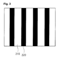
- the black matrix composition is coated on a front substrate of a plasma display panel 310 to form a black matrix 320.
- the black matrix 320 thus formed is shown in FIG. 3.
- an abnormal phenomenon of the black matrix 320 such as a cut off of the black matrix 320 or ununiformity of a width of the black matrix 320 is not generated.
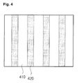
- a black matrix composition was provided in the same manner as in Example 1 except that 70 g of Co 3 O 4 was used as inorganic pigment and 70 g of Bi 2 O 3 -based glass powder was used as glass powder.
- the black matrix composition is coated on a front substrate of a plasma display panel 410 to form a black matrix 420.
- the black matrix 420 thus formed is shown in FIG. 4.
- an abnormal phenomenon of the black matrix 420 such as a cut off of the black matrix 420 or ununiformity of a width of the black matrix 420 is not generated.
- FIG. 5 shows a structure of a plasma display panel according to an embodiment of the present invention.
- the plasma display panel according to an embodiment of the present invention comprises a substrate 510, a black matrix 520 formed on the substrate 510 and an electrode layer 530 formed on the black matrix 520.
- a width of one surface of the black matrix 520 contacting with the substrate 510 is more than the width of the other surface of the black matrix 520 contacting with the electrode layer 530.
- the black matrix(520) is formed with a black matrix paste or a black matrix slurry, and the black matrix paste or the black matrix slurry comprises photo cross linkable organics comprising urethane acrylate oligomer, inorganic pigment and glass powder.
- the black matrix composition according to the present invention such as the black matrix paste or the black matrix slurry is the same as the above-described black matrix composition, a description thereof is omitted.
- the width of one surface of the black matrix 520 contacting with the substrate 510 is more than the width of the other surface of the black matrix 520 contacting with the electrode layer 530 by reason of an increase of an adhesiveness between the substrate 510 and the black matrix (520).
- a horizontal distance a between the edge E1 of the one surface and the edge E2 of the other surface is more than or equal to 0.1 ⁇ m to equal to or less than 10 ⁇ m.
- the horizontal distance a between the edge E1 of the one surface and the edge E2 of the other surface is more than or equal to 5 ⁇ m to equal to or less than 10 ⁇ m.
- the reference numeral 540 of FIG.5 is a DFR layer.
Landscapes
- Physics & Mathematics (AREA)
- Engineering & Computer Science (AREA)
- General Physics & Mathematics (AREA)
- Plasma & Fusion (AREA)
- Life Sciences & Earth Sciences (AREA)
- Environmental Sciences (AREA)
- Electromagnetism (AREA)
- Chemical & Material Sciences (AREA)
- Ceramic Engineering (AREA)
- Spectroscopy & Molecular Physics (AREA)
- Gas-Filled Discharge Tubes (AREA)
- Polymerisation Methods In General (AREA)
Applications Claiming Priority (2)
| Application Number | Priority Date | Filing Date | Title |
|---|---|---|---|
| KR1020050012938A KR20060091669A (ko) | 2005-02-16 | 2005-02-16 | 플라즈마 디스플레이 패널 전면기판용 블랙매트릭스 조성물 |
| EP06290263A EP1720232A3 (de) | 2005-02-16 | 2006-02-15 | Zusammensetzung für eine Schwarzmatrix für eine Plasmaanzeigetafel und Plasmaanzeigetafel |
Related Parent Applications (1)
| Application Number | Title | Priority Date | Filing Date |
|---|---|---|---|
| EP06290263A Division EP1720232A3 (de) | 2005-02-16 | 2006-02-15 | Zusammensetzung für eine Schwarzmatrix für eine Plasmaanzeigetafel und Plasmaanzeigetafel |
Publications (2)
| Publication Number | Publication Date |
|---|---|
| EP1850364A2 true EP1850364A2 (de) | 2007-10-31 |
| EP1850364A3 EP1850364A3 (de) | 2008-02-13 |
Family
ID=36579220
Family Applications (2)
| Application Number | Title | Priority Date | Filing Date |
|---|---|---|---|
| EP07109455A Withdrawn EP1850364A3 (de) | 2005-02-16 | 2006-02-15 | Plasmaanzeigetafel |
| EP06290263A Withdrawn EP1720232A3 (de) | 2005-02-16 | 2006-02-15 | Zusammensetzung für eine Schwarzmatrix für eine Plasmaanzeigetafel und Plasmaanzeigetafel |
Family Applications After (1)
| Application Number | Title | Priority Date | Filing Date |
|---|---|---|---|
| EP06290263A Withdrawn EP1720232A3 (de) | 2005-02-16 | 2006-02-15 | Zusammensetzung für eine Schwarzmatrix für eine Plasmaanzeigetafel und Plasmaanzeigetafel |
Country Status (5)
| Country | Link |
|---|---|
| US (1) | US20060181208A1 (de) |
| EP (2) | EP1850364A3 (de) |
| JP (1) | JP2006228736A (de) |
| KR (1) | KR20060091669A (de) |
| CN (1) | CN1831647A (de) |
Families Citing this family (9)
| Publication number | Priority date | Publication date | Assignee | Title |
|---|---|---|---|---|
| WO2007007800A1 (ja) * | 2005-07-13 | 2007-01-18 | Taiyo Ink Mfg. Co., Ltd. | 黒色ペースト組成物、及びそれを用いたブラックマトリックスパターンの形成方法、並びにそのブラックマトリックスパターン |
| US7615581B2 (en) | 2005-08-17 | 2009-11-10 | Lg Electronics Inc. | Black paste composite, upper plate of plasma display panel, and manufacturing method by using the same |
| TWI340755B (en) * | 2006-04-21 | 2011-04-21 | Hon Hai Prec Ind Co Ltd | Sensitive materials and manufacturing method for black matrix banks of ink jet color filter |
| KR100829704B1 (ko) * | 2007-06-04 | 2008-05-14 | 엘지전자 주식회사 | 플라즈마 디스플레이 패널 유전체용 조성물, 이를 포함하는플라즈마 디스플레이 패널 및 그 제조방법 |
| KR100905482B1 (ko) * | 2007-11-28 | 2009-07-02 | 엘지전자 주식회사 | 플라즈마 디스플레이 패널 유전체용 조성물, 이를 포함하는플라즈마 디스플레이 패널 |
| JP5601755B2 (ja) * | 2007-12-19 | 2014-10-08 | 太陽ホールディングス株式会社 | スラリー組成物 |
| JP2014205142A (ja) * | 2014-05-26 | 2014-10-30 | 太陽ホールディングス株式会社 | スラリー組成物 |
| KR102210938B1 (ko) | 2017-11-28 | 2021-02-01 | 주식회사 엘지화학 | 부착력이 우수한 도파관 엣지 차광용 조성물 |
| US11061294B1 (en) * | 2019-12-18 | 2021-07-13 | Tcl China Star Optoelectronics Technology Co., Ltd. | Black matrix composition, liquid crystal display panel and manufacturing method thereof |
Citations (2)
| Publication number | Priority date | Publication date | Assignee | Title |
|---|---|---|---|---|
| EP0740183A1 (de) | 1995-04-24 | 1996-10-30 | DAINICHI SEIKA COLOR & CHEMICALS MFG. CO. LTD. | Zusammensetzung für eine Schwarzmatrix, Herstellung einer Schwarzmatrix und Gegenstand mit einer solchen Matrix |
| EP1308982A2 (de) | 2001-11-05 | 2003-05-07 | Lg Electronics Inc. | Plasma-Anzeigetafel und Herstellungsverfahren davon |
Family Cites Families (9)
| Publication number | Priority date | Publication date | Assignee | Title |
|---|---|---|---|---|
| US6197480B1 (en) * | 1995-06-12 | 2001-03-06 | Toray Industries, Inc. | Photosensitive paste, a plasma display, and a method for the production thereof |
| JP3163563B2 (ja) * | 1995-08-25 | 2001-05-08 | 富士通株式会社 | 面放電型プラズマ・ディスプレイ・パネル及びその製造方法 |
| KR20000015469A (ko) * | 1998-08-29 | 2000-03-15 | 박이순 | 광중합형 감광성 형광체 페이스트 조성물및 이를 이용한 형광막의 형성방법 |
| KR100300422B1 (ko) * | 1999-02-25 | 2001-09-26 | 김순택 | 플라즈마 디스플레이 패널 |
| JP2001075086A (ja) * | 1999-07-05 | 2001-03-23 | Sharp Corp | 液晶表示装置及びその製造方法 |
| TW478007B (en) * | 1999-10-19 | 2002-03-01 | Matsushita Electric Industrial Co Ltd | Gas discharge panel and a manufacturing method for the same |
| US20030151362A1 (en) * | 2000-08-29 | 2003-08-14 | Gerald Alberto | Composition for the production of a black matrix, process for producing a black matrix and plasma display panel comprising such a black matrix |
| US7211950B2 (en) * | 2001-05-29 | 2007-05-01 | Choong Hoon Yi | Organic electro luminescent display and manufacturing method thereof |
| JP4431958B2 (ja) * | 2001-06-01 | 2010-03-17 | セイコーエプソン株式会社 | カラーフィルタ及び電気光学装置 |
-
2005
- 2005-02-16 KR KR1020050012938A patent/KR20060091669A/ko not_active Withdrawn
-
2006
- 2006-02-15 US US11/276,141 patent/US20060181208A1/en not_active Abandoned
- 2006-02-15 EP EP07109455A patent/EP1850364A3/de not_active Withdrawn
- 2006-02-15 EP EP06290263A patent/EP1720232A3/de not_active Withdrawn
- 2006-02-16 JP JP2006039615A patent/JP2006228736A/ja not_active Withdrawn
- 2006-02-16 CN CNA2006100088287A patent/CN1831647A/zh active Pending
Patent Citations (2)
| Publication number | Priority date | Publication date | Assignee | Title |
|---|---|---|---|---|
| EP0740183A1 (de) | 1995-04-24 | 1996-10-30 | DAINICHI SEIKA COLOR & CHEMICALS MFG. CO. LTD. | Zusammensetzung für eine Schwarzmatrix, Herstellung einer Schwarzmatrix und Gegenstand mit einer solchen Matrix |
| EP1308982A2 (de) | 2001-11-05 | 2003-05-07 | Lg Electronics Inc. | Plasma-Anzeigetafel und Herstellungsverfahren davon |
Also Published As
| Publication number | Publication date |
|---|---|
| KR20060091669A (ko) | 2006-08-21 |
| EP1850364A3 (de) | 2008-02-13 |
| EP1720232A2 (de) | 2006-11-08 |
| JP2006228736A (ja) | 2006-08-31 |
| EP1720232A3 (de) | 2007-03-21 |
| CN1831647A (zh) | 2006-09-13 |
| US20060181208A1 (en) | 2006-08-17 |
Similar Documents
| Publication | Publication Date | Title |
|---|---|---|
| KR100832654B1 (ko) | 페이스트, 디스플레이 부재 및 디스플레이 부재의 제조 방법 | |
| US6576391B1 (en) | Photosensitive paste a plasma display, and a method for the production thereof | |
| WO1999010909A1 (en) | Plasma display and method for manufacturing the same | |
| EP1850364A2 (de) | Plasmaanzeigetafel | |
| DE69607569T3 (de) | Benutzung einer fotoempfindlichen paste, verfahren zur herstellung einer plasmaanzeigetafel, sowie plasmaanzeigetafel, welche nach diesem verfahren herstellbar ist | |
| EP1967903B1 (de) | Lichtempfindliche pastöse Zusammensetzung, mit der Zusammensetzung hergestellte trennende Rippenstruktur und Plasmaanzeigetafel mit der trennenden Rippenstruktur | |
| JP3986312B2 (ja) | 黒色ペースト組成物及びそれを用いて黒色パターンを形成したプラズマディスプレイパネル | |
| KR100871075B1 (ko) | 인쇄용 페이스트 조성물 | |
| JP5209606B2 (ja) | 印刷用ペースト組成物 | |
| JP3538387B2 (ja) | 光硬化性樹脂組成物及びそれを用いて電極形成したプラズマディスプレイパネル | |
| JP3239759B2 (ja) | 感光性ペースト | |
| JP3548146B2 (ja) | 光硬化性組成物及びそれを用いて黒色パターンを形成したプラズマディスプレイパネル | |
| KR101404459B1 (ko) | 플라즈마 디스플레이 패널 격벽 형성용 감광성 페이스트조성물 및 플라즈마 디스플레이 패널 격벽 형성방법 | |
| CN101393393B (zh) | 等离子体显示屏电极形成用浆料组合物 | |
| JP2006310290A (ja) | ディスプレイ用前面板の製造方法およびそれを用いたプラズマディスプレイ | |
| JP4771598B2 (ja) | 光硬化性樹脂組成物及びそれを用いてブラックマトリックスを形成したプラズマディスプレイパネル | |
| US6372292B1 (en) | Insulating paste composition for rib formation and method of rib pattern formulation | |
| JP2004148585A (ja) | エレメントおよびその利用 | |
| JP2002025431A (ja) | 障壁形成用樹脂組成物エレメント及びこれを用いたプラズマディスプレイパネル用基板の製造法 | |
| KR101097429B1 (ko) | Pdp 전극의 흑색층 형성용 조성물 | |
| JP2002025432A (ja) | 誘電体層及び障壁形成用樹脂組成物エレメント及びこれを用いたプラズマディスプレイパネル用基板の製造法 | |
| JP3858005B2 (ja) | 光硬化性樹脂組成物及びプラズマディスプレイパネル用前面基板 | |
| JPH10144213A (ja) | 感光性ガラスペースト組成物 | |
| JP2002025429A (ja) | プラズマディスプレイパネル用基板の製造法 | |
| JP2002008525A (ja) | 誘電体層及び障壁形成用樹脂組成物エレメント及びこれを用いたプラズマディスプレイパネル用基板の製造法 |
Legal Events
| Date | Code | Title | Description |
|---|---|---|---|
| PUAI | Public reference made under article 153(3) epc to a published international application that has entered the european phase |
Free format text: ORIGINAL CODE: 0009012 |
|
| AC | Divisional application: reference to earlier application |
Ref document number: 1720232 Country of ref document: EP Kind code of ref document: P |
|
| AK | Designated contracting states |
Kind code of ref document: A2 Designated state(s): AT BE BG CH CY CZ DE DK EE ES FI FR GB GR HU IE IS IT LI LT LU LV MC NL PL PT RO SE SI SK TR |
|
| AX | Request for extension of the european patent |
Extension state: AL BA HR MK YU |
|
| PUAL | Search report despatched |
Free format text: ORIGINAL CODE: 0009013 |
|
| AK | Designated contracting states |
Kind code of ref document: A3 Designated state(s): AT BE BG CH CY CZ DE DK EE ES FI FR GB GR HU IE IS IT LI LT LU LV MC NL PL PT RO SE SI SK TR |
|
| AX | Request for extension of the european patent |
Extension state: AL BA HR MK YU |
|
| 17P | Request for examination filed |
Effective date: 20080813 |
|
| AKX | Designation fees paid |
Designated state(s): DE FR GB NL |
|
| STAA | Information on the status of an ep patent application or granted ep patent |
Free format text: STATUS: THE APPLICATION IS DEEMED TO BE WITHDRAWN |
|
| 18D | Application deemed to be withdrawn |
Effective date: 20100901 |