EP1850383A1 - Diode électroluminescente à trois longueurs d'onde - Google Patents
Diode électroluminescente à trois longueurs d'onde Download PDFInfo
- Publication number
- EP1850383A1 EP1850383A1 EP06008505A EP06008505A EP1850383A1 EP 1850383 A1 EP1850383 A1 EP 1850383A1 EP 06008505 A EP06008505 A EP 06008505A EP 06008505 A EP06008505 A EP 06008505A EP 1850383 A1 EP1850383 A1 EP 1850383A1
- Authority
- EP
- European Patent Office
- Prior art keywords
- led chip
- wavelength
- emitting diode
- led
- light led
- Prior art date
- Legal status (The legal status is an assumption and is not a legal conclusion. Google has not performed a legal analysis and makes no representation as to the accuracy of the status listed.)
- Withdrawn
Links
Images


Classifications
-
- H—ELECTRICITY
- H10—SEMICONDUCTOR DEVICES; ELECTRIC SOLID-STATE DEVICES NOT OTHERWISE PROVIDED FOR
- H10W—GENERIC PACKAGES, INTERCONNECTIONS, CONNECTORS OR OTHER CONSTRUCTIONAL DETAILS OF DEVICES COVERED BY CLASS H10
- H10W90/00—Package configurations
-
- H—ELECTRICITY
- H10—SEMICONDUCTOR DEVICES; ELECTRIC SOLID-STATE DEVICES NOT OTHERWISE PROVIDED FOR
- H10H—INORGANIC LIGHT-EMITTING SEMICONDUCTOR DEVICES HAVING POTENTIAL BARRIERS
- H10H20/00—Individual inorganic light-emitting semiconductor devices having potential barriers, e.g. light-emitting diodes [LED]
- H10H20/80—Constructional details
- H10H20/85—Packages
- H10H20/851—Wavelength conversion means
-
- H—ELECTRICITY
- H10—SEMICONDUCTOR DEVICES; ELECTRIC SOLID-STATE DEVICES NOT OTHERWISE PROVIDED FOR
- H10W—GENERIC PACKAGES, INTERCONNECTIONS, CONNECTORS OR OTHER CONSTRUCTIONAL DETAILS OF DEVICES COVERED BY CLASS H10
- H10W72/00—Interconnections or connectors in packages
- H10W72/01—Manufacture or treatment
- H10W72/015—Manufacture or treatment of bond wires
- H10W72/01515—Forming coatings
-
- H—ELECTRICITY
- H10—SEMICONDUCTOR DEVICES; ELECTRIC SOLID-STATE DEVICES NOT OTHERWISE PROVIDED FOR
- H10W—GENERIC PACKAGES, INTERCONNECTIONS, CONNECTORS OR OTHER CONSTRUCTIONAL DETAILS OF DEVICES COVERED BY CLASS H10
- H10W72/00—Interconnections or connectors in packages
- H10W72/071—Connecting or disconnecting
- H10W72/075—Connecting or disconnecting of bond wires
-
- H—ELECTRICITY
- H10—SEMICONDUCTOR DEVICES; ELECTRIC SOLID-STATE DEVICES NOT OTHERWISE PROVIDED FOR
- H10W—GENERIC PACKAGES, INTERCONNECTIONS, CONNECTORS OR OTHER CONSTRUCTIONAL DETAILS OF DEVICES COVERED BY CLASS H10
- H10W72/00—Interconnections or connectors in packages
- H10W72/50—Bond wires
- H10W72/541—Dispositions of bond wires
- H10W72/547—Dispositions of multiple bond wires
- H10W72/5473—Dispositions of multiple bond wires multiple bond wires connected to a common bond pad
-
- H—ELECTRICITY
- H10—SEMICONDUCTOR DEVICES; ELECTRIC SOLID-STATE DEVICES NOT OTHERWISE PROVIDED FOR
- H10W—GENERIC PACKAGES, INTERCONNECTIONS, CONNECTORS OR OTHER CONSTRUCTIONAL DETAILS OF DEVICES COVERED BY CLASS H10
- H10W74/00—Encapsulations, e.g. protective coatings
-
- H—ELECTRICITY
- H10—SEMICONDUCTOR DEVICES; ELECTRIC SOLID-STATE DEVICES NOT OTHERWISE PROVIDED FOR
- H10W—GENERIC PACKAGES, INTERCONNECTIONS, CONNECTORS OR OTHER CONSTRUCTIONAL DETAILS OF DEVICES COVERED BY CLASS H10
- H10W90/00—Package configurations
- H10W90/701—Package configurations characterised by the relative positions of pads or connectors relative to package parts
- H10W90/751—Package configurations characterised by the relative positions of pads or connectors relative to package parts of bond wires
- H10W90/756—Package configurations characterised by the relative positions of pads or connectors relative to package parts of bond wires between a chip and a stacked lead frame, conducting package substrate or heat sink
Definitions
- the present invention relates to LED field, and more particularly to a three wavelength LED structure.
- LED Light emitting diode
- Fig. 1 is a conventional bulb-shaped single color LED package structure.
- a single color LED chip 11 is placed in a cup 101 of an electrode supporting frame 10 and is electrically connected to another electrode supporting frame 13 by a wire 12.
- the cup 101 is filled with a transparent resin 14 for sealing and protecting the single color LED chip 11, and finally, these components are encapsulated by a colloid 15, thus forming a bulb type single color LED.
- this conventional single color LED uses the chip as a light source, it only can generate a single color light due to the physical characteristic of the LED. If want to generate multiple colored light, it requires the cooperation of multicolor chips. However, according to the color forming principle, the cooperation of three primary color LED chips (red, blue and green) is unable to produce an even white light, therefore, the applicability of the LED chip is limited.
- the resin contains chemical substances that can switch wavelength, so that the substances in the resin can convert light color by color mixing or absorbing. Therefore, the LED can be used as a multicolor light source.
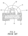
- Fig. 2 which shows a white light LED package structure formed by surface mounting technology.
- conductive layers 17 and 18 are arranged on the periphery of a substrate 16.
- a blue light LED chip 19 is placed on the conductive layer 17 and is electrically connected to the conductive layers 17 and 18, respectively, by two welding wires 20 and 21.
- the blue light LED chip 19 is coated with a resin 22 containing yellow fluorescent agents, and then is encapsulated by a colloid 23, thus forming a white light LED package structure.
- the white light LED package structure shown in Fig. 2 uses the blue light LED chip as a light source, and the resin having yellow fluorescent agent converts the blue light into white light. Therefore, this white light LED package structure can be used as a white light source, and because its primary color is blue, a part of the blue light will leak through the clearance of the fluorescent layer, creating an effect that the white light looks very clean and clear.
- the light generated by the conventional LED is white only in visual effect, but in fact, the white light is a combination of blue light and yellow light, without the red light, and the light color cannot be changed once the final product is finished.
- the color temperature of the conventional white light LED is difficult to control, and particularly, it is unable to produce a warm effect at the color temperature of 3500k.
- the color rendering of the produced white light is very poor, it is unable to completely replace the white light source.
- the present invention has arisen to mitigate and/or obviate the afore-described disadvantages.
- the primary objective of the present invention is to provide a three wavelength LED structure that can generate white lights of different color temperatures.
- the secondary objective of the present invention is to provide a three wavelength LED structure that can generate neutral color light.
- Another objective of the present invention is to provide a three wavelength LED structure whose light color is adjustable within a limited range.
- a three wavelength LED structure provided in accordance with the present invention comprise a substrate, a conductive structure on the substrate, at least one blue light LED chip, at least one green light LED chip and a red fluorescent layer.
- the blue light LED chip and the green light LED chip are placed on the substrate or on the conductive structure and electrically connected to the conductive structure.
- the blue light LED chip does not contact the green light LED chip.
- the blue light LED chip and the green light LED chip are encapsulated by the red fluorescent layer and the red fluorescent layer can covert the wavelength emitted by the two LED chips.
- the blue light LED chip and the green light LED chip are used as light sources, and a red fluorescent layer is used as a light transition medium.
- a red fluorescent layer is used as a light transition medium.
- the three wavelength LED structure of the present invention uses the blue light LED chip and the green light LED chip as light sources, and a red fluorescent layer is used as a light transition layer.
- the increase and decrease in operation current can cause a shift of CIE coordinate of the two LED chips, and the red fluorescent layer can convert the light emitted from the two LED chips into neutral color light, thus achieving the objective of providing neutral color light.
- the three wavelength LED structure of the present invention can produce a shift of CIE coordinate that changes with time, thus light color of the three wavelength LED is adjustable within a limited range.
- a three wavelength LED structure in accordance with an embodiment of the present invention is illustrated, wherein the three wavelength LED structure is used in a bulb type LED package structure.
- a blue LED chip 25 having a wavelength of 420-475 nm and a green LED chip 26 having a wavelength of 495-550 nm are placed in a cup 241 formed at the end of a electrode supporting frame 24, and the two LED chips 25 and 26 are electrically connected to another electrode supporting frame 29 by welding wires 27 and 28.
- a red fluorescent layer 30 is filled in the cup 241 and coated on the two LED chips 25 and 26.
- the red fluorescent layer 30 is made of composite colloid (such as: epoxy resin or silicone rubber) consisted of CaS:Eu 2+ ,or SrS:Eu 2+ , or the Europium activated Nitridosilicates Ca 2 Si 5 N 7 :Eu, Ca 2 Si 5 N 8 :Eu 2+ .
- the red fluorescent layer 30 can absorb one of the wavelengths of the two LED chips 25 and 26.
- CaS:Eu 2+ can absorb the light of wavelength 420-570 nm and generate a red spectrum of wavelength 655 nm.
- SrS:Eu 2+ can absorb the light of wavelength of 400-530 nm and generate a red spectrum of wavelength 625 nm.
- Europium activated Nitridosilicates can absorb the light of wavelength of 300-550 nm and generate a red spectrum of wavelength 600-700 nm.
- these components are encapsulated by a colloid 31, thus forming a bulb-type LED package structure.
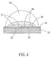
- FIG. 4 shows another embodiment of the present invention, wherein the three wavelength LED structure is applied to a surface mounting type LED package structure.
- a blue LED chip 25 having a wavelength of 420-475 nm and a green LED chip 26 having a wavelength of 495-550 nm are placed on a printed circuit layer 33, and the printed circuit layer 33 is located on a substrate 32.
- the LED chips 25 and 26 are electrically connected to the printed circuit layer 33, respectively, by two welding wires 27 and 28.
- the red fluorescent layer 30 is filled in the cup 241 and coated on the two LED chips 25 and 26.
- the red fluorescent layer 30 is made of composite colloid (such as: epoxy resin or silicone rubber) consisted of CaS:Eu 2+ ,orSrS:Eu 2+ ,or the Europium activated Nitridosilicates Ca 2 Si 5 N 7 :Eu, Ca 2 Si 5 N 8 :Eu 2+ .
- the red fluorescent layer 30 can absorb one of the wavelengths of the two LED chips 25 and 26.
- CaS:Eu 2+ can absorb the light of wavelength 420-570 nm and generate a red spectrum of peak wavelength 655 nm.
- SrS:Eu 2+ can absorb the light of wavelength of 400-530 nm and generate a red spectrum of peak wavelength 625 nm.
- Europium activated Nitridosilicates can absorb the light of wavelength of 300-550 nm and generate a red spectrum of wavelength 600-700 nm.
- these components are encapsulated by a transparent colloid 34, thus forming a surface mounting type LED package structure.
- the abovementioned three wavelength LED structure utilizes the chemical substances of the red fluorescent layer to absorb the blue and green lights generated from the blue and green LED chips. After absorbing the blue and green lights, the chemical substances can generate red spectrum of wavelength 600-700 nm, and the red spectrum will be mixed with the blue and green lights to form a white light (the three primary colors forming white light is red, green and blue).
- the blue LED chip and the green LED chip are the same in electrical property, and they are generally the same in forward voltage and current, accordingly, it can use a drive circuit to control the blue LED chip and the green LED chip.
- it can adjust the number of the blue and the green LED chips in the three wavelength LED structure.
- the proportion between the blue and green LED chips can be 1:3, 1:2, 1:1, 2:1, 3:1, etc, and with the adjustment in the amount of the chemical substances, the color temperature can be adjusted between 2500K-7000K.
- the white light generated by this structure is consisted of three primary colors (red, green and blue), and its color rendering index (Ra) will be as high as 90, thus improving the practical value of the present invention.
- the increase and decrease in operation current will lead to a shift of CIE coordinate.
- the dosage of the chemical substances in the red fluorescent agent when producing the LED package structure the light mixed by the blue light, the green light and the light generated after the activation of the chemical substances will be slightly reddish, greenish or bluish, thus creating different neutral colors, such as pink, baby blue, light green, light yellow or milky white.
- the value of the drive current of the blue LED chip and that of the green LED chip are adjusted in time sequence, the CIE coordinate will shift with time. By taking the use of the phenomenon of CIE coordinate shift, it can produce a LED that is adjustable in light color.
- the advantage is that even if the three wavelength LED of the present invention has been processed into a finished product, the finished product of the LED still can generate different-colored lights by using different circuits to control the blue and the green LED chips or by using the design of time sequence control, thus improving the practical value of the present invention.
- the three wavelength LED structure of the present invention uses the blue light LED chip and the green light LED chip as light sources, and a red fluorescent layer is used as a light transition layer.
- a white light LED which is adjustable in color temperature, a neutral color LED whose color is changeable, or can produce a LED whose light color changes with time.
Landscapes
- Led Device Packages (AREA)
- Led Devices (AREA)
Priority Applications (1)
| Application Number | Priority Date | Filing Date | Title |
|---|---|---|---|
| EP06008505A EP1850383A1 (fr) | 2006-04-25 | 2006-04-25 | Diode électroluminescente à trois longueurs d'onde |
Applications Claiming Priority (1)
| Application Number | Priority Date | Filing Date | Title |
|---|---|---|---|
| EP06008505A EP1850383A1 (fr) | 2006-04-25 | 2006-04-25 | Diode électroluminescente à trois longueurs d'onde |
Publications (1)
| Publication Number | Publication Date |
|---|---|
| EP1850383A1 true EP1850383A1 (fr) | 2007-10-31 |
Family
ID=37036960
Family Applications (1)
| Application Number | Title | Priority Date | Filing Date |
|---|---|---|---|
| EP06008505A Withdrawn EP1850383A1 (fr) | 2006-04-25 | 2006-04-25 | Diode électroluminescente à trois longueurs d'onde |
Country Status (1)
| Country | Link |
|---|---|
| EP (1) | EP1850383A1 (fr) |
Cited By (9)
| Publication number | Priority date | Publication date | Assignee | Title |
|---|---|---|---|---|
| WO2009157999A1 (fr) * | 2008-06-25 | 2009-12-30 | Cree, Inc. | Appareils d'éclairage à semi-conducteurs comprenant des mélanges de lumière |
| US7821194B2 (en) | 2006-04-18 | 2010-10-26 | Cree, Inc. | Solid state lighting devices including light mixtures |
| US7967652B2 (en) | 2009-02-19 | 2011-06-28 | Cree, Inc. | Methods for combining light emitting devices in a package and packages including combined light emitting devices |
| US8333631B2 (en) | 2009-02-19 | 2012-12-18 | Cree, Inc. | Methods for combining light emitting devices in a package and packages including combined light emitting devices |
| US8556469B2 (en) | 2010-12-06 | 2013-10-15 | Cree, Inc. | High efficiency total internal reflection optic for solid state lighting luminaires |
| US8684559B2 (en) | 2010-06-04 | 2014-04-01 | Cree, Inc. | Solid state light source emitting warm light with high CRI |
| US8998444B2 (en) | 2006-04-18 | 2015-04-07 | Cree, Inc. | Solid state lighting devices including light mixtures |
| US9435493B2 (en) | 2009-10-27 | 2016-09-06 | Cree, Inc. | Hybrid reflector system for lighting device |
| JP2019114637A (ja) * | 2017-12-22 | 2019-07-11 | 日亜化学工業株式会社 | 発光装置 |
Citations (9)
| Publication number | Priority date | Publication date | Assignee | Title |
|---|---|---|---|---|
| EP1160883A2 (fr) * | 2000-05-31 | 2001-12-05 | Matsushita Electric Industrial Co., Ltd. | Lampe à diode électroluminescente |
| US20030227022A1 (en) * | 2002-06-06 | 2003-12-11 | Hwang Chin-Mau James | White light source |
| DE10233050A1 (de) * | 2002-07-19 | 2004-02-05 | Osram Opto Semiconductors Gmbh | Lichtquelle auf LED-Basis, insbesondere für die Erzeugung von weißem Licht |
| US20040207313A1 (en) * | 2003-04-21 | 2004-10-21 | Sharp Kabushiki Kaisha | LED device and portable telephone, digital camera and LCD apparatus using the same |
| WO2004100275A1 (fr) * | 2003-05-01 | 2004-11-18 | Cree, Inc. | Lampe emettrice de lumiere blanche |
| US20050117334A1 (en) * | 2003-11-27 | 2005-06-02 | Kun-Chui Lee | Light emitting device |
| WO2005109532A1 (fr) * | 2004-05-06 | 2005-11-17 | Seoul Opto-Device Co., Ltd. | Dispositif luminescent |
| WO2005112137A1 (fr) * | 2004-05-13 | 2005-11-24 | Seoul Opto-Device Co., Ltd. | Dispositif electroluminescent comprenant des diodes electroluminescentes rouge verte bleue et du phosphore |
| DE102005020695A1 (de) * | 2004-04-30 | 2005-12-15 | Optotransmitter-Umweltschutz-Technologie E.V. | Vorrichtung zur Emission von Strahlung mit einstellbarer Spektraleigenschaft |
-
2006
- 2006-04-25 EP EP06008505A patent/EP1850383A1/fr not_active Withdrawn
Patent Citations (9)
| Publication number | Priority date | Publication date | Assignee | Title |
|---|---|---|---|---|
| EP1160883A2 (fr) * | 2000-05-31 | 2001-12-05 | Matsushita Electric Industrial Co., Ltd. | Lampe à diode électroluminescente |
| US20030227022A1 (en) * | 2002-06-06 | 2003-12-11 | Hwang Chin-Mau James | White light source |
| DE10233050A1 (de) * | 2002-07-19 | 2004-02-05 | Osram Opto Semiconductors Gmbh | Lichtquelle auf LED-Basis, insbesondere für die Erzeugung von weißem Licht |
| US20040207313A1 (en) * | 2003-04-21 | 2004-10-21 | Sharp Kabushiki Kaisha | LED device and portable telephone, digital camera and LCD apparatus using the same |
| WO2004100275A1 (fr) * | 2003-05-01 | 2004-11-18 | Cree, Inc. | Lampe emettrice de lumiere blanche |
| US20050117334A1 (en) * | 2003-11-27 | 2005-06-02 | Kun-Chui Lee | Light emitting device |
| DE102005020695A1 (de) * | 2004-04-30 | 2005-12-15 | Optotransmitter-Umweltschutz-Technologie E.V. | Vorrichtung zur Emission von Strahlung mit einstellbarer Spektraleigenschaft |
| WO2005109532A1 (fr) * | 2004-05-06 | 2005-11-17 | Seoul Opto-Device Co., Ltd. | Dispositif luminescent |
| WO2005112137A1 (fr) * | 2004-05-13 | 2005-11-24 | Seoul Opto-Device Co., Ltd. | Dispositif electroluminescent comprenant des diodes electroluminescentes rouge verte bleue et du phosphore |
Cited By (12)
| Publication number | Priority date | Publication date | Assignee | Title |
|---|---|---|---|---|
| US7821194B2 (en) | 2006-04-18 | 2010-10-26 | Cree, Inc. | Solid state lighting devices including light mixtures |
| US8212466B2 (en) | 2006-04-18 | 2012-07-03 | Cree, Inc. | Solid state lighting devices including light mixtures |
| US8998444B2 (en) | 2006-04-18 | 2015-04-07 | Cree, Inc. | Solid state lighting devices including light mixtures |
| WO2009157999A1 (fr) * | 2008-06-25 | 2009-12-30 | Cree, Inc. | Appareils d'éclairage à semi-conducteurs comprenant des mélanges de lumière |
| CN102124263B (zh) * | 2008-06-25 | 2013-07-24 | 克里公司 | 包括光混合的固态照明装置 |
| US7967652B2 (en) | 2009-02-19 | 2011-06-28 | Cree, Inc. | Methods for combining light emitting devices in a package and packages including combined light emitting devices |
| US8333631B2 (en) | 2009-02-19 | 2012-12-18 | Cree, Inc. | Methods for combining light emitting devices in a package and packages including combined light emitting devices |
| US9435493B2 (en) | 2009-10-27 | 2016-09-06 | Cree, Inc. | Hybrid reflector system for lighting device |
| US8684559B2 (en) | 2010-06-04 | 2014-04-01 | Cree, Inc. | Solid state light source emitting warm light with high CRI |
| US9599291B2 (en) | 2010-06-04 | 2017-03-21 | Cree, Inc. | Solid state light source emitting warm light with high CRI |
| US8556469B2 (en) | 2010-12-06 | 2013-10-15 | Cree, Inc. | High efficiency total internal reflection optic for solid state lighting luminaires |
| JP2019114637A (ja) * | 2017-12-22 | 2019-07-11 | 日亜化学工業株式会社 | 発光装置 |
Similar Documents
| Publication | Publication Date | Title |
|---|---|---|
| US20070108455A1 (en) | Three wavelength LED structure | |
| EP2671019B1 (fr) | Appareil d'éclairage produisant un flux lumineux accru tout en maintenant le point de couleur et le cri | |
| US11817531B1 (en) | Phosphor-converted red LEDs and color-tunable multi-LED lighting devices | |
| US7781783B2 (en) | White light LED device | |
| US9231170B2 (en) | Phosphor LED | |
| JP2019534541A (ja) | 連続スペクトルを有するチューナブルled発光体 | |
| JP2017059854A (ja) | 高演色性白色発光素子 | |
| CN102057509B (zh) | 具有多波段磷光体体系的led | |
| US7834372B2 (en) | High luminous flux warm white solid state lighting device | |
| JP2011216868A (ja) | 発光装置及び照明装置 | |
| JP2021168416A (ja) | 発光装置および調色装置 | |
| JP2013537714A (ja) | 離隔蛍光体構成で成形/形成及び使用される、シリコーン中に懸濁した蛍光体 | |
| US20200053852A1 (en) | Light emitting device | |
| EP2830093A1 (fr) | Module à DEL comprenant un indice de rendu de couleur élevé | |
| KR100612962B1 (ko) | 삼파장 형광체를 이용한 백색 발광 다이오드 | |
| KR20110034207A (ko) | 발광다이오드 패키지 및 이의 제조방법 | |
| JP2022055685A (ja) | 多色led光源装置 | |
| JP2010212621A (ja) | 発光装置 | |
| CN1971908A (zh) | 三波长led结构 | |
| JP2010177368A (ja) | Led装置の製造方法 | |
| CN101261981A (zh) | 暖色系光源 | |
| KR101855391B1 (ko) | 고연색성 백색 발광 소자 | |
| WO2023134217A1 (fr) | Del rouges converties au luminophore et dispositifs électroluminescents emballés à del multiples accordables en couleur | |
| EP4599186A1 (fr) | Dispositif en forme de filament électroluminescent | |
| CN118866889A (zh) | 一种多色多功能led器件及其照明装置 |
Legal Events
| Date | Code | Title | Description |
|---|---|---|---|
| PUAI | Public reference made under article 153(3) epc to a published international application that has entered the european phase |
Free format text: ORIGINAL CODE: 0009012 |
|
| AK | Designated contracting states |
Kind code of ref document: A1 Designated state(s): AT BE BG CH CY CZ DE DK EE ES FI FR GB GR HU IE IS IT LI LT LU LV MC NL PL PT RO SE SI SK TR |
|
| AX | Request for extension of the european patent |
Extension state: AL BA HR MK YU |
|
| AKX | Designation fees paid | ||
| STAA | Information on the status of an ep patent application or granted ep patent |
Free format text: STATUS: THE APPLICATION IS DEEMED TO BE WITHDRAWN |
|
| 18D | Application deemed to be withdrawn |
Effective date: 20080503 |
|
| REG | Reference to a national code |
Ref country code: DE Ref legal event code: 8566 |