EP1850390A2 - Module de dispositif d'affichage - Google Patents
Module de dispositif d'affichage Download PDFInfo
- Publication number
- EP1850390A2 EP1850390A2 EP06020940A EP06020940A EP1850390A2 EP 1850390 A2 EP1850390 A2 EP 1850390A2 EP 06020940 A EP06020940 A EP 06020940A EP 06020940 A EP06020940 A EP 06020940A EP 1850390 A2 EP1850390 A2 EP 1850390A2
- Authority
- EP
- European Patent Office
- Prior art keywords
- display device
- line
- device module
- lines
- electrode
- Prior art date
- Legal status (The legal status is an assumption and is not a legal conclusion. Google has not performed a legal analysis and makes no representation as to the accuracy of the status listed.)
- Withdrawn
Links
Images


Classifications
-
- H—ELECTRICITY
- H10—SEMICONDUCTOR DEVICES; ELECTRIC SOLID-STATE DEVICES NOT OTHERWISE PROVIDED FOR
- H10K—ORGANIC ELECTRIC SOLID-STATE DEVICES
- H10K59/00—Integrated devices, or assemblies of multiple devices, comprising at least one organic light-emitting element covered by group H10K50/00
- H10K59/10—OLED displays
- H10K59/12—Active-matrix OLED [AMOLED] displays
- H10K59/131—Interconnections, e.g. wiring lines or terminals
-
- H—ELECTRICITY
- H05—ELECTRIC TECHNIQUES NOT OTHERWISE PROVIDED FOR
- H05B—ELECTRIC HEATING; ELECTRIC LIGHT SOURCES NOT OTHERWISE PROVIDED FOR; CIRCUIT ARRANGEMENTS FOR ELECTRIC LIGHT SOURCES, IN GENERAL
- H05B33/00—Electroluminescent light sources
- H05B33/12—Light sources with substantially two-dimensional [2D] radiating surfaces
- H05B33/26—Light sources with substantially two-dimensional [2D] radiating surfaces characterised by the composition or arrangement of the conductive material used as an electrode
-
- H—ELECTRICITY
- H10—SEMICONDUCTOR DEVICES; ELECTRIC SOLID-STATE DEVICES NOT OTHERWISE PROVIDED FOR
- H10K—ORGANIC ELECTRIC SOLID-STATE DEVICES
- H10K59/00—Integrated devices, or assemblies of multiple devices, comprising at least one organic light-emitting element covered by group H10K50/00
- H10K59/10—OLED displays
- H10K59/17—Passive-matrix OLED displays
- H10K59/179—Interconnections, e.g. wiring lines or terminals
Definitions
- the present invention relates to a display device module, particularly relates to a display device module in which metal wires are effectively arranged on the substrate and contacted easily with an pin or jig.
- Fig. 1 is a plane view of the conventional organic electroluminescent device comprising a pixel circuit section, the conventional organic electroluminescent device from which a cap is removed is illustrated in Fig. 1 for convenience' sake.
- the pixel circuit section AA comprises anode electrodes formed on the substrate, an organic electroluminescent light emitting layer formed on the anode electrodes and cathode electrodes formed on the organic electroluminescent light emitting layer.
- Data lines 2A and scan lines 4A formed on the mother substrate are electrically connected to the anode electrodes and the cathode electrodes (not show) formed in the pixel circuit section AA, respectively, and end portions of the data lines 2A and the scan lines 4A are concentrated on a portion of the mother substrate 1 to form a pad P .
- the reference numerals " 4A-1 " and “ 2A-1 " which are not illustrated indicate connecting bars (so called as “short bar") formed ends of the scan lines 4A and the data lines 2A, a plurality of scan lines 4A and a plurality of data lines 2A are connected to each other by the connecting bars 4A-1 and 2A-1 .
- the reference numeral " S " indicates a region on which the cap will be bonded.
- the COG (chip on glass) type display device module has been used, in the COG type display device module, a film on which the device-driving unit (IC chip) is mounted is not used for connecting the organic electroluminescent device (hereinafter, referred to as "panel") shown in Fig. 1 and the device-driving unit, the device-driving unit is directly mounted on the substrate on which the pixel circuit section is formed
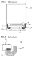
- Fig. 2 is a plane view of the COG type organic electroluminescent device module, Fig. 2 shows that a device-driving unit 11 is mounted on a substrate 10.
- the data lines 12 connected electrically the pixel circuit section can be connected directly to the device-driving unit 11.
- the scan lines 14 arranged on both sides of the data lines 12 are gone through the both sides of the device-driving unit 11 and then connected to a portion opposite to the portion corresponding to the pixel circuit section 13.
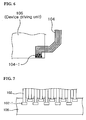
- Fig. 3 and Fig. 4 are enlarged views of " A " section of Fig. 2 and show a relation between the scan line 14 ( 14-1 ) and the device-driving unit 11 in the COG type organic electroluminescent device module.
- Fig. 3 and Fig. 4 show only a portion of the device-driving unit 11 and a portion of the scan lines 14, 14-1. Also, the device-driving unit 11 is shown in a transparent state so as to illustrate an arrangement of the scan lines 14 and 14-1.
- the scan lines 14 gone through the sides of the device-driving unit 11 and connected to a portion of the device-driving unit 11 opposite to the portion corresponding to the pixel circuit section ( 13 in Fig. 2) do not have a connecting bar.
- an end of respective scan line 14 is connected to a connecting terminal 11-1 (hereinafter, referred to as "bump") formed on the device-driving unit 11 (a state of Fig. 3).
- the scan lines 14-1 have a connecting bar 14A-1 formed at ends thereof, a portion of each scan line 14-1 is connected to the bump 11-1 of the device-driving unit 11 (a state of Fig. 4).
- a scratch can be formed on the scan line 14 or the scan line 14 can be peeled from the substrate 10 (so called as "a peeling phenomenon).
- the lighting inspection or the aging process is carried out after mounting the device-driving unit 11 on the substrate 10.
- the panel is inferior, the expensive device-driving unit 11 should be scrapped along with the panel.
- the connecting bar 14A-1 formed on the substrate 10 should be separated from the scan lines 14-1 prior to mounting the device-driving unit 11.
- a laser scribing process is additionally performed to cut the scan lines 14-1 along a scribe line L1.
- the present invention is conceived to solve the above problems generated in the display device module in which the device-driving unit is mounted on the substrate, an object of the present invention is to provide the display device module in which the first and second lines can be connected easily to a device-driving unit or a connecting means on which the device-driving unit is mounted.
- Another object of the present invention is to provide the display device module which can prevent the first and second lines from being damaged by contact between the line and a test pin or jig.
- a display device module comprises a pixel circuit section including at least one light emitting area, each light emitting area being formed at an overlying area of a substrate between a first electrode and a second electrode on a substrate; at least one first line being electrically connected to the first electrode in the pixel circuit section; at least one second line being electrically connected to the second electrode in the pixel circuit section, wherein each of the first lines and the second lines has a connecting portion formed thereon and the connecting portion is larger than the line in the width.
- the connecting portions are alternated with the connecting portion(s) of the neighbor line(s) so as to prevent two adjacent connecting portions from being contacted with each other.
- the display device module according to the present invention further comprises an insulating layer formed on a portion of the substrate including a connecting portion of each line, the insulating layer has openings formed thereon corresponding to the connecting portions.
- the connecting portion has a plane surface which is on the same level with that of the insulating layer, and the connecting portion is formed such that a portion of the connecting portion is protruded from the insulating layer through the opening.
- the display device module comprises a device driving unit mounted on the substrate area and being electrically connected to the first and second lines through the connecting portions.
- the display device module according to the present invention further comprises a connecting means mounted on the substrate and being electrically connected to the first and second lines to a device driving unit installed outside of the substrate, the connecting means is a film on which the device driving unit is mounted.
- Fig. 1 is a plane view of the conventional organic electroluminescent device on which a cap is not bonded;
- Fig. 2 is a plane view of the COG type organic electroluminescent device module
- Fig. 3 and Fig. 4 are enlarged views of "A" section of Fig. 2 and show an arrangement of the scan lines in the COG type organic electroluminescent device module;
- Fig. 5 is a plane view of the COG type organic electroluminescent device module according to the present invention.
- Fig. 6 is a view showing an arrangement of the scan lines on a device driving unit-mounting area of a substrate.
- Fig. 7 is a view showing an arrangement of the data lines on a device driving unit-mounting are of a substrate.
- the organic electroluminescent device is provided as an example of the light emitting device. It is, however, obvious that the teaching of the present invention is not limited to the organic electroluminescent device.
- the organic electroluminescent device (hereinafter, referred to as "panel") comprises at least one light emitting area formed by at least one anode electrode ("first electrode”) formed on the substrate, an organic electroluminescent light emitting layer formed on the anode electrodes and at least one cathode electrode (“second electrode”)formed on the organic electroluminescent light emitting layer.
- first electrode anode electrode
- second electrode cathode electrode
- an order for forming the cathode electrodes and the anode electrodes can be opposed to that for forming the above structure.
- the substrate on which the above elements are provided can be made of the various material including conductive material and nonconductive material such as plastic film, silicon, glass and the like.
- the conductive material can act as transistor in the active type organic electroluminescent device.
- Fig. 5 is a plane view of the COG type organic electroluminescent device module according to the present invention, Fig. 5 shows data lines ("first lines”) 102 , scan lines ("second lines”) 104 and a pixel circuit section including the anode electrodes, the organic electroluminescent light emitting layer and the anode electrodes.
- the pixel circuit section is not shown by a cap.
- the reference numeral " 120 " indicates the pixel circuit section.
- the reference numeral " 110 " in Fig. 5 indicated the “panel” on which the device-driving unit is not mounted, and the reference numeral “ L1 " is a scribed line along the module is individualized.
- a specific area 106 is provided on a region adjacent to the pixel circuit section 120, a device-driving unit (or a connecting means) is mounted on the area 106 (hereinafter, referred to as "mounting area") and electrically connected to the data lines 102 and the scan lines 104.
- Another specific area 105 is formed on a region adjacent to the mounting area 106, a flexible printed circuit board supplying an electrical signal to the device-driving unit is mounted the above area 105.
- the data lines 102 connected electrically to the anode electrodes in the pixel circuit section 120 can be extended directly to the mounting area 106.
- the scan lines 104 connected electrically to the cathode electrodes are extended to both sides of the mounting area 106, and a portion of each scan line 104 formed on the mounting area 106 is then electrically connected to the device-driving unit which will be mounted later.
- Fig. 6 is a view showing an arrangement of the scan lines 104 on the mounting area 106.
- the reference numeral " 106 " indicates the mounting area on which the device-driving unit, but can be regarded as the device driving unit mounted the mounting area.
- the scan lines 104 are extended through both sides of the mounting area 106.
- the scan lines 104 extended from one side of the pixel circuit section 120 are extended to the mounting area 106 through one side of the mounting area 106.
- a connecting portion 104-1 is formed on a portion of respective scan line 104 arranged on the disposed on the mounting area 106, this connecting portion is electrically connected to a connecting portion (bump) formed on the device-driving unit (a driving IC chip).
- the connecting portion 104-1 formed on each scan line 104 has a larger width than that of the scan line 104 such that the connecting portion 104-1 of each scan line is contacted precisely with the bump of the device driving unit.
- the connecting portion 104-1 of one scan line 104 is alternated with the connecting portion(s) of the neighbor scan line(s) to prevent two adjacent connecting portions from being contacted with each other.
- a location of the connecting portion 104-1 of respective scan line 104 is determined according to a location of the bump of the device driving unit, and so a location of the connecting portion 104-1 of respective scan line 104 is determined after considering the above condition when the device driving unit is designed.
- Fig. 6 shows that the scan lines 104 are disposed concentratively on only one portion of one side of the mounting area 106, the present invention is not limited thereto. That is, the scan lines 104 can be disposed uniformly through an entire area of one side of the mounting area 106.
- the connecting portion 104-1 of respective scan line 104 is placed in the mounting area 106, the connecting portion 104-1 can perform its function regardless of its location.
- Fig. 7 is a view showing an arrangement of the data lines 102 on the mounting area 106 are of the substrate.
- the data lines 102 connected electrically to the anode electrodes of the pixel circuit section 120 are extended in the mounting area 106 through one side of the mounting area 106, respective data line 102 has a connecting portion 102-1 formed on a portion disposed on the mounting area 106.
- the connecting portion 102-1 is contacted with the connecting portion (bump) of the device driving unit (a driving IC chip).
- the connecting portion 102-1 of respective data line 102 has a larger width than that of the data line 102 in order to obtain an accurate contact between each connecting portion of the data line 102 and a bump of the device driving unit.
- connecting portion 102-1 of respective data line 102 is alternated with the connecting portion(s) of the neighbor data line(s) to prevent two adjacent connecting portions from being contacted with each other.
- an insulating layer is formed on the substrate 100 including data lines 102 and the scan lines 104 extended on the mounting area 106.
- This insulating layer has openings corresponding to the connecting portions 102-1 and 104-1 formed on the data lines 102 and the scan lines 104, and so the connecting portions 102-1 and 104-1 are exposed to an exterior through the openings of the insulating layer.
- the bumps of the device-driving unit mounted on the mounting area 106 are not contacted with the areas of the data lines 102 and the scan lines 104 except the connecting portions 102-1 and 104-1.
- the bumps of the device driving unit are not contacted with the connecting portions 102-1 and 104-1 of the data line 102 and the scan lines 104 by the insulating layer.
- At least surfaces of the connecting portions 102-1 and 104-1 of the data lines 102 and the scan lines 104 should be leveled with a surface of the insulating layer. Accordingly, a height (thickness) of the respective connecting portion 102-1 (and 104-1 ) should be the same as or a higher than that of the insulating layer.
- an integration degree of the device is increased and a size of the device is reduced, and so a size of the device driving unit is reduced. Accordingly, a space in which the device driving unit is contacted with the lines (the data line and the scan lines) is insufficient so that it is difficult to increase a width of the connecting portion 102-1 (and 104-1 ) of the lines. In such conditions, by increasing a height (thickness) of the connecting portion 102-1 (and 104-1 ), an electrical characteristic is enhanced and the various inspections can be performed easily.
- the connecting portions 102-1 and 104-1 can be formed integrally with the data lines 102 and the scan lines 104.
- respective connecting portion can be a conductive layer which is formed separately on respective line 102 (or 104 ) through a separate process and made of material with a resistance smaller than that of the respective line 102 (or 104 ) (that is, high electrical conductivity).
- the connecting portion 102-1 and 104-1 can have the single-layered structure or the multiple-layered structure.
- the lighting inspection for verifying whether the panel 110 is operated normally or not and the aging process in which the severe conditions are applied to the panel 110 are carried out.
- jigs or a pins of the test equipment for applying the signal are contacted with the data line 102 and the scan line 104, in particular, the connecting portions 102-1 and 104-1 formed on the mounting area 106, the signal is then applied.
- respective connecting portion 102-1 (and 104-1 ) has an area (width) larger than that of the data line 102 (and the scan line 104 ), the pin or the jig for applying the signal can be contacted easily with the respective connecting portion 102-1 (and 104-1 ). Also, if the jig or the pin having a relatively large width is used, the jig or the pin can be contacted simultaneously with all the connecting portions 102-1 (or 104-1 ), and the electrical signal can be applied to all the data lines 102 (or the scan lines 104 ) at once.
- Electrical signal is transmitted to the anode electrodes and the cathode electrodes via the data lines 102 and the scan lines 104.
- the COG (chip on glass) type display device module in which the device driving unit is directly mounted on the mounting area 106 in the substrate 100 is illustrated as an example, however, the present invention is not limited thereto.
- a connecting means is mounted on the mounting area 106 for connecting electrically the device driving unit and the data lines 102 (and the scan lines 104). That is, a film on which the device driving unit (IC chip) is mounted is attached to the mounting area 106 of the substrate 100 and the film acting as the connecting means is then electrically connected to the data lines 102 and the scan lines 104 through the connecting portions 102-1 and 104-1 to obtain the COF (chip on film) type display device module.
- COF chip on film
- the connecting bar is not formed at ends of scan lines (and the data lines)
- the connecting bars are not formed at ends of the scan lines and the data lines
- the connecting portion having a relatively large area is formed on an end portion of respective data line (and scan line) so that the pin for the inspection or the jig can be contacted easily with the connecting portion.
- the scan lines and the data lines are electrically connected to the device driving unit through the connecting portions having a relatively large area, and so the resistance can be minimized.
- the scan lines and the data lines are covered with the insulating layer and the connecting portions formed at the scan lines and the data lines are exposed through the openings of the insulating layer, the scan lines and the data lines are not damaged and peeled from the substrate although the inspection pin or the jig is contacted with the connecting portions. Further, any scratch is not formed on the data lines and the scan lines by the insulating layer formed on the lines.
Landscapes
- Engineering & Computer Science (AREA)
- Microelectronics & Electronic Packaging (AREA)
- Devices For Indicating Variable Information By Combining Individual Elements (AREA)
- Electroluminescent Light Sources (AREA)
Applications Claiming Priority (1)
| Application Number | Priority Date | Filing Date | Title |
|---|---|---|---|
| KR1020060038685A KR20070106151A (ko) | 2006-04-28 | 2006-04-28 | 디스플레이 장치 |
Publications (2)
| Publication Number | Publication Date |
|---|---|
| EP1850390A2 true EP1850390A2 (fr) | 2007-10-31 |
| EP1850390A3 EP1850390A3 (fr) | 2011-11-30 |
Family
ID=37579145
Family Applications (1)
| Application Number | Title | Priority Date | Filing Date |
|---|---|---|---|
| EP06020940A Withdrawn EP1850390A3 (fr) | 2006-04-28 | 2006-10-05 | Module de dispositif d'affichage |
Country Status (5)
| Country | Link |
|---|---|
| US (1) | US20070252940A1 (fr) |
| EP (1) | EP1850390A3 (fr) |
| JP (1) | JP2007298939A (fr) |
| KR (1) | KR20070106151A (fr) |
| CN (1) | CN101064334A (fr) |
Cited By (1)
| Publication number | Priority date | Publication date | Assignee | Title |
|---|---|---|---|---|
| EP2148371A3 (fr) * | 2008-07-21 | 2012-07-11 | Samsung Mobile Display Co., Ltd. | Dispositif à affichage électroluminescent organique |
Families Citing this family (6)
| Publication number | Priority date | Publication date | Assignee | Title |
|---|---|---|---|---|
| CN102095121A (zh) * | 2011-01-28 | 2011-06-15 | 中山市科顺分析测试技术有限公司 | Led柔性灯带 |
| CN102608363B (zh) * | 2012-03-20 | 2015-11-11 | 常州亿晶光电科技有限公司 | 电致发光测试仪 |
| KR101484642B1 (ko) * | 2012-10-24 | 2015-01-20 | 엘지디스플레이 주식회사 | 유기 발광 표시 장치 |
| TWI585727B (zh) * | 2014-08-28 | 2017-06-01 | 群創光電股份有限公司 | 驅動電路板、顯示模組及顯示面板的自動化測試方法 |
| EP3907729B1 (fr) | 2016-01-21 | 2025-02-26 | Apple Inc. | Structures de routage de puissance et de données pour écrans à diodes électroluminescentes organiques |
| CN111445798B (zh) * | 2020-04-13 | 2022-05-31 | 武汉华星光电半导体显示技术有限公司 | 显示面板及其制作方法 |
Family Cites Families (26)
| Publication number | Priority date | Publication date | Assignee | Title |
|---|---|---|---|---|
| JPS60247954A (ja) * | 1984-05-23 | 1985-12-07 | Hitachi Ltd | 半導体装置およびその製造方法 |
| EP0867942B1 (fr) * | 1992-09-08 | 2002-04-24 | Seiko Epson Corporation | Dispositif d'affichage à crystal liquide |
| JP3321925B2 (ja) * | 1992-09-08 | 2002-09-09 | セイコーエプソン株式会社 | 液晶表示装置、半導体チップの実装構造、電子光学装置および電子印字装置 |
| JP3570165B2 (ja) * | 1997-07-11 | 2004-09-29 | カシオ計算機株式会社 | 表示装置 |
| JP2000284261A (ja) * | 1999-03-29 | 2000-10-13 | Seiko Epson Corp | 液晶装置及び電子機器 |
| JP4343328B2 (ja) * | 1999-05-17 | 2009-10-14 | キヤノン株式会社 | 表示装置 |
| JP4132580B2 (ja) * | 1999-08-06 | 2008-08-13 | シャープ株式会社 | 配線構造および基板の製造方法ならびに液晶表示装置およびその製造方法 |
| JP2001282136A (ja) * | 2000-03-30 | 2001-10-12 | Sanyo Electric Co Ltd | エレクトロルミネッセンス表示装置 |
| JP3702899B2 (ja) * | 2001-04-16 | 2005-10-05 | セイコーエプソン株式会社 | 電気光学装置、その製造方法及び電子機器 |
| JP4120655B2 (ja) * | 2001-04-16 | 2008-07-16 | セイコーエプソン株式会社 | 電気光学装置及び電子機器 |
| JP3702858B2 (ja) * | 2001-04-16 | 2005-10-05 | セイコーエプソン株式会社 | 電気光学装置及び電子機器 |
| JP3702859B2 (ja) * | 2001-04-16 | 2005-10-05 | セイコーエプソン株式会社 | 電気光学装置及び電子機器 |
| JP3744450B2 (ja) * | 2001-05-09 | 2006-02-08 | セイコーエプソン株式会社 | 電気光学装置、駆動用ic及び電子機器 |
| KR100404200B1 (ko) * | 2001-07-12 | 2003-11-03 | 엘지전자 주식회사 | 유기 el 디스플레이 패널 |
| JP4620298B2 (ja) * | 2001-07-23 | 2011-01-26 | パイオニア株式会社 | 銀若しくは銀合金配線及びその形成方法並びに表示パネル基板 |
| JP2003084300A (ja) * | 2001-09-12 | 2003-03-19 | Matsushita Electric Ind Co Ltd | 液晶表示装置とその製造方法 |
| JP2003140181A (ja) * | 2001-11-02 | 2003-05-14 | Nec Corp | 液晶表示装置 |
| JP4217823B2 (ja) * | 2002-12-06 | 2009-02-04 | カシオ計算機株式会社 | 表示装置 |
| JP2004325956A (ja) * | 2003-04-25 | 2004-11-18 | Sharp Corp | 表示装置及びその製造方法 |
| JP2005062582A (ja) * | 2003-08-18 | 2005-03-10 | Hitachi Displays Ltd | 表示装置 |
| US7209209B2 (en) * | 2003-08-29 | 2007-04-24 | Samsung Electronics Co., Ltd. | Display device and panel therefor |
| JP4352834B2 (ja) * | 2003-09-24 | 2009-10-28 | セイコーエプソン株式会社 | 実装構造体、電気光学装置、電子機器、および実装構造体の製造方法 |
| JP2005173299A (ja) * | 2003-12-12 | 2005-06-30 | Optrex Corp | 有機el表示装置および有機el表示装置の基板 |
| TW200528891A (en) * | 2004-02-23 | 2005-09-01 | Shih-Hsien Tseng | Image display device |
| JP2005283830A (ja) * | 2004-03-29 | 2005-10-13 | Seiko Epson Corp | 実装構造体、電気光学装置、電子機器、実装構造体の検査方法、電気光学装置の検査方法 |
| US20060081845A1 (en) * | 2004-10-14 | 2006-04-20 | Lg Electronics Inc. | Organic electro-luminescence display device and method of fabricating the same |
-
2006
- 2006-04-28 KR KR1020060038685A patent/KR20070106151A/ko not_active Abandoned
- 2006-10-05 EP EP06020940A patent/EP1850390A3/fr not_active Withdrawn
- 2006-10-05 US US11/543,145 patent/US20070252940A1/en not_active Abandoned
- 2006-10-20 CN CNA2006101360438A patent/CN101064334A/zh active Pending
- 2006-10-26 JP JP2006291367A patent/JP2007298939A/ja active Pending
Cited By (3)
| Publication number | Priority date | Publication date | Assignee | Title |
|---|---|---|---|---|
| EP2148371A3 (fr) * | 2008-07-21 | 2012-07-11 | Samsung Mobile Display Co., Ltd. | Dispositif à affichage électroluminescent organique |
| US8723769B2 (en) | 2008-07-21 | 2014-05-13 | Samsung Display Co., Ltd. | Organic light-emitting display device |
| KR101527971B1 (ko) * | 2008-07-21 | 2015-06-10 | 삼성디스플레이 주식회사 | 유기전계발광 표시 장치 |
Also Published As
| Publication number | Publication date |
|---|---|
| CN101064334A (zh) | 2007-10-31 |
| EP1850390A3 (fr) | 2011-11-30 |
| KR20070106151A (ko) | 2007-11-01 |
| US20070252940A1 (en) | 2007-11-01 |
| JP2007298939A (ja) | 2007-11-15 |
Similar Documents
| Publication | Publication Date | Title |
|---|---|---|
| KR102389913B1 (ko) | 플렉서블 oled 디스플레이 디바이스 | |
| KR101409286B1 (ko) | 표시장치 | |
| KR100884455B1 (ko) | 유기전계발광 표시장치 및 그 모기판 | |
| KR20190030839A (ko) | 전계 발광 표시 장치 및 전계 발광 표시 장치용 드라이버 ic 필름부 | |
| KR20180025411A (ko) | 표시 장치 | |
| US8157605B2 (en) | Method for manufacturing display device module | |
| KR101527971B1 (ko) | 유기전계발광 표시 장치 | |
| KR20180029169A (ko) | 표시 장치 | |
| EP4203651A1 (fr) | Dispositif d'affichage électroluminescent | |
| KR20180004881A (ko) | 인쇄회로기판 패키지 및 이를 포함하는 표시 장치 | |
| EP1850390A2 (fr) | Module de dispositif d'affichage | |
| US7994703B2 (en) | Organic LED display apparatus with insulating member overlaying outer leads and manufacturing method thereof | |
| EP2440015B1 (fr) | Dispositif à électroluminescence organique et procédé de contrôle associé | |
| KR102744149B1 (ko) | 게이트 검사부 및 이를 포함하는 표시 장치 | |
| KR102682193B1 (ko) | 어레이 기판 및 이를 포함하는 표시장치 | |
| US20240313007A1 (en) | Drive substrate and preparation method therefor, and light-emitting apparatus | |
| CN118795701B (zh) | 显示基板和显示面板 | |
| KR20210029474A (ko) | 표시 장치 | |
| KR20250131067A (ko) | 표시 장치 | |
| KR20100123465A (ko) | 유기 발광 표시 장치 및 그 제조방법 | |
| KR20070069249A (ko) | 평판표시장치 | |
| KR20060109752A (ko) | 유기 전계 발광 패널 기판 |
Legal Events
| Date | Code | Title | Description |
|---|---|---|---|
| PUAI | Public reference made under article 153(3) epc to a published international application that has entered the european phase |
Free format text: ORIGINAL CODE: 0009012 |
|
| 17P | Request for examination filed |
Effective date: 20061005 |
|
| AK | Designated contracting states |
Kind code of ref document: A2 Designated state(s): AT BE BG CH CY CZ DE DK EE ES FI FR GB GR HU IE IS IT LI LT LU LV MC NL PL PT RO SE SI SK TR |
|
| AX | Request for extension of the european patent |
Extension state: AL BA HR MK YU |
|
| RAP1 | Party data changed (applicant data changed or rights of an application transferred) |
Owner name: LG DISPLAY CO., LTD. |
|
| RAP1 | Party data changed (applicant data changed or rights of an application transferred) |
Owner name: LG DISPLAY CO., LTD. |
|
| PUAL | Search report despatched |
Free format text: ORIGINAL CODE: 0009013 |
|
| AK | Designated contracting states |
Kind code of ref document: A3 Designated state(s): AT BE BG CH CY CZ DE DK EE ES FI FR GB GR HU IE IS IT LI LT LU LV MC NL PL PT RO SE SI SK TR |
|
| AX | Request for extension of the european patent |
Extension state: AL BA HR MK RS |
|
| RIC1 | Information provided on ipc code assigned before grant |
Ipc: H01L 27/32 20060101AFI20111026BHEP |
|
| AKX | Designation fees paid |
Designated state(s): AT BE BG CH CY CZ DE DK EE ES FI FR GB GR HU IE IS IT LI LT LU LV MC NL PL PT RO SE SI SK TR |
|
| STAA | Information on the status of an ep patent application or granted ep patent |
Free format text: STATUS: THE APPLICATION IS DEEMED TO BE WITHDRAWN |
|
| 18D | Application deemed to be withdrawn |
Effective date: 20120531 |