EP1852731A1 - Doppelbildschirmanzeige, Flachbildschirm mit einer Doppelbildschirmanzeige und Verfahren zur Bildanzeige nach Abschalten des Flachbildschirms - Google Patents
Doppelbildschirmanzeige, Flachbildschirm mit einer Doppelbildschirmanzeige und Verfahren zur Bildanzeige nach Abschalten des Flachbildschirms Download PDFInfo
- Publication number
- EP1852731A1 EP1852731A1 EP06290726A EP06290726A EP1852731A1 EP 1852731 A1 EP1852731 A1 EP 1852731A1 EP 06290726 A EP06290726 A EP 06290726A EP 06290726 A EP06290726 A EP 06290726A EP 1852731 A1 EP1852731 A1 EP 1852731A1
- Authority
- EP
- European Patent Office
- Prior art keywords
- panel
- display panel
- display
- flat
- dual
- Prior art date
- Legal status (The legal status is an assumption and is not a legal conclusion. Google has not performed a legal analysis and makes no representation as to the accuracy of the status listed.)
- Granted
Links
Images

Classifications
-
- G—PHYSICS
- G09—EDUCATION; CRYPTOGRAPHY; DISPLAY; ADVERTISING; SEALS
- G09G—ARRANGEMENTS OR CIRCUITS FOR CONTROL OF INDICATING DEVICES USING STATIC MEANS TO PRESENT VARIABLE INFORMATION
- G09G3/00—Control arrangements or circuits, of interest only in connection with visual indicators other than cathode-ray tubes
- G09G3/20—Control arrangements or circuits, of interest only in connection with visual indicators other than cathode-ray tubes for presentation of an assembly of a number of characters, e.g. a page, by composing the assembly by combination of individual elements arranged in a matrix no fixed position being assigned to or needed to be assigned to the individual characters or partial characters
- G09G3/34—Control arrangements or circuits, of interest only in connection with visual indicators other than cathode-ray tubes for presentation of an assembly of a number of characters, e.g. a page, by composing the assembly by combination of individual elements arranged in a matrix no fixed position being assigned to or needed to be assigned to the individual characters or partial characters by control of light from an independent source
- G09G3/36—Control arrangements or circuits, of interest only in connection with visual indicators other than cathode-ray tubes for presentation of an assembly of a number of characters, e.g. a page, by composing the assembly by combination of individual elements arranged in a matrix no fixed position being assigned to or needed to be assigned to the individual characters or partial characters by control of light from an independent source using liquid crystals
- G09G3/3611—Control of matrices with row and column drivers
-
- G—PHYSICS
- G09—EDUCATION; CRYPTOGRAPHY; DISPLAY; ADVERTISING; SEALS
- G09G—ARRANGEMENTS OR CIRCUITS FOR CONTROL OF INDICATING DEVICES USING STATIC MEANS TO PRESENT VARIABLE INFORMATION
- G09G3/00—Control arrangements or circuits, of interest only in connection with visual indicators other than cathode-ray tubes
- G09G3/20—Control arrangements or circuits, of interest only in connection with visual indicators other than cathode-ray tubes for presentation of an assembly of a number of characters, e.g. a page, by composing the assembly by combination of individual elements arranged in a matrix no fixed position being assigned to or needed to be assigned to the individual characters or partial characters
- G09G3/22—Control arrangements or circuits, of interest only in connection with visual indicators other than cathode-ray tubes for presentation of an assembly of a number of characters, e.g. a page, by composing the assembly by combination of individual elements arranged in a matrix no fixed position being assigned to or needed to be assigned to the individual characters or partial characters using controlled light sources
- G09G3/28—Control arrangements or circuits, of interest only in connection with visual indicators other than cathode-ray tubes for presentation of an assembly of a number of characters, e.g. a page, by composing the assembly by combination of individual elements arranged in a matrix no fixed position being assigned to or needed to be assigned to the individual characters or partial characters using controlled light sources using luminous gas-discharge panels, e.g. plasma panels
- G09G3/282—Control arrangements or circuits, of interest only in connection with visual indicators other than cathode-ray tubes for presentation of an assembly of a number of characters, e.g. a page, by composing the assembly by combination of individual elements arranged in a matrix no fixed position being assigned to or needed to be assigned to the individual characters or partial characters using controlled light sources using luminous gas-discharge panels, e.g. plasma panels using DC panels
-
- G—PHYSICS
- G02—OPTICS
- G02F—OPTICAL DEVICES OR ARRANGEMENTS FOR THE CONTROL OF LIGHT BY MODIFICATION OF THE OPTICAL PROPERTIES OF THE MEDIA OF THE ELEMENTS INVOLVED THEREIN; NON-LINEAR OPTICS; FREQUENCY-CHANGING OF LIGHT; OPTICAL LOGIC ELEMENTS; OPTICAL ANALOGUE/DIGITAL CONVERTERS
- G02F1/00—Devices or arrangements for the control of the intensity, colour, phase, polarisation or direction of light arriving from an independent light source, e.g. switching, gating or modulating; Non-linear optics
- G02F1/01—Devices or arrangements for the control of the intensity, colour, phase, polarisation or direction of light arriving from an independent light source, e.g. switching, gating or modulating; Non-linear optics for the control of the intensity, phase, polarisation or colour
- G02F1/13—Devices or arrangements for the control of the intensity, colour, phase, polarisation or direction of light arriving from an independent light source, e.g. switching, gating or modulating; Non-linear optics for the control of the intensity, phase, polarisation or colour based on liquid crystals, e.g. single liquid crystal display cells
- G02F1/137—Devices or arrangements for the control of the intensity, colour, phase, polarisation or direction of light arriving from an independent light source, e.g. switching, gating or modulating; Non-linear optics for the control of the intensity, phase, polarisation or colour based on liquid crystals, e.g. single liquid crystal display cells characterised by the electro-optical or magneto-optical effect, e.g. field-induced phase transition, orientation effect, guest-host interaction or dynamic scattering
- G02F1/13718—Devices or arrangements for the control of the intensity, colour, phase, polarisation or direction of light arriving from an independent light source, e.g. switching, gating or modulating; Non-linear optics for the control of the intensity, phase, polarisation or colour based on liquid crystals, e.g. single liquid crystal display cells characterised by the electro-optical or magneto-optical effect, e.g. field-induced phase transition, orientation effect, guest-host interaction or dynamic scattering based on a change of the texture state of a cholesteric liquid crystal
-
- G—PHYSICS
- G02—OPTICS
- G02F—OPTICAL DEVICES OR ARRANGEMENTS FOR THE CONTROL OF LIGHT BY MODIFICATION OF THE OPTICAL PROPERTIES OF THE MEDIA OF THE ELEMENTS INVOLVED THEREIN; NON-LINEAR OPTICS; FREQUENCY-CHANGING OF LIGHT; OPTICAL LOGIC ELEMENTS; OPTICAL ANALOGUE/DIGITAL CONVERTERS
- G02F1/00—Devices or arrangements for the control of the intensity, colour, phase, polarisation or direction of light arriving from an independent light source, e.g. switching, gating or modulating; Non-linear optics
- G02F1/01—Devices or arrangements for the control of the intensity, colour, phase, polarisation or direction of light arriving from an independent light source, e.g. switching, gating or modulating; Non-linear optics for the control of the intensity, phase, polarisation or colour
- G02F1/13—Devices or arrangements for the control of the intensity, colour, phase, polarisation or direction of light arriving from an independent light source, e.g. switching, gating or modulating; Non-linear optics for the control of the intensity, phase, polarisation or colour based on liquid crystals, e.g. single liquid crystal display cells
- G02F1/137—Devices or arrangements for the control of the intensity, colour, phase, polarisation or direction of light arriving from an independent light source, e.g. switching, gating or modulating; Non-linear optics for the control of the intensity, phase, polarisation or colour based on liquid crystals, e.g. single liquid crystal display cells characterised by the electro-optical or magneto-optical effect, e.g. field-induced phase transition, orientation effect, guest-host interaction or dynamic scattering
- G02F1/139—Devices or arrangements for the control of the intensity, colour, phase, polarisation or direction of light arriving from an independent light source, e.g. switching, gating or modulating; Non-linear optics for the control of the intensity, phase, polarisation or colour based on liquid crystals, e.g. single liquid crystal display cells characterised by the electro-optical or magneto-optical effect, e.g. field-induced phase transition, orientation effect, guest-host interaction or dynamic scattering based on orientation effects in which the liquid crystal remains transparent
- G02F1/1391—Bistable or multi-stable liquid crystal cells
-
- G—PHYSICS
- G06—COMPUTING OR CALCULATING; COUNTING
- G06F—ELECTRIC DIGITAL DATA PROCESSING
- G06F3/00—Input arrangements for transferring data to be processed into a form capable of being handled by the computer; Output arrangements for transferring data from processing unit to output unit, e.g. interface arrangements
- G06F3/14—Digital output to display device ; Cooperation and interconnection of the display device with other functional units
- G06F3/1423—Digital output to display device ; Cooperation and interconnection of the display device with other functional units controlling a plurality of local displays, e.g. CRT and flat panel display
-
- G—PHYSICS
- G09—EDUCATION; CRYPTOGRAPHY; DISPLAY; ADVERTISING; SEALS
- G09G—ARRANGEMENTS OR CIRCUITS FOR CONTROL OF INDICATING DEVICES USING STATIC MEANS TO PRESENT VARIABLE INFORMATION
- G09G2300/00—Aspects of the constitution of display devices
- G09G2300/02—Composition of display devices
- G09G2300/023—Display panel composed of stacked panels
-
- G—PHYSICS
- G09—EDUCATION; CRYPTOGRAPHY; DISPLAY; ADVERTISING; SEALS
- G09G—ARRANGEMENTS OR CIRCUITS FOR CONTROL OF INDICATING DEVICES USING STATIC MEANS TO PRESENT VARIABLE INFORMATION
- G09G2300/00—Aspects of the constitution of display devices
- G09G2300/04—Structural and physical details of display devices
- G09G2300/0469—Details of the physics of pixel operation
- G09G2300/0473—Use of light emitting or modulating elements having two or more stable states when no power is applied
-
- G—PHYSICS
- G09—EDUCATION; CRYPTOGRAPHY; DISPLAY; ADVERTISING; SEALS
- G09G—ARRANGEMENTS OR CIRCUITS FOR CONTROL OF INDICATING DEVICES USING STATIC MEANS TO PRESENT VARIABLE INFORMATION
- G09G2300/00—Aspects of the constitution of display devices
- G09G2300/04—Structural and physical details of display devices
- G09G2300/0469—Details of the physics of pixel operation
- G09G2300/0478—Details of the physics of pixel operation related to liquid crystal pixels
- G09G2300/0482—Use of memory effects in nematic liquid crystals
- G09G2300/0486—Cholesteric liquid crystals, including chiral-nematic liquid crystals, with transitions between focal conic, planar, and homeotropic states
-
- G—PHYSICS
- G09—EDUCATION; CRYPTOGRAPHY; DISPLAY; ADVERTISING; SEALS
- G09G—ARRANGEMENTS OR CIRCUITS FOR CONTROL OF INDICATING DEVICES USING STATIC MEANS TO PRESENT VARIABLE INFORMATION
- G09G2310/00—Command of the display device
- G09G2310/02—Addressing, scanning or driving the display screen or processing steps related thereto
- G09G2310/0243—Details of the generation of driving signals
- G09G2310/0245—Clearing or presetting the whole screen independently of waveforms, e.g. on power-on
-
- G—PHYSICS
- G09—EDUCATION; CRYPTOGRAPHY; DISPLAY; ADVERTISING; SEALS
- G09G—ARRANGEMENTS OR CIRCUITS FOR CONTROL OF INDICATING DEVICES USING STATIC MEANS TO PRESENT VARIABLE INFORMATION
- G09G2330/00—Aspects of power supply; Aspects of display protection and defect management
- G09G2330/02—Details of power systems and of start or stop of display operation
- G09G2330/021—Power management, e.g. power saving
- G09G2330/022—Power management, e.g. power saving in absence of operation, e.g. no data being entered during a predetermined time
-
- H—ELECTRICITY
- H04—ELECTRIC COMMUNICATION TECHNIQUE
- H04N—PICTORIAL COMMUNICATION, e.g. TELEVISION
- H04N5/00—Details of television systems
- H04N5/63—Generation or supply of power specially adapted for television receivers
-
- H—ELECTRICITY
- H04—ELECTRIC COMMUNICATION TECHNIQUE
- H04N—PICTORIAL COMMUNICATION, e.g. TELEVISION
- H04N5/00—Details of television systems
- H04N5/64—Constructional details of receivers, e.g. cabinets or dust covers
Definitions
- the present invention relates to a display panel, more specifically, to a dual-panel display panel and a flat-panel display employing the dual-panel display panel, and a method of displaying images after the flat-panel display is turned off.
- CRT Cathode Ray Tube
- LCD Liquid Crystal Display
- PDP Plasma Display Panel
- ELD Electro-Luminescence Display
- thin flat-panel displays have been applied to monitors of airplanes or spaceships, notebook computers, desktop computers, and large-size monitors.
- the demand for thin flat-panel displays has been on the increase.
- the objectives of the present invention are to provide a dual-panel display panel, a flat-display panel employing the dual-panel display panel, and a method of showing images on the flat-panel display after the display is turned off., and to enable the user to select an image to be displayed on the flat-panel display after the display is turned off.
- the flat-panel display may still show an image, which may be selected at will, after the display is turned off.
- the operation is power saving.
- a TV with the flat-panel display could also serve as a decorative piece that matches other decorations in the room instead of being just a TV.
- the present invention provides a dual-panel display panel including a first display panel and a second display panel located on the first display panel, wherein the second display panel includes a second lower plate having a plurality of thin-film transistors and a second upper plate having transparent electrodes.
- a cholesteric liquid crystal layer is formed between the second lower plate and the second upper plate.
- the present invention further provides a method for showing images on a flat-panel display after the flat-panel display is turned off.
- the flat-panel display includes a dual-panel display panel having a first display panel and a second display panel formed on top of the first display panel, wherein the second display panel has a cholesteric liquid crystal layer.
- the method comprises the following steps: obtaining and saving the image displayed on the first display panel according to a user's instruction, and then obtaining and displaying one of the saved images on the second display panel.
- the first display panel and the second display panel could have the same resolution.
- the flat-panel display commonly used at present usually includes only one display panel for showing videos or images.
- the display panel may be of various types, such as TFT-LCD (Thin Film Transistor Liquid Crystal Display), PDP (Plasma Display Panel), Light Emitting Diode Display, ELD (Electro-Luminescence Display), or FED (Field Emission Display).
- the idea of the present invention is to provide another TFT-LCD panel as a second display panel on top of the first display panel that shows videos or images, to thereby form a dual-panel display panel or a more advanced flat-panel display.
- the second TFT-LCD panel uses cholesteric liquid crystals as the crystal material, which is bistable (power-saving) and has 360-degree visibility.
- the second display panel has a second control circuit (not shown in the drawing) separated from the first display panel.
- the cholesteric liquid crystal layer (not shown in the drawing) may be set to the open status to thereby not affect the display of the first display panel.
- the user may pre-select an image and save it, and display the image on the second display panel by controlling the second control circuit.
- the flat-panel display of the present invention may still display pictures or images even after it is turned off.
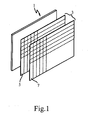
- FIG. 1 is a perspective view of a dual-panel display panel according to an embodiment of the present invention.
- the figure only shows the first display panel 1, and a second display panel 3 formed on the first display panel 3.
- the second display panel 3 includes the second lower plate 5 and the second upper plate 7, with a liquid crystal layer 9 between them.
- the liquid crystal layer 9 may be made from cholesteric liquid crystals.
- a second display panel including a cholesteric liquid crystal layer may be combined with a first display panel, such as the commonly used LCD or PDP, to form a dual-panel display panel or a more advanced flat-panel display.
- a first display panel such as the commonly used LCD or PDP
- LCD or PLD liquid crystal display
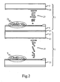
- FIG. 2 is a cross-sectional view of a flat-panel display comprising the dual-panel display panel shown in Fig. 1 according to the first embodiment of the present invention.
- an exemplary embodiment of the present invention includes a first display panel 1, which is an LCD display, and a second display panel 3.
- the first display panel includes a first lower plate 11 having thin-film transistors 9, and a second upper plate 17 having transparent electrodes 13 and a polarizing plate 15.
- a liquid crystal layer 19 lies between the first upper plate 17 and the first lower plate 11.
- the second display panel 3 formed on the first display panel 1 is a liquid crystal display panel, which includes the second lower plate 5 having thin-film transistors 21, and the second upper plate 7 having transparent electrodes 23.
- the second lower plate 5 is connected to the first display panel 1.
- a liquid crystal layer 25 lies between the second upper plate 7 and the second lower plate 5.
- the crystal layer 25 is made from cholesteric liquid crystals.
- the first display panel 1 and the second display panel 3 have corresponding first control circuit and second control circuit respectively (not shown in the drawings).
- the integration of the cholesteric liquid crystal layer 25 and the first display panel 1 requires that their resolutions match, so that the thin-film transistor 21 of the second lower plate 5 and the thin-film transistor 9 of the first lower plate correspond to each other.
- the image produced through the first display panel 1 and the corresponding control circuit needs to be converted to comply with the resolution of the second display panel 3.
- the conversion may be performed by a converting device or a software program.
- first upper plate 17, the second lower plate 5 and the second upper plate 7 are all transparent in order for the first display panel 1 and the second display panel 3 to show the images.
- a main controller (not shown in the drawings) is provided according to exemplary embodiments of the present invention.
- the main controller connects to a first control circuit (not shown in the drawings) and a second control circuit (not shown in the drawings) or is combined with the two circuits to form one single circuit.
- the main controller controls the second control circuit (not shown in the drawings) to adjust the cholesteric liquid crystal layer to open status to let light pass through, and enables the user to select an image from the images shown on the first display panel or saved in a memory device for display on the second display panel.
- FIG. 3 is a cross-sectional view a flat-panel display comprising the dual-panel display panel shown in Fig. 1 according to the second embodiment of the present invention.
- another exemplary embodiment of the present invention includes a first display panel 1, which is DC type PDP, and a second display panel 3.
- the first display panel 1 includes a first lower plate 27 and a first upper plate 29.
- the electrode 31 on the upper plate 29 and the electrode 33 on the first lower plate 27 are arranged in a crisscross pattern.
- the first upper plate 29 has dielectrics 35
- the first lower plate 27 has dielectrics 37.
- the dielectrics 37 on the first lower plate 27 further have a fluorescent material thereon.
- the second display panel 3 formed on the first display panel 1 is a liquid crystal display panel, including a second lower plate 5 having thin-film transistors 21 and the second upper plate 7 having transparent electrodes 23.
- the second lower plate 5 is adjacent and connected to the first display panel 1.
- a liquid crystal layer 25 which is made from cholesteric liquid crystals.
- first display panel 1 and the second display panel 3 have corresponding first control circuit and second control circuit respectively (not shown in drawings).
- a main controller (not shown in drawings) may be connected to the first control circuit and the second control circuit or be combined with them to form a single circuit.
- the main controller controls the second control circuit to adjust the cholesteric liquid crystal layer 25 of the second display panel 3 to the open status to let light pass through, and enables the user to select an image from the images shown on the first display panel or saved in a memory device for display on the second display panel 3.
- the resolutions of the cholesteric liquid crystal layer 25 and the first display panel 1 need to match so that the thin-film transistors 21 of the second lower plate 5 correspond to the X-Y crossly arranged electrodes 31 and 33 of the first upper plate 29 and the first lower plate 27 respectively.
- a converter may be used to adjust the resolution of the image produced from the first display panel 1 and the corresponding control circuit in order to match the resolution of the second display panel 3.
- the thin-film transistors of the flat-panel display cause electromagnetic interference, the thin-film transistors of the cholesteric liquid crystal layer must be reversely adjusted.
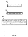
- a flowchart of Fig. 4 shows the method for showing image after the flat-panel display shown in Fig. 2 is turned off.
- the source of the images may be a card reader, a general media (such as a TV set and/or a DVD/VCD player), or a digital camera (Step 401).
- the image is saved in a memory device, which may be installed either within or outside of the flat-panel display (Step 402).
- the images saved in the memory device may be an image obtained from the images shown on the flat-panel display, or an image obtained from a image memory device.
- the image memory device may be a walkman, SD card or other device for saving pictures or images.
- the thin-film transistors of the cholesteric liquid crystals will be turned off, thus cholesteric liquid crystal layer is on the open status. Because the cholesteric liquid crystals are characterized by 360-degree visibility, the normal function of the flat-panel display will not be affected. Further, when the flat-panel display is turned off or when the first display panel does not show images for a while, the main controller may control the second display panel to show an image saved in the memory device. Because of the bistable characteristic of cholesteric liquid crystals, when power is not provided, the image selected will be still show on the display panel. The image may be pre-selected or selected randomly.
- the flat-panel display according to the exemplary embodiments of the present invention can become a beautiful picture instead of a dark and dull scene after the flat-panel display is turned off.
Landscapes
- Engineering & Computer Science (AREA)
- Physics & Mathematics (AREA)
- Computer Hardware Design (AREA)
- General Physics & Mathematics (AREA)
- Theoretical Computer Science (AREA)
- Chemical & Material Sciences (AREA)
- Crystallography & Structural Chemistry (AREA)
- Plasma & Fusion (AREA)
- Liquid Crystal (AREA)
- Control Of Indicators Other Than Cathode Ray Tubes (AREA)
- Devices For Indicating Variable Information By Combining Individual Elements (AREA)
- Liquid Crystal Display Device Control (AREA)
Priority Applications (2)
| Application Number | Priority Date | Filing Date | Title |
|---|---|---|---|
| EP06290726A EP1852731B1 (de) | 2006-05-05 | 2006-05-05 | Doppelbildschirmanzeige, Flachbildschirm mit einer Doppelbildschirmanzeige und Verfahren zur Bildanzeige nach Abschalten des Flachbildschirms |
| AT06290726T ATE511119T1 (de) | 2006-05-05 | 2006-05-05 | Doppelbildschirmanzeige, flachbildschirm mit einer doppelbildschirmanzeige und verfahren zur bildanzeige nach abschalten des flachbildschirms |
Applications Claiming Priority (1)
| Application Number | Priority Date | Filing Date | Title |
|---|---|---|---|
| EP06290726A EP1852731B1 (de) | 2006-05-05 | 2006-05-05 | Doppelbildschirmanzeige, Flachbildschirm mit einer Doppelbildschirmanzeige und Verfahren zur Bildanzeige nach Abschalten des Flachbildschirms |
Publications (2)
| Publication Number | Publication Date |
|---|---|
| EP1852731A1 true EP1852731A1 (de) | 2007-11-07 |
| EP1852731B1 EP1852731B1 (de) | 2011-05-25 |
Family
ID=36950144
Family Applications (1)
| Application Number | Title | Priority Date | Filing Date |
|---|---|---|---|
| EP06290726A Expired - Lifetime EP1852731B1 (de) | 2006-05-05 | 2006-05-05 | Doppelbildschirmanzeige, Flachbildschirm mit einer Doppelbildschirmanzeige und Verfahren zur Bildanzeige nach Abschalten des Flachbildschirms |
Country Status (2)
| Country | Link |
|---|---|
| EP (1) | EP1852731B1 (de) |
| AT (1) | ATE511119T1 (de) |
Cited By (3)
| Publication number | Priority date | Publication date | Assignee | Title |
|---|---|---|---|---|
| WO2010109435A1 (en) * | 2009-03-27 | 2010-09-30 | Koninklijke Philips Electronics N.V. | A device for placement in front of a display device |
| DE102016118416A1 (de) | 2016-09-29 | 2018-03-29 | Thomas Emde | Display |
| EP3588265A1 (de) * | 2018-06-26 | 2020-01-01 | Vestel Elektronik Sanayi ve Ticaret A.S. | Vorrichtung, verfahren und computerprogramm zum erhalt einer anzeige beim einschalten |
Citations (6)
| Publication number | Priority date | Publication date | Assignee | Title |
|---|---|---|---|---|
| EP0516076A2 (de) * | 1991-05-27 | 1992-12-02 | Dainippon Ink And Chemicals, Inc. | Flüssigkristallvorrichtung |
| US6392725B1 (en) * | 1997-11-18 | 2002-05-21 | Fuji Xerox Co., Ltd. | Systems and methods for providing a storage medium |
| US20020176041A1 (en) * | 2001-03-28 | 2002-11-28 | Minolta Co., Ltd. | Liquid crystal display apparatus |
| US20040012836A1 (en) * | 2002-07-16 | 2004-01-22 | Zili Li | Electroptic device |
| WO2004049051A1 (en) * | 2002-11-22 | 2004-06-10 | Koninklijke Philips Electronics N.V. | Transflective liquid crystal display device |
| US20060088667A1 (en) * | 2004-10-26 | 2006-04-27 | Xerox Corporation | Device with multiple liquid crystal layers |
-
2006
- 2006-05-05 EP EP06290726A patent/EP1852731B1/de not_active Expired - Lifetime
- 2006-05-05 AT AT06290726T patent/ATE511119T1/de not_active IP Right Cessation
Patent Citations (6)
| Publication number | Priority date | Publication date | Assignee | Title |
|---|---|---|---|---|
| EP0516076A2 (de) * | 1991-05-27 | 1992-12-02 | Dainippon Ink And Chemicals, Inc. | Flüssigkristallvorrichtung |
| US6392725B1 (en) * | 1997-11-18 | 2002-05-21 | Fuji Xerox Co., Ltd. | Systems and methods for providing a storage medium |
| US20020176041A1 (en) * | 2001-03-28 | 2002-11-28 | Minolta Co., Ltd. | Liquid crystal display apparatus |
| US20040012836A1 (en) * | 2002-07-16 | 2004-01-22 | Zili Li | Electroptic device |
| WO2004049051A1 (en) * | 2002-11-22 | 2004-06-10 | Koninklijke Philips Electronics N.V. | Transflective liquid crystal display device |
| US20060088667A1 (en) * | 2004-10-26 | 2006-04-27 | Xerox Corporation | Device with multiple liquid crystal layers |
Cited By (6)
| Publication number | Priority date | Publication date | Assignee | Title |
|---|---|---|---|---|
| WO2010109435A1 (en) * | 2009-03-27 | 2010-09-30 | Koninklijke Philips Electronics N.V. | A device for placement in front of a display device |
| US8686984B2 (en) | 2009-03-27 | 2014-04-01 | Kkoninklijke Philips N.V. | Device for placement in front of a display device |
| RU2543995C2 (ru) * | 2009-03-27 | 2015-03-10 | Конинклейке Филипс Электроникс Н.В. | Устройство для размещения перед устройством отображения |
| DE102016118416A1 (de) | 2016-09-29 | 2018-03-29 | Thomas Emde | Display |
| EP3588265A1 (de) * | 2018-06-26 | 2020-01-01 | Vestel Elektronik Sanayi ve Ticaret A.S. | Vorrichtung, verfahren und computerprogramm zum erhalt einer anzeige beim einschalten |
| US10666890B2 (en) | 2018-06-26 | 2020-05-26 | Vestel Elektronik Sanayi Ve Ticaret A.S. | Apparatus, method and computer program for obtaining a display at power-on |
Also Published As
| Publication number | Publication date |
|---|---|
| ATE511119T1 (de) | 2011-06-15 |
| EP1852731B1 (de) | 2011-05-25 |
Similar Documents
| Publication | Publication Date | Title |
|---|---|---|
| JP7378618B2 (ja) | 表示パネル | |
| WO2021017931A1 (zh) | 显示面板及显示装置 | |
| CN118865888A (zh) | 显示面板、电子设备以及显示驱动方法 | |
| WO2008012727A1 (en) | Display device | |
| WO2018121303A1 (zh) | 液晶显示器及其驱动方法 | |
| JP2008225413A (ja) | 液晶表示装置 | |
| JP2008009365A (ja) | 液晶表示装置 | |
| TWI718913B (zh) | 顯示方法 | |
| CN112530292B (zh) | 显示面板和显示装置 | |
| US6683417B2 (en) | Organic electro luminescent display device | |
| CN115631724A (zh) | 显示模组及其驱动方法、显示装置 | |
| KR20040071959A (ko) | 액정표시장치 | |
| EP1852731B1 (de) | Doppelbildschirmanzeige, Flachbildschirm mit einer Doppelbildschirmanzeige und Verfahren zur Bildanzeige nach Abschalten des Flachbildschirms | |
| US20070258023A1 (en) | Dual-panel display panel, flat-panel display employing a dual-panel display panel, and method of showing images after the flat-panel display is turned off | |
| CN100430787C (zh) | 双层显示面板及其平面显示器与其关机后图像显示方法 | |
| CN114397781A (zh) | 背光模组及其制备方法和显示装置 | |
| TW200834507A (en) | Method and apparatus for adjusting display response time | |
| KR102623354B1 (ko) | 멀티 비전 장치 및 멀티 비전 장치에 포함된 표시 장치 | |
| US20100103090A1 (en) | Liquid crystal display module and display system including the same | |
| US8659530B2 (en) | Timing controller counts clock signals to produce a control signal only after a number of clock pulses are counted | |
| US20250240894A1 (en) | Display device | |
| CN119446079B (zh) | 显示面板及显示装置 | |
| CN219800460U (zh) | 显示装置 | |
| WO2010018881A1 (en) | Display apparatus for variable picture size | |
| CN102842298B (zh) | 显示反应时间的调整方法 |
Legal Events
| Date | Code | Title | Description |
|---|---|---|---|
| PUAI | Public reference made under article 153(3) epc to a published international application that has entered the european phase |
Free format text: ORIGINAL CODE: 0009012 |
|
| 17P | Request for examination filed |
Effective date: 20060513 |
|
| AK | Designated contracting states |
Kind code of ref document: A1 Designated state(s): AT BE BG CH CY CZ DE DK EE ES FI FR GB GR HU IE IS IT LI LT LU LV MC NL PL PT RO SE SI SK TR |
|
| AX | Request for extension of the european patent |
Extension state: AL BA HR MK YU |
|
| AKX | Designation fees paid |
Designated state(s): AT BE BG CH CY CZ DE DK EE ES FI FR GB GR HU IE IS IT LI LT LU LV MC NL PL PT RO SE SI SK TR |
|
| GRAP | Despatch of communication of intention to grant a patent |
Free format text: ORIGINAL CODE: EPIDOSNIGR1 |
|
| GRAS | Grant fee paid |
Free format text: ORIGINAL CODE: EPIDOSNIGR3 |
|
| GRAA | (expected) grant |
Free format text: ORIGINAL CODE: 0009210 |
|
| AK | Designated contracting states |
Kind code of ref document: B1 Designated state(s): AT BE BG CH CY CZ DE DK EE ES FI FR GB GR HU IE IS IT LI LT LU LV MC NL PL PT RO SE SI SK TR |
|
| REG | Reference to a national code |
Ref country code: GB Ref legal event code: FG4D |
|
| REG | Reference to a national code |
Ref country code: CH Ref legal event code: EP |
|
| REG | Reference to a national code |
Ref country code: IE Ref legal event code: FG4D |
|
| REG | Reference to a national code |
Ref country code: DE Ref legal event code: R096 Ref document number: 602006022161 Country of ref document: DE Effective date: 20110707 |
|
| REG | Reference to a national code |
Ref country code: NL Ref legal event code: T3 |
|
| PG25 | Lapsed in a contracting state [announced via postgrant information from national office to epo] |
Ref country code: PT Free format text: LAPSE BECAUSE OF FAILURE TO SUBMIT A TRANSLATION OF THE DESCRIPTION OR TO PAY THE FEE WITHIN THE PRESCRIBED TIME-LIMIT Effective date: 20110926 Ref country code: SE Free format text: LAPSE BECAUSE OF FAILURE TO SUBMIT A TRANSLATION OF THE DESCRIPTION OR TO PAY THE FEE WITHIN THE PRESCRIBED TIME-LIMIT Effective date: 20110525 Ref country code: LT Free format text: LAPSE BECAUSE OF FAILURE TO SUBMIT A TRANSLATION OF THE DESCRIPTION OR TO PAY THE FEE WITHIN THE PRESCRIBED TIME-LIMIT Effective date: 20110525 |
|
| PG25 | Lapsed in a contracting state [announced via postgrant information from national office to epo] |
Ref country code: GR Free format text: LAPSE BECAUSE OF FAILURE TO SUBMIT A TRANSLATION OF THE DESCRIPTION OR TO PAY THE FEE WITHIN THE PRESCRIBED TIME-LIMIT Effective date: 20110826 Ref country code: BE Free format text: LAPSE BECAUSE OF FAILURE TO SUBMIT A TRANSLATION OF THE DESCRIPTION OR TO PAY THE FEE WITHIN THE PRESCRIBED TIME-LIMIT Effective date: 20110525 Ref country code: SI Free format text: LAPSE BECAUSE OF FAILURE TO SUBMIT A TRANSLATION OF THE DESCRIPTION OR TO PAY THE FEE WITHIN THE PRESCRIBED TIME-LIMIT Effective date: 20110525 Ref country code: LV Free format text: LAPSE BECAUSE OF FAILURE TO SUBMIT A TRANSLATION OF THE DESCRIPTION OR TO PAY THE FEE WITHIN THE PRESCRIBED TIME-LIMIT Effective date: 20110525 Ref country code: AT Free format text: LAPSE BECAUSE OF FAILURE TO SUBMIT A TRANSLATION OF THE DESCRIPTION OR TO PAY THE FEE WITHIN THE PRESCRIBED TIME-LIMIT Effective date: 20110525 Ref country code: ES Free format text: LAPSE BECAUSE OF FAILURE TO SUBMIT A TRANSLATION OF THE DESCRIPTION OR TO PAY THE FEE WITHIN THE PRESCRIBED TIME-LIMIT Effective date: 20110905 Ref country code: IS Free format text: LAPSE BECAUSE OF FAILURE TO SUBMIT A TRANSLATION OF THE DESCRIPTION OR TO PAY THE FEE WITHIN THE PRESCRIBED TIME-LIMIT Effective date: 20110925 Ref country code: CY Free format text: LAPSE BECAUSE OF FAILURE TO SUBMIT A TRANSLATION OF THE DESCRIPTION OR TO PAY THE FEE WITHIN THE PRESCRIBED TIME-LIMIT Effective date: 20110525 Ref country code: FI Free format text: LAPSE BECAUSE OF FAILURE TO SUBMIT A TRANSLATION OF THE DESCRIPTION OR TO PAY THE FEE WITHIN THE PRESCRIBED TIME-LIMIT Effective date: 20110525 |
|
| PG25 | Lapsed in a contracting state [announced via postgrant information from national office to epo] |
Ref country code: EE Free format text: LAPSE BECAUSE OF FAILURE TO SUBMIT A TRANSLATION OF THE DESCRIPTION OR TO PAY THE FEE WITHIN THE PRESCRIBED TIME-LIMIT Effective date: 20110525 Ref country code: CZ Free format text: LAPSE BECAUSE OF FAILURE TO SUBMIT A TRANSLATION OF THE DESCRIPTION OR TO PAY THE FEE WITHIN THE PRESCRIBED TIME-LIMIT Effective date: 20110525 |
|
| PG25 | Lapsed in a contracting state [announced via postgrant information from national office to epo] |
Ref country code: PL Free format text: LAPSE BECAUSE OF FAILURE TO SUBMIT A TRANSLATION OF THE DESCRIPTION OR TO PAY THE FEE WITHIN THE PRESCRIBED TIME-LIMIT Effective date: 20110525 Ref country code: RO Free format text: LAPSE BECAUSE OF FAILURE TO SUBMIT A TRANSLATION OF THE DESCRIPTION OR TO PAY THE FEE WITHIN THE PRESCRIBED TIME-LIMIT Effective date: 20110525 Ref country code: SK Free format text: LAPSE BECAUSE OF FAILURE TO SUBMIT A TRANSLATION OF THE DESCRIPTION OR TO PAY THE FEE WITHIN THE PRESCRIBED TIME-LIMIT Effective date: 20110525 Ref country code: DK Free format text: LAPSE BECAUSE OF FAILURE TO SUBMIT A TRANSLATION OF THE DESCRIPTION OR TO PAY THE FEE WITHIN THE PRESCRIBED TIME-LIMIT Effective date: 20110525 |
|
| PLBE | No opposition filed within time limit |
Free format text: ORIGINAL CODE: 0009261 |
|
| STAA | Information on the status of an ep patent application or granted ep patent |
Free format text: STATUS: NO OPPOSITION FILED WITHIN TIME LIMIT |
|
| 26N | No opposition filed |
Effective date: 20120228 |
|
| REG | Reference to a national code |
Ref country code: DE Ref legal event code: R097 Ref document number: 602006022161 Country of ref document: DE Effective date: 20120228 |
|
| PG25 | Lapsed in a contracting state [announced via postgrant information from national office to epo] |
Ref country code: MC Free format text: LAPSE BECAUSE OF NON-PAYMENT OF DUE FEES Effective date: 20120531 |
|
| REG | Reference to a national code |
Ref country code: CH Ref legal event code: PL |
|
| PG25 | Lapsed in a contracting state [announced via postgrant information from national office to epo] |
Ref country code: CH Free format text: LAPSE BECAUSE OF NON-PAYMENT OF DUE FEES Effective date: 20120531 Ref country code: LI Free format text: LAPSE BECAUSE OF NON-PAYMENT OF DUE FEES Effective date: 20120531 |
|
| REG | Reference to a national code |
Ref country code: IE Ref legal event code: MM4A |
|
| PG25 | Lapsed in a contracting state [announced via postgrant information from national office to epo] |
Ref country code: IE Free format text: LAPSE BECAUSE OF NON-PAYMENT OF DUE FEES Effective date: 20120505 |
|
| PG25 | Lapsed in a contracting state [announced via postgrant information from national office to epo] |
Ref country code: BG Free format text: LAPSE BECAUSE OF FAILURE TO SUBMIT A TRANSLATION OF THE DESCRIPTION OR TO PAY THE FEE WITHIN THE PRESCRIBED TIME-LIMIT Effective date: 20110825 |
|
| PG25 | Lapsed in a contracting state [announced via postgrant information from national office to epo] |
Ref country code: TR Free format text: LAPSE BECAUSE OF FAILURE TO SUBMIT A TRANSLATION OF THE DESCRIPTION OR TO PAY THE FEE WITHIN THE PRESCRIBED TIME-LIMIT Effective date: 20110525 |
|
| PG25 | Lapsed in a contracting state [announced via postgrant information from national office to epo] |
Ref country code: LU Free format text: LAPSE BECAUSE OF NON-PAYMENT OF DUE FEES Effective date: 20120505 |
|
| PG25 | Lapsed in a contracting state [announced via postgrant information from national office to epo] |
Ref country code: HU Free format text: LAPSE BECAUSE OF FAILURE TO SUBMIT A TRANSLATION OF THE DESCRIPTION OR TO PAY THE FEE WITHIN THE PRESCRIBED TIME-LIMIT Effective date: 20060505 |
|
| REG | Reference to a national code |
Ref country code: FR Ref legal event code: PLFP Year of fee payment: 10 |
|
| REG | Reference to a national code |
Ref country code: FR Ref legal event code: PLFP Year of fee payment: 11 |
|
| REG | Reference to a national code |
Ref country code: FR Ref legal event code: PLFP Year of fee payment: 12 |
|
| REG | Reference to a national code |
Ref country code: FR Ref legal event code: PLFP Year of fee payment: 13 |
|
| REG | Reference to a national code |
Ref country code: FR Ref legal event code: PLFP Year of fee payment: 18 |
|
| PGFP | Annual fee paid to national office [announced via postgrant information from national office to epo] |
Ref country code: GB Payment date: 20230330 Year of fee payment: 18 |
|
| PGFP | Annual fee paid to national office [announced via postgrant information from national office to epo] |
Ref country code: NL Payment date: 20230417 Year of fee payment: 18 |
|
| PGFP | Annual fee paid to national office [announced via postgrant information from national office to epo] |
Ref country code: IT Payment date: 20230412 Year of fee payment: 18 Ref country code: FR Payment date: 20230411 Year of fee payment: 18 Ref country code: DE Payment date: 20230331 Year of fee payment: 18 |
|
| REG | Reference to a national code |
Ref country code: DE Ref legal event code: R119 Ref document number: 602006022161 Country of ref document: DE |
|
| REG | Reference to a national code |
Ref country code: NL Ref legal event code: MM Effective date: 20240601 |
|
| GBPC | Gb: european patent ceased through non-payment of renewal fee |
Effective date: 20240505 |
|
| PG25 | Lapsed in a contracting state [announced via postgrant information from national office to epo] |
Ref country code: NL Free format text: LAPSE BECAUSE OF NON-PAYMENT OF DUE FEES Effective date: 20240601 |
|
| PG25 | Lapsed in a contracting state [announced via postgrant information from national office to epo] |
Ref country code: DE Free format text: LAPSE BECAUSE OF NON-PAYMENT OF DUE FEES Effective date: 20241203 |
|
| PG25 | Lapsed in a contracting state [announced via postgrant information from national office to epo] |
Ref country code: FR Free format text: LAPSE BECAUSE OF NON-PAYMENT OF DUE FEES Effective date: 20240531 |
|
| PG25 | Lapsed in a contracting state [announced via postgrant information from national office to epo] |
Ref country code: GB Free format text: LAPSE BECAUSE OF NON-PAYMENT OF DUE FEES Effective date: 20240505 Ref country code: IT Free format text: LAPSE BECAUSE OF NON-PAYMENT OF DUE FEES Effective date: 20240505 |