EP1852973A1 - Filtre d onde acoustique superficielle équilibrée - Google Patents
Filtre d onde acoustique superficielle équilibrée Download PDFInfo
- Publication number
- EP1852973A1 EP1852973A1 EP05844788A EP05844788A EP1852973A1 EP 1852973 A1 EP1852973 A1 EP 1852973A1 EP 05844788 A EP05844788 A EP 05844788A EP 05844788 A EP05844788 A EP 05844788A EP 1852973 A1 EP1852973 A1 EP 1852973A1
- Authority
- EP
- European Patent Office
- Prior art keywords
- acoustic wave
- wave filter
- surface acoustic
- idts
- electrode fingers
- Prior art date
- Legal status (The legal status is an assumption and is not a legal conclusion. Google has not performed a legal analysis and makes no representation as to the accuracy of the status listed.)
- Withdrawn
Links
Images


Classifications
-
- H—ELECTRICITY
- H03—ELECTRONIC CIRCUITRY
- H03H—IMPEDANCE NETWORKS, e.g. RESONANT CIRCUITS; RESONATORS
- H03H9/00—Networks comprising electromechanical or electro-acoustic elements; Electromechanical resonators
- H03H9/46—Filters
- H03H9/64—Filters using surface acoustic waves
-
- H—ELECTRICITY
- H03—ELECTRONIC CIRCUITRY
- H03H—IMPEDANCE NETWORKS, e.g. RESONANT CIRCUITS; RESONATORS
- H03H9/00—Networks comprising electromechanical or electro-acoustic elements; Electromechanical resonators
- H03H9/0023—Networks for transforming balanced signals into unbalanced signals and vice versa, e.g. baluns, or networks having balanced input and output
- H03H9/0028—Networks for transforming balanced signals into unbalanced signals and vice versa, e.g. baluns, or networks having balanced input and output using surface acoustic wave devices
- H03H9/0085—Networks for transforming balanced signals into unbalanced signals and vice versa, e.g. baluns, or networks having balanced input and output using surface acoustic wave devices having four acoustic tracks
-
- H—ELECTRICITY
- H03—ELECTRONIC CIRCUITRY
- H03H—IMPEDANCE NETWORKS, e.g. RESONANT CIRCUITS; RESONATORS
- H03H9/00—Networks comprising electromechanical or electro-acoustic elements; Electromechanical resonators
- H03H9/0023—Networks for transforming balanced signals into unbalanced signals and vice versa, e.g. baluns, or networks having balanced input and output
- H03H9/0028—Networks for transforming balanced signals into unbalanced signals and vice versa, e.g. baluns, or networks having balanced input and output using surface acoustic wave devices
- H03H9/0047—Networks for transforming balanced signals into unbalanced signals and vice versa, e.g. baluns, or networks having balanced input and output using surface acoustic wave devices having two acoustic tracks
- H03H9/0066—Networks for transforming balanced signals into unbalanced signals and vice versa, e.g. baluns, or networks having balanced input and output using surface acoustic wave devices having two acoustic tracks being electrically parallel
- H03H9/0071—Networks for transforming balanced signals into unbalanced signals and vice versa, e.g. baluns, or networks having balanced input and output using surface acoustic wave devices having two acoustic tracks being electrically parallel the balanced terminals being on the same side of the tracks
-
- H—ELECTRICITY
- H03—ELECTRONIC CIRCUITRY
- H03H—IMPEDANCE NETWORKS, e.g. RESONANT CIRCUITS; RESONATORS
- H03H9/00—Networks comprising electromechanical or electro-acoustic elements; Electromechanical resonators
- H03H9/02—Details
- H03H9/02535—Details of surface acoustic wave devices
- H03H9/02637—Details concerning reflective or coupling arrays
- H03H9/02685—Grating lines having particular arrangements
- H03H9/0274—Intra-transducers grating lines
- H03H9/02748—Dog-legged reflectors
-
- H—ELECTRICITY
- H03—ELECTRONIC CIRCUITRY
- H03H—IMPEDANCE NETWORKS, e.g. RESONANT CIRCUITS; RESONATORS
- H03H9/00—Networks comprising electromechanical or electro-acoustic elements; Electromechanical resonators
- H03H9/02—Details
- H03H9/125—Driving means, e.g. electrodes, coils
- H03H9/145—Driving means, e.g. electrodes, coils for networks using surface acoustic waves
- H03H9/14544—Transducers of particular shape or position
- H03H9/14576—Transducers whereby only the last fingers have different characteristics with respect to the other fingers, e.g. different shape, thickness or material, split finger
- H03H9/14582—Transducers whereby only the last fingers have different characteristics with respect to the other fingers, e.g. different shape, thickness or material, split finger the last fingers having a different pitch
-
- H—ELECTRICITY
- H03—ELECTRONIC CIRCUITRY
- H03H—IMPEDANCE NETWORKS, e.g. RESONANT CIRCUITS; RESONATORS
- H03H9/00—Networks comprising electromechanical or electro-acoustic elements; Electromechanical resonators
- H03H9/25—Constructional features of resonators using surface acoustic waves
-
- H—ELECTRICITY
- H03—ELECTRONIC CIRCUITRY
- H03H—IMPEDANCE NETWORKS, e.g. RESONANT CIRCUITS; RESONATORS
- H03H9/00—Networks comprising electromechanical or electro-acoustic elements; Electromechanical resonators
- H03H9/46—Filters
- H03H9/64—Filters using surface acoustic waves
- H03H9/6423—Means for obtaining a particular transfer characteristic
- H03H9/6433—Coupled resonator filters
- H03H9/644—Coupled resonator filters having two acoustic tracks
- H03H9/6456—Coupled resonator filters having two acoustic tracks being electrically coupled
- H03H9/6469—Coupled resonator filters having two acoustic tracks being electrically coupled via two connecting electrodes
- H03H9/6476—Coupled resonator filters having two acoustic tracks being electrically coupled via two connecting electrodes the tracks being electrically parallel
-
- H—ELECTRICITY
- H03—ELECTRONIC CIRCUITRY
- H03H—IMPEDANCE NETWORKS, e.g. RESONANT CIRCUITS; RESONATORS
- H03H9/00—Networks comprising electromechanical or electro-acoustic elements; Electromechanical resonators
- H03H9/02—Details
- H03H9/0222—Details of interface-acoustic, boundary, pseudo-acoustic or Stonely wave devices
Definitions
- the present invention relates to balanced acoustic wave filter devices using surface acoustic waves or boundary acoustic waves, and more particularly, to a balanced acoustic wave filter device including first and second longitudinally coupled resonator-type acoustic wave filter sections and having a balanced-to-unbalanced conversion function.
- surface acoustic wave filters are often connected as band-pass filters between antennas and differential amplifiers.
- unbalanced signals are input or output to an antenna.
- balanced signals are input or output to a differential amplifier.
- a component part having an unbalanced-to-balanced conversion function that is, a balun, must be inserted between the antenna and the differential amplifier. If a surface acoustic wave filter having a balanced-to-unbalanced conversion function is used as the above-mentioned band-pass filter, the balun can be omitted.
- various balanced surface acoustic wave filters having the balanced-to-unbalanced conversion function have been proposed.
- Patent Document 1 discloses a balanced surface acoustic wave filter device whose electrode structure is shown by a schematic plan view illustrated in Fig. 14.
- a balanced surface acoustic wave filter device 501 electrodes are formed on a piezoelectric substrate. That is, the electrodes are provided to form a first longitudinally coupled resonator-type surface acoustic wave filter section 502 and a second longitudinally coupled resonator-type surface acoustic wave filter section 503.
- the first surface acoustic wave filter section 502 includes first to third IDTs 511 to 513 disposed along a surface-acoustic-wave propagation direction.
- the second surface acoustic wave filter section 503 also includes fourth to sixth IDTs 514 to 516 disposed along the surface-acoustic-wave propagation direction.
- Reflectors 517a and 517b are provided on both sides in the surface-acoustic-wave propagation direction of an area in which the IDTs 511 to 513 are disposed.
- reflectors 518a and 518b are provided on both sides in the surface-acoustic-wave propagation direction of an area in which the IDTS 514 to 516 are disposed.
- the surface acoustic wave filter sections 502 and 503 are longitudinally coupled resonator-type surface acoustic wave filter sections each formed by three IDTs having the above-mentioned electrode structure.
- first ends of the IDTs 512 and 515 which are disposed at the centers of the first and second surface acoustic wave filter sections 502 and 503, respectively, are connected to an unbalanced terminal 504. Second ends of the IDTs 512 and 515 are connected to a ground potential.
- First ends of the IDTs 511 and 513 are commonly connected to a first balanced terminal 505. Second ends of the IDTs 511 and 513 are connected to the ground potential. In contrast, first ends of the IDTs 514 and 516, which are disposed on both sides in the second surface acoustic wave filter section 503, are commonly connected to a second balanced terminal 506. Second ends of the IDTs 514 and 516 are connected to the ground potential.
- the phase of the IDT 512 is opposite to the phase of the IDT 515.
- the phase of a signal flowing to the first balanced terminal 505 differs from the phase of a signal flowing to the second balanced terminal 506 by 180 degrees.
- Patent Document 1 Japanese Unexamined Patent Application Publication No. 2003-78387 .
- the polarities of a pair of adjacent electrode fingers differ between the first surface acoustic wave filter section 502 and the second surface acoustic wave filter section 503.
- each of the electrode fingers that are adjacent to each other across a gap between the IDTs 511 and 512 is connected to a corresponding signal terminal
- each of the electrode fingers that are adjacent to each other across a gap between the IDTS 512 and 513 is connected to a corresponding signal terminal.
- surface acoustic waves are not excited very strongly between the IDTs 511 and 512 and between the IDTs 512 and 513.
- one of the electrode fingers that face each other through a gap between the IDTs 514 and 515 in the second surface acoustic wave filter section 503 is connected to a signal terminal, and the other one of the electrode fingers is connected to the ground potential.
- one of the electrode fingers that are adjacent to each other between the IDTs 515 and 516 is connected to the ground potential, and the other one of the electrode fingers is connected to a signal terminal.
- the excitation states of surface acoustic waves in gaps in the first longitudinally coupled resonator-type surface acoustic wave filter section 502 and the second longitudinally coupled resonator-type surface acoustic wave filter section 503 differ from each other. This causes a difference in bandwidths and deteriorates the VSWR and the insertion loss in the pass band.
- An object of the present invention is that it overcomes the above-mentioned drawbacks of the related art and provides a balanced surface acoustic wave filter device having a balanced-to-unbalanced conversion function, including first and second longitudinally coupled resonator-type surface acoustic wave filter sections connected to an unbalanced terminal, and having a structure capable of reducing the insertion loss and the VSWR in a pass band.
- a balanced acoustic wave filter device including a piezoelectric substrate and first and second longitudinally coupled resonator-type acoustic wave filter sections formed on the piezoelectric substrate, each of the first and second acoustic wave filter sections including a plurality of IDTs disposed in a direction in which surface acoustic waves propagate.
- An input or an output of each of the first and second acoustic wave filter sections is connected to an unbalanced terminal, the output or the input of the first acoustic wave filter section is connected to a first balanced terminal, the output or the input of the second acoustic wave filter section is connected to a second balanced terminal, and the phase of a signal of the output or the input of the first acoustic wave filter section is different from the phase of a signal of the output or the input of the second acoustic wave filter section by 180 degrees.
- the polarities of electrode fingers that are adjacent to each other in an area in which the IDTs are adjacent to each other in a direction in which acoustic waves propagate are equal to each other
- the polarities of electrode fingers that are adjacent to each other in an area in which the IDTs are adjacent to each other are opposite to each other.
- the total number of pairs of electrode fingers in the second acoustic wave filter section is greater than the total number of pairs of electrode fingers in the first acoustic wave filter section.
- the balanced acoustic wave filter device may further include at least one third longitudinally coupled resonator-type surface acoustic wave filter section that is connected in a cascade arrangement to the first acoustic wave filter section and at least one fourth longitudinally coupled resonator-type surface acoustic wave filter section that is connected in a cascade arrangement to the second acoustic wave filter section.
- each of the IDTS may include a narrow-pitched electrode finger portion having an electrode finger pitch that is narrower than an electrode finger pitch of the other portions of the corresponding IDT.
- surface acoustic waves may be used as the acoustic waves, and a surface acoustic wave filter device may be configured using the surface acoustic waves.
- boundary acoustic waves may be used as the acoustic waves, and a boundary acoustic wave filter device may be configured using the boundary acoustic waves.
- the input or the output of each of the first and second acoustic wave filter sections is connected to the unbalanced terminal, the output or the input of the first acoustic wave filter section is connected to the first balanced terminal, the output or the input of the second acoustic wave filter section is connected to the second balanced terminal, and the phase of the signal of the output or the input of the first acoustic wave filter section is different from the phase of the signal of the output or the input of the second acoustic wave filter section by 180 degrees.
- the balanced acoustic wave filter device having a balanced-to-unbalanced conversion function can be provided.
- the total number of pairs of electrode fingers in the second acoustic wave filter section in which the polarities of the electrode fingers that are adjacent to each other in the area in which the IDTs are adjacent to each other are opposite to each other is greater than the total number of pairs of electrode fingers in the first acoustic wave filter section in which the polarities of the electrode fingers that are adjacent to each other in the area in which the IDTS are adjacent to each other in the direction in which the acoustic waves propagate are ground and ground or hot and hot.
- the insertion loss in the pass band needs to be as small as possible for band-pass filters used in mobile communication apparatuses and the like.
- even an improvement of about 0.1 dB in insertion loss attains a significant advantage in the reduction of insertion loss.
- the insertion loss in the pass band can be effectively improved.
- an opportunity to use a balanced acoustic wave filter device as a band-pass filter of a communication apparatus or the like can be further enhanced.
- At least one third longitudinally coupled resonator-type surface acoustic wave filter section and at least one fourth longitudinally coupled resonator-type surface acoustic wave filter section that are connected in a cascade arrangement to the first and second acoustic wave filter sections, respectively, are provided, an attenuation outside the band can be increased.
- each of the IDTs includes a narrow-pitched electrode finger portion having an electrode finger pitch that is narrower than an electrode finger pitch of the other portions of the corresponding IDT, discontinuity in the areas in which the IDTs are adjacent to each other can be reduced. Thus, the insertion loss in the band can be further reduced.
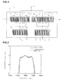
- Fig. 1 is a schematic plan view showing a balanced surface acoustic wave filter device according to a first embodiment of the present invention.
- a balanced surface acoustic wave filter device 1 has an electrode structure shown in Fig. 1 formed on a piezoelectric substrate 2.
- the piezoelectric substrate 2 is a piezoelectric substrate made of 40 ⁇ 5-degree Y-cut, X-propagating LiTaO3.
- the piezoelectric substrate may be made of other types of piezoelectric single crystal or piezoelectric ceramics.
- the piezoelectric substrate may be configured such that a piezoelectric thin film is formed on the surface of a piezoelectric material or an insulating material.
- the electrodes are made of aluminum in this embodiment, the electrodes may be made of aluminum alloy, other types of metal, or other types of alloy. In addition, the electrodes may be formed by laminating a plurality of electrode layers.
- the balanced surface acoustic wave filter device 1 includes an unbalanced terminal 3 and first and second balanced terminals 4 and 5.
- First and second longitudinally coupled resonator-type surface acoustic wave filter sections 6 and 7 are connected in parallel to the unbalanced terminal 3.
- the first surface acoustic wave filter section 6 is a longitudinally coupled resonator-type surface acoustic wave filter section having three IDTs, first to third IDTs 11 to 13, disposed along a direction in which surface acoustic waves propagate.
- the IDT 12 disposed in the middle is electrically connected to the above-described unbalanced terminal 3.
- Reflectors 17a and 17b are disposed on both sides in the direction in which surface acoustic waves propagate of an area in which the IDTs 11 to 13 are provided.
- Second ends of the first and third IDTs 11 and 13 are connected to the ground potential.
- An end of the second IDT 12 that is opposite to the end connected to the unbalanced terminal 3 is connected to the ground potential.
- the second longitudinally coupled resonator-type surface acoustic wave filter section 7 includes fourth to sixth IDTs 14 to 16 disposed in the direction in which surface acoustic waves propagate.
- the fifth IDT 15 disposed in the middle is connected to the unbalanced terminal 3.
- An opposite end of the IDT 15 is connected to the ground potential.
- First ends of the IDTs 14 and 16 are commonly connected to the second balanced terminal 5 with a surface acoustic wave resonator 9 therebetween.
- Second ends of the IDTS 14 and 16 are connected to the ground potential.
- Reflectors 18a and 18b are disposed on both sides in the direction in which surface acoustic waves propagate of an area in which the IDTs 14 to 16 are provided.
- the phase of the fifth IDT 15 is opposite to the phase of the second IDT 12.
- the phase of a signal extracted from the first balanced terminal 4 is different from the phase of a signal extracted from the second balanced terminal 5 by 180 degrees. Accordingly, a balanced-to-unbalanced conversion function is realized.
- the IDTs each include a narrow-pitched electrode finger portion in an area in which the IDTs are adjacent to each other.
- the structure of a narrow-pitched electrode finger potion N which is typified by an area in which the IDT 11 and the IDT 12 are adjacent to each other, will now be described.
- the pitch of at least two electrode fingers from an end of the IDT 11 near the IDT 12 is smaller than the pitches of the other electrode fingers of the IDT 11.
- the at least two electrode fingers having the narrow electrode finger pitch constitute the narrow-pitched electrode finger portion N.
- the narrow-pitched electrode finger portion N is also provided in an end of the IDT 12 near the IDT 11. Since the narrow-pitched electrode finger portions N are provided, the discontinuity in propagation of surface acoustic waves in the gap between the IDT 11 and the IDT 12 can be reduced. Thus, the insertion loss in a pass band can be further reduced.
- a narrow-pitched electrode finger portion N is not necessarily provided in an area in which IDTs are adjacent to each other.
- a feature of the surface acoustic wave device 1 according to this embodiment is that the total number of pairs of electrode fingers in the second surface acoustic wave filter section 7 is greater than the total number of pairs of electrode fingers in the first surface acoustic wave filter section 6 and that the insertion loss and the VSWR in the pass band are thus reduced. This feature will be described in more details with reference to Figs. 2 to 7.
- the surface acoustic wave filter device 1 was prepared in accordance with the specifications given below.
- the piezoelectric substrate 2 is a 40 ⁇ 5-degree Y-cut, X-propagating LiTaO3 substrate.
- IDT 11 8.5/(1.5)
- IDT 12 (1.5)/13.0/(1.5)
- IDT 13 (1.5)/8.5.
- the numbers of pairs of electrode fingers shown in parentheses represent the numbers of pairs of electrode fingers in the narrow-pitched electrode finger portions N
- the numbers of pairs of electrode fingers not shown in parentheses represent the numbers of pairs of electrode fingers in electrode finger portions other than the narrow-pitched electrode finger portions N.
- IDT 8.5/(2.5)
- IDT 15 (1.5)/13.0/(1.5)
- IDT 16 (2.5)/8.5.
- the numbers of pairs of electrode fingers shown in parentheses represent the numbers of pairs of electrode fingers in the narrow-pitched electrode finger portions N
- the numbers of pairs of electrode fingers not shown in parentheses represent the numbers of pairs of electrode fingers in electrode finger portions other than the narrow-pitched electrode finger portions N.
- the cross width of electrode fingers of the IDT 8 is 29.3 ⁇ 3
- the cross width of electrode fingers of the IDT 9 is 43.1 ⁇ 3.
- the total number of pairs of electrode fingers of the IDTs in the first surface acoustic wave filter section 6 is 39, and the total number of pairs of electrode fingers of the IDTs in the second surface acoustic wave filter section 7 is 41.
- the sum of the numbers of pairs of electrode fingers of respective IDTs is not necessarily equal to the total number of pairs of electrode fingers of the IDTs in the surface acoustic wave filter section calculated as described above.
- the total number of pairs of electrode fingers of IDTs is taken into consideration since the total number of pairs of electrode fingers affects a bandwidth and a characteristic in a pass band.
- the attenuation-frequency characteristics are represented by the solid line shown in Fig. 2
- the VSWR characteristics near the unbalanced terminal are represented by the solid line shown in Fig. 3
- the VSWR characteristics near the balanced terminals are represented by the solid line shown in Fig. 4.
- a surface acoustic wave filter device according to Comparative Example 1 was prepared in accordance with the following manner, and the attenuation-frequency characteristics and the VSWR characteristics were observed.
- Broken lines shown in Figs. 2 to 4 represent observation results of Comparative Example 1.
- Comparative Example 1 was prepared to be similar to the surface acoustic wave filter device 1 according to the foregoing embodiment with the exception of the points described below.
- the numbers of pairs of electrode fingers of the fourth to sixth IDTs 14 to 16 were changed as described below. That is, the number of pairs of electrode fingers of the IDT 14 is 7.5/(2.5), the number of pairs of electrode fingers of the IDT 15 is (1.5)/13.0/(1.5), and the number of pairs of electrode fingers of the IDT 16 is (2.5)/7.5. Since the total number of pairs of electrode fingers of the IDTs in the second surface acoustic wave filter section 7 is 79, the total number of pairs of electrode fingers is 39, which is equal to the total number of pairs of electrode fingers of the first longitudinally coupled resonator-type surface acoustic wave filter section 6, which is 39. In addition, the cross width of the electrode fingers of the surface acoustic wave resonator 9 is set to be equal to the cross width of the electrode fingers of the surface acoustic wave resonator 8.
- the insertion loss in a pass band that is, the maximum insertion loss in the pass band
- the maximum insertion loss is improved to 1.2 dB, which means an improvement of 0.1 dB, in the surface acoustic wave filter device 1 according to the foregoing embodiment.
- the improvement of the insertion loss in the pass band of 0.1 dB is significantly important for the use of a band-pass filter of a mobile communication apparatus.
- the improvement of 0.1 dB is a huge improvement in the characteristics.
- the total number of pairs in the second surface acoustic wave filter section 7 in which the polarities of electrode fingers that are adjacent to each other in an area in which the IDTS 14 to 16 are adjacent to each other are opposite to each other is greater than the total number of pairs of electrode fingers in the first surface acoustic wave filter section 6 in which the polarities of electrode fingers that are adjacent to each other in an area in which IDTs are adjacent to each other in a direction in which surface acoustic waves propagate are equal to each other, the insertion loss and the VSWR in the pass band can be effectively improved.
- the insertion loss and the VSWR can be improved. Such improvements are caused by the reasons described below.
- a design parameter for the first surface acoustic wave filter section 6 is the same as a design parameter for the second surface acoustic wave filter section 7, the filter characteristics, in particular, the bandwidth of the first surface acoustic wave filter section differs from the filter characteristics, that is, the bandwidth of the second surface acoustic wave filter section 7.
- the bandwidth of the second surface acoustic wave filter section 7 is increased.
- Comparative Example 1 in the second surface acoustic wave filter section 7, the concentration of the impedance is reduced, the VSWR is deteriorated, and the insertion loss is increased.
- the filter characteristics, in particular, the bandwidth of the second surface acoustic wave filter section 7 approaches the bandwidth of the first surface acoustic wave filter section 6.
- the VSWR and the insertion loss in the pass band can be improved as described above.
- An advantage of the present invention can be achieved not by setting the other design parameters to be different, but by setting the total numbers of pairs of electrode fingers of the IDTs in the first surface acoustic wave filter section 6 and the second surface acoustic wave filter section 7 to be different from each other. This will be described below.
- each of the total numbers of pairs of electrode fingers of the IDTs in the first surface acoustic wave filter 6 and the second surface acoustic wave filter device 7 is set to 39, and the other design parameters for the first surface acoustic wave filter section 6, the second surface acoustic wave filter section 7, and the surface acoustic wave resonators 8 and 9 are optimized in accordance with the total numbers of pairs of electrode fingers of the IDTs.
- a surface acoustic wave filter device was prepared in accordance with the manner described below. That is, the numbers of pairs of electrode fingers of the IDTs in the first and second surface acoustic wave filter sections 6 and 7 are equal to the total number of pairs of electrode fingers in the surface acoustic wave filter section 7 according to the foregoing embodiment, which is 41. In addition, the other design parameters are optimized in accordance with the total number of pairs of electrode fingers in the surface acoustic wave filter section 7 according to the foregoing embodiment.
- Figs. 5 to 7 The filter characteristics of the surface acoustic wave filter device according to Comparative Example 2 configured similarly to the foregoing embodiment with the exception of the above-mentioned structure are shown in Figs. 5 to 7, together with the filter characteristics of the surface acoustic wave filter device according to the foregoing embodiment.
- the solid line represents the characteristics of the surface acoustic wave filter device 1 according to the foregoing embodiment
- the broken line represents the characteristics of the surface acoustic wave filter device according to Comparative Example 2.
- Fig. 5 shows the attenuation-frequency characteristics
- Fig. 6 shows the VSWR characteristics near the unbalanced terminals
- Fig. 7 shows the VSWR characteristics near the balanced terminals.
- a lower insertion loss in a pass band and an excellent VSWR characteristic can be achieved in the surface acoustic wave filter device 1 according to the foregoing embodiment. That is, as is clear from results shown in Figs. 2 to 4 and results shown in Figs. 5 to 7, the advantage of the reduction in the insertion loss in the pass band is achieved by not setting the other design parameters to be differ, but by setting the total number of pairs of electrode fingers of the IDTs in the first surface acoustic wave filter section 6 to be different from the total number of pairs of electrode fingers in the second surface acoustic wave filter section 7.
- each of the number of pairs in the fourth IDT 14 and the number of pairs in the sixth IDT 16 is increased by 1.
- one of the number of pairs in the fourth IDT and the number of pairs in the sixth IDT may be increased by 2.
- parameters other than the number of pairs are also asymmetrical between left and right.
- only the number of pairs in the fifth IDT 15 may be increased by 2.
- Fig. 8 is a schematic plan view showing an electrode structure of a surface acoustic wave filter device according to a second embodiment of the present invention.
- first and second longitudinally coupled resonator-type surface acoustic wave filter sections 26 and 27 each formed by three IDTs are connected to the unbalanced terminal 3.
- This embodiment is different from the first embodiment in that although electrode fingers that are connected to the ground potential are adjacent to each other across a gap therebetween in an area in which the IDTs 11 to 13 in the first surface acoustic wave filter section 6 are adjacent to each other in the surface acoustic wave filter device 1 according to the first embodiment, each of the electrode fingers that are disposed on both sides of an area in which the IDTs are adjacent to each other is connected to a signal terminal in an area in which first to third IDTs 31 to 33 in the first surface acoustic wave filter section 26 are disposed in the second embodiment.
- each of an electrode finger 31a of the IDT 31, which is near the IDT 32, and an outermost electrode finger 32a of the IDT 32, which is near the IDT 31, is connected to the balanced terminal 4 or the unbalanced terminal 3. That is, each of the outermost electrode fingers that are adjacent to each other across a gap therebetween is connected to a signal terminal.
- the surface acoustic wave filter device 21 has a similar structure to the surface acoustic wave filter device 1 with the exception described above. Thus, the same parts as in the surface acoustic wave filter device 1 are referred to with similar reference numerals, and the explanations of those same parts will be omitted.
- the bandwidths of the two filter sections 6 and 7 approach each other, thus improving the VSWR and the insertion loss.
- each of the electrode fingers that are adjacent to each other across a gap between IDTs is connected to a signal terminal in the first surface acoustic wave filter section 26, and one of electrode fingers that are adjacent to each other across a gap between IDTS is connected to the ground potential and the other one of the electrode fingers is connected to a signal terminal in the second surface acoustic wave filter section.
- the bandwidth of the second surface acoustic wave filter section 27 is larger than the bandwidth of the first surface acoustic wave filter section 26.
- the total number of pairs of electrode fingers of the IDTs in the second surface acoustic wave filter section 27 is set to be greater than the total number of pairs of electrode fingers of the IDTs in the first surface acoustic wave filter section 26.
- the bandwidth of the second surface acoustic wave filter section 27 approaches the bandwidth of the first surface acoustic wave filter section 26.
- An acoustic wave filter device is not limited to the structure of the first or second embodiment. Various modifications can be made to the present invention.
- Fig. 9 is a schematic plan view of a modification of the surface acoustic wave filter device 1 according to the first embodiment.
- a surface acoustic wave filter device 41 is configured similarly to the first surface acoustic wave filter device 1 with the exception that a fifth IDT 15A in the middle is subjected to a series weighting in a second surface acoustic wave filter section 7A.
- the series weighting is a method for assigning weights to a plurality of electrode fingers including the outermost electrode fingers such that floating electrode fingers 42 and 43 are disposed in positions where the outermost electrode finger and at least one neighboring electrode finger of the IDT 15A are provided. With such a series weighting, the bandwidth of the second surface acoustic wave filter section 7A can be further adjusted.
- the bandwidth of the second surface acoustic wave filter section 7A can be closer to the bandwidth of the first surface acoustic wave filter section 6 by the above-mentioned series weighting.
- various types of weighting such as a series weighting, may be adopted, in addition to setting the total number of pairs of electrode fingers in the second surface acoustic wave filter section to be greater than the total number of pairs of electrode fingers of the IDTs in the first surface acoustic wave filter section.
- a series weighting for example, a withdrawal weighting or an apodization weighting may be adopted.
- Fig. 10 is a schematic plan view of an electrode structure of a surface acoustic wave filter device according to another modification of the surface acoustic wave filter device 1 according to the first embodiment.
- the number of electrode fingers of each of the IDTs 12 and 15 in the middle in the first and second surface acoustic wave filter sections 6 and 7 is odd.
- the number of electrode fingers of each of the second and fifth IDTs 12B and 15B is even.
- the surface acoustic wave filter device 51 is configured similarly to the surface acoustic wave device 1 with the exception of the above-mentioned point.
- electrode fingers that are connected to the ground potential are adjacent to each other across a gap therebetween in an area in which the IDT 11 and an IDT 12B are adjacent to each other in the first surface acoustic wave filter section, and each of electrode fingers that are adjacent to each other across a gap therebetween in an area in which the IDT 12B and the IDT 13 are adjacent to each other is connected to a signal terminal.
- an electrode finger that is connected to the ground potential and an electrode finger that is connected to a signal terminal are adjacent to each other in an area in which IDTS are adjacent to each other in the second surface acoustic wave filter section 7.
- a pair of electrode fingers is not necessarily connected to the ground potential.
- Each of the pair of electrode fingers may be connected to a signal terminal as long as the polarities of electrode fingers that are adjacent to each other across a gap therebetween are the same in an area in which IDTs are adjacent to each other.
- the bandwidths of the first surface acoustic wave filter section 6 and the second surface acoustic wave filter section 7 approach each other.
- the insertion loss and the VSWR in a pass band can be improved as in the first surface acoustic wave filter device 1.
- Fig. 11 is a schematic plan view of an electrode structure of a surface acoustic wave filter device according to a third embodiment of the present invention.
- first and second surface acoustic wave filter sections 66 and 67 are longitudinally coupled resonator-type surface acoustic wave filter sections including first to fifth IDTs 71 to 75 and sixth to tenth IDTs 76 to 80, respectively.
- the surface acoustic wave filter device 61 is configured similarly to the surface acoustic wave filter device 1 with the exception of the above-mentioned point.
- the first and second surface acoustic wave filter sections may be longitudinally coupled resonator-type surface acoustic wave filter sections each formed by five IDTs.
- the total number of pairs of electrode fingers of the IDTs in the second longitudinally coupled resonator-type surface acoustic wave filter section 67 is set to be greater than the total number of pairs of electrode fingers of the IDTs in the first surface acoustic wave filter section 66.
- Fig. 12 is a schematic plan view of an electrode structure of a surface acoustic wave filter device according to a fourth embodiment of the present invention.
- a surface acoustic wave filter device 81 shown in Fig. 12 longitudinally coupled resonator-type surface acoustic wave filter sections 82 and 83 each formed by three IDTs are connected in a cascade arrangement downstream of the first and second surface acoustic wave filter sections 6 and 7, respectively, of the surface acoustic wave filter device 1 according to the first embodiment.
- the total number of pairs of electrode fingers in the second surface acoustic wave filter section 7 is set to be greater than the total number of pairs of electrode fingers of the IDTs in the first surface acoustic wave filter section 6, that is, if the surface acoustic wave filter device is configured similarly to the surface acoustic wave filter device 1 according to the first embodiment, improvements in the insertion loss and the VSWR in the pass band can be achieved. That is, the total number of pairs of electrode fingers in the surface acoustic wave filter section 82 may be equal to the total number of pairs of electrode fingers in the surface acoustic wave filter section 83.
- a single surface acoustic wave filter section 82 and a single surface acoustic wave filter section 83 are connected in a cascade arrangement to the first surface acoustic wave filter section 6 and the second surface acoustic wave filter section 7, respectively.
- two or more surface acoustic wave filter sections may be connected in a cascade arrangement to each of the first and second surface acoustic wave filter sections 6 and 7.
- the number of surface acoustic wave filter sections is not particularly limited.
- the surface acoustic wave filter devices use surface acoustic waves, as described above.
- other acoustic waves such as boundary acoustic waves, may be used.
- Fig. 13 is a sectional view schematically showing a structure of a boundary acoustic wave filter device.
- a boundary acoustic wave filter device 91 is formed by laminating a piezoelectric substrate 92 serving as a first medium layer and a dielectric material 93 serving a second medium layer.
- a plurality of electrodes 94 including IDTS is formed in a boundary between the piezoelectric substrate 92 and the dielectric material 93.
- a characteristic as a filter can be achieved by using boundary acoustic waves propagating in the boundary.
- an acoustic wave filter device according to the present invention can be configured.
Landscapes
- Physics & Mathematics (AREA)
- Acoustics & Sound (AREA)
- Surface Acoustic Wave Elements And Circuit Networks Thereof (AREA)
Applications Claiming Priority (2)
| Application Number | Priority Date | Filing Date | Title |
|---|---|---|---|
| JP2005039630 | 2005-02-16 | ||
| PCT/JP2005/024036 WO2006087875A1 (fr) | 2005-02-16 | 2005-12-28 | Filtre d’onde acoustique superficielle équilibrée |
Publications (2)
| Publication Number | Publication Date |
|---|---|
| EP1852973A1 true EP1852973A1 (fr) | 2007-11-07 |
| EP1852973A4 EP1852973A4 (fr) | 2011-09-07 |
Family
ID=36916286
Family Applications (1)
| Application Number | Title | Priority Date | Filing Date |
|---|---|---|---|
| EP05844788A Withdrawn EP1852973A4 (fr) | 2005-02-16 | 2005-12-28 | Filtre d onde acoustique superficielle équilibrée |
Country Status (6)
| Country | Link |
|---|---|
| US (1) | US7330089B2 (fr) |
| EP (1) | EP1852973A4 (fr) |
| JP (1) | JPWO2006087875A1 (fr) |
| KR (1) | KR100840872B1 (fr) |
| CN (1) | CN100546179C (fr) |
| WO (1) | WO2006087875A1 (fr) |
Cited By (1)
| Publication number | Priority date | Publication date | Assignee | Title |
|---|---|---|---|---|
| EP2068443A4 (fr) * | 2006-09-25 | 2011-08-03 | Murata Manufacturing Co | Filtre d'onde acoustique limite |
Families Citing this family (11)
| Publication number | Priority date | Publication date | Assignee | Title |
|---|---|---|---|---|
| KR100898703B1 (ko) * | 2005-07-13 | 2009-05-20 | 가부시키가이샤 무라타 세이사쿠쇼 | 탄성파 필터장치 |
| CN101091310B (zh) * | 2005-10-03 | 2012-06-13 | 株式会社村田制作所 | 弹性波滤波装置及双工器 |
| JP4735717B2 (ja) * | 2006-06-21 | 2011-07-27 | 株式会社村田製作所 | 弾性波フィルタ装置及びデュプレクサ |
| WO2008038502A1 (fr) * | 2006-09-25 | 2008-04-03 | Murata Manufacturing Co., Ltd. | Filtre d'onde acoustique d'interface |
| JP2008252678A (ja) * | 2007-03-30 | 2008-10-16 | Tdk Corp | 縦結合共振子型弾性表面波フィルタ |
| JP5016467B2 (ja) * | 2007-12-14 | 2012-09-05 | 太陽誘電株式会社 | 弾性波フィルタ |
| JP5350720B2 (ja) * | 2008-09-02 | 2013-11-27 | 太陽誘電株式会社 | 弾性波デバイス、及び弾性波装置 |
| JP5281489B2 (ja) | 2009-06-09 | 2013-09-04 | 太陽誘電株式会社 | 弾性表面波デバイス |
| JP2011087282A (ja) * | 2009-09-15 | 2011-04-28 | Murata Mfg Co Ltd | 弾性境界波フィルタ及びそれを備える分波器 |
| JP2012143008A (ja) * | 2012-04-26 | 2012-07-26 | Taiyo Yuden Co Ltd | 弾性波フィルタ |
| US10320363B2 (en) * | 2016-08-05 | 2019-06-11 | Murata Manufacturing Co., Ltd. | High-frequency module |
Family Cites Families (19)
| Publication number | Priority date | Publication date | Assignee | Title |
|---|---|---|---|---|
| JPH01212015A (ja) * | 1987-10-22 | 1989-08-25 | Toyo Commun Equip Co Ltd | Idt励振縦結合二重モード・フィルタ |
| JP2561025B2 (ja) * | 1994-05-13 | 1996-12-04 | 日本電気株式会社 | アンバランス−バランス変換回路 |
| JP3186604B2 (ja) * | 1996-10-09 | 2001-07-11 | 株式会社村田製作所 | 弾性表面波フィルタ装置 |
| JP3520413B2 (ja) | 2000-02-14 | 2004-04-19 | 株式会社村田製作所 | 弾性表面波フィルタ装置 |
| US6720842B2 (en) * | 2000-02-14 | 2004-04-13 | Murata Manufacturing Co., Ltd. | Surface acoustic wave filter device having first through third surface acoustic wave filter elements |
| JP3435640B2 (ja) * | 2000-05-22 | 2003-08-11 | 株式会社村田製作所 | 縦結合共振子型弾性表面波フィルタ |
| JP3534080B2 (ja) | 2001-03-23 | 2004-06-07 | 株式会社村田製作所 | 弾性表面波フィルタ装置 |
| KR100609219B1 (ko) * | 2001-04-09 | 2006-08-02 | 가부시키가이샤 무라타 세이사쿠쇼 | 탄성표면파 장치 및 통신 장치 |
| JP3509771B2 (ja) * | 2001-04-18 | 2004-03-22 | 株式会社村田製作所 | 弾性表面波フィルタ装置、通信装置 |
| JP3873807B2 (ja) | 2001-06-22 | 2007-01-31 | 株式会社村田製作所 | 弾性表面波装置、通信装置 |
| JP3846409B2 (ja) * | 2002-02-15 | 2006-11-15 | 株式会社村田製作所 | 弾性表面波装置、通信装置 |
| JP3838128B2 (ja) * | 2002-03-18 | 2006-10-25 | 株式会社村田製作所 | 弾性表面波装置、および、これを搭載した通信装置 |
| JP4072673B2 (ja) * | 2002-08-14 | 2008-04-09 | セイコーエプソン株式会社 | 弾性表面波素子片の製造方法 |
| JP4049034B2 (ja) * | 2002-08-22 | 2008-02-20 | 株式会社村田製作所 | 弾性表面波フィルタ、通信装置 |
| JP3918698B2 (ja) * | 2002-09-20 | 2007-05-23 | 株式会社村田製作所 | 弾性表面波装置、通信装置 |
| JP2004166213A (ja) * | 2002-09-20 | 2004-06-10 | Murata Mfg Co Ltd | 弾性表面波装置、通信装置 |
| JP3815424B2 (ja) * | 2002-11-08 | 2006-08-30 | 株式会社村田製作所 | 弾性境界波装置 |
| JP4273935B2 (ja) * | 2003-01-24 | 2009-06-03 | 株式会社村田製作所 | 弾性表面波装置、通信装置 |
| JP4100249B2 (ja) * | 2003-05-19 | 2008-06-11 | 株式会社村田製作所 | 弾性表面波装置、通信機 |
-
2005
- 2005-12-28 JP JP2007503591A patent/JPWO2006087875A1/ja active Pending
- 2005-12-28 KR KR1020077003293A patent/KR100840872B1/ko not_active Expired - Lifetime
- 2005-12-28 WO PCT/JP2005/024036 patent/WO2006087875A1/fr not_active Ceased
- 2005-12-28 EP EP05844788A patent/EP1852973A4/fr not_active Withdrawn
- 2005-12-28 CN CNB2005800277475A patent/CN100546179C/zh not_active Expired - Lifetime
-
2007
- 2007-02-07 US US11/672,241 patent/US7330089B2/en not_active Expired - Lifetime
Cited By (1)
| Publication number | Priority date | Publication date | Assignee | Title |
|---|---|---|---|---|
| EP2068443A4 (fr) * | 2006-09-25 | 2011-08-03 | Murata Manufacturing Co | Filtre d'onde acoustique limite |
Also Published As
| Publication number | Publication date |
|---|---|
| CN100546179C (zh) | 2009-09-30 |
| KR20070057146A (ko) | 2007-06-04 |
| US7330089B2 (en) | 2008-02-12 |
| WO2006087875A1 (fr) | 2006-08-24 |
| KR100840872B1 (ko) | 2008-06-23 |
| CN101006640A (zh) | 2007-07-25 |
| EP1852973A4 (fr) | 2011-09-07 |
| JPWO2006087875A1 (ja) | 2008-07-03 |
| US20070126531A1 (en) | 2007-06-07 |
Similar Documents
| Publication | Publication Date | Title |
|---|---|---|
| US7330089B2 (en) | Balanced acoustic wave filter device | |
| EP1158672B1 (fr) | Filtre à ondes acoustiques de surface du type à résonateur couplé transversalement | |
| KR100434412B1 (ko) | 종결합 공진자형 탄성표면파 필터 | |
| US7479855B2 (en) | Longitudinally-coupled-resonator-type elastic wave filter device | |
| US7378923B2 (en) | Balanced SAW filter | |
| US7532090B2 (en) | Acoustic wave filter device and duplexer | |
| EP1289135B1 (fr) | Dispositif à ondes acoustiques de surface | |
| JP2003069383A (ja) | 弾性表面波フィルタ | |
| US7683735B2 (en) | Balanced acoustic wave filter | |
| CN100474765C (zh) | 表面声波器件 | |
| US7429905B2 (en) | Balanced acoustic wave filter | |
| US7804384B2 (en) | Acoustic wave filter device utilizing filters having different acoustic wave propagation directions | |
| US8525621B2 (en) | Boundary acoustic wave filter | |
| JP4479793B2 (ja) | 弾性表面波フィルタ装置 | |
| US7528683B2 (en) | Balanced acoustic wave filter device | |
| EP1808961B1 (fr) | Filtre saw équilibré | |
| EP1791254B1 (fr) | Filtre équilibré d'onde acoustique de surface | |
| EP1786100A1 (fr) | Filtre ondulé à surface élastique de type équilibré | |
| US8102225B2 (en) | Acoustic wave filter device | |
| WO2006048999A1 (fr) | Filtre saw équilibré | |
| JP2003209459A (ja) | 共振子型弾性表面波フィルタ |
Legal Events
| Date | Code | Title | Description |
|---|---|---|---|
| PUAI | Public reference made under article 153(3) epc to a published international application that has entered the european phase |
Free format text: ORIGINAL CODE: 0009012 |
|
| 17P | Request for examination filed |
Effective date: 20070216 |
|
| AK | Designated contracting states |
Kind code of ref document: A1 Designated state(s): AT BE BG CH CY CZ DE DK EE ES FI FR GB GR HU IE IS IT LI LT LU LV MC NL PL PT RO SE SI SK TR |
|
| DAX | Request for extension of the european patent (deleted) | ||
| A4 | Supplementary search report drawn up and despatched |
Effective date: 20110804 |
|
| RIC1 | Information provided on ipc code assigned before grant |
Ipc: H03H 9/00 20060101AFI20110729BHEP Ipc: H03H 9/25 20060101ALI20110729BHEP Ipc: H03H 9/64 20060101ALI20110729BHEP Ipc: H03H 9/145 20060101ALI20110729BHEP |
|
| 17Q | First examination report despatched |
Effective date: 20130226 |
|
| GRAP | Despatch of communication of intention to grant a patent |
Free format text: ORIGINAL CODE: EPIDOSNIGR1 |
|
| RIC1 | Information provided on ipc code assigned before grant |
Ipc: H03H 9/64 20060101ALI20141110BHEP Ipc: H03H 9/145 20060101ALI20141110BHEP Ipc: H03H 9/00 20060101AFI20141110BHEP Ipc: H03H 9/25 20060101ALI20141110BHEP Ipc: H03H 9/02 20060101ALI20141110BHEP |
|
| INTG | Intention to grant announced |
Effective date: 20141201 |
|
| RIN1 | Information on inventor provided before grant (corrected) |
Inventor name: YATA, MASARU |
|
| STAA | Information on the status of an ep patent application or granted ep patent |
Free format text: STATUS: THE APPLICATION IS DEEMED TO BE WITHDRAWN |
|
| 18D | Application deemed to be withdrawn |
Effective date: 20150414 |