EP1855103A2 - Bildprüfvorrichtung und die Bildprüfvorrichtung verwendendes Bildprüfverfahren - Google Patents
Bildprüfvorrichtung und die Bildprüfvorrichtung verwendendes Bildprüfverfahren Download PDFInfo
- Publication number
- EP1855103A2 EP1855103A2 EP07008985A EP07008985A EP1855103A2 EP 1855103 A2 EP1855103 A2 EP 1855103A2 EP 07008985 A EP07008985 A EP 07008985A EP 07008985 A EP07008985 A EP 07008985A EP 1855103 A2 EP1855103 A2 EP 1855103A2
- Authority
- EP
- European Patent Office
- Prior art keywords
- inspection object
- image
- inspection
- infrared
- infrared rays
- Prior art date
- Legal status (The legal status is an assumption and is not a legal conclusion. Google has not performed a legal analysis and makes no representation as to the accuracy of the status listed.)
- Granted
Links
Images




Classifications
-
- G—PHYSICS
- G01—MEASURING; TESTING
- G01N—INVESTIGATING OR ANALYSING MATERIALS BY DETERMINING THEIR CHEMICAL OR PHYSICAL PROPERTIES
- G01N21/00—Investigating or analysing materials by the use of optical means, i.e. using sub-millimetre waves, infrared, visible or ultraviolet light
- G01N21/84—Systems specially adapted for particular applications
- G01N21/88—Investigating the presence of flaws or contamination
- G01N21/95—Investigating the presence of flaws or contamination characterised by the material or shape of the object to be examined
- G01N21/9501—Semiconductor wafers
- G01N21/9505—Wafer internal defects, e.g. microcracks
-
- G—PHYSICS
- G01—MEASURING; TESTING
- G01N—INVESTIGATING OR ANALYSING MATERIALS BY DETERMINING THEIR CHEMICAL OR PHYSICAL PROPERTIES
- G01N21/00—Investigating or analysing materials by the use of optical means, i.e. using sub-millimetre waves, infrared, visible or ultraviolet light
- G01N21/84—Systems specially adapted for particular applications
- G01N21/88—Investigating the presence of flaws or contamination
- G01N21/95—Investigating the presence of flaws or contamination characterised by the material or shape of the object to be examined
- G01N21/9501—Semiconductor wafers
- G01N21/9503—Wafer edge inspection
Definitions
- the present invention relates to improvements of an image inspection method and an image inspection device for inspecting an inspection object for a defect from an image by taking an image of a plate-shaped inspection object having a property of transmitting infrared rays, for example, like a semiconductor wafer, using infrared rays.
- JP-A-8-220008 discloses an inspection device that detects a crack of a semiconductor wafer as an inspection object by irradiating infrared rays to the semiconductor wafer.
- JP-A-8-220008 are shown an inspection object 1 that transmits infrared rays, a fine adjustment stand 2 that holds the inspection object 1, an infrared light source 10 that irradiates infrared rays 12 to the inspection object 1, a diffuser 11 provided in close adhesion to the infrared light source 10, and infrared rays 12 coming out from the diffuser 11.
- Infrared rays 32 having passed through the inspection object 1 are detected by an infrared camera 15 equipped with an infrared lens 14, and displayed in the form of an image on a monitor 16 into which a video signal from the infrared camera is inputted.
- Infrared rays emitted from the infrared light source 10 are made homogeneous by the diffuser 11 and irradiate the inspection object 1 from the back surface thereof.
- the inspection object 1 is held by the fine adjustment stand 2 at the both ends (from the lower side).
- Irradiated infrared rays come out from the main surface of the inspection object 1, and these transmitted infrared rays are captured into the infrared camera 15 by means of the infrared lens 14.
- the monitor 16 displays an output image from the infrared camera in the form of a video that can be confirmed visually.
- the inspection object 1 is a semiconductor wafer before processing, for example, patterning processing, is applied thereto, then, because a transmission state of infrared rays differs between a crack and the other portions, the crack can be readily detected.
- the inspection device disclosed in JP-A-8-220008 inspects the inspection object 1 using transmitted infrared rays that have passed through the inspection object 1 from the back surface to the main surface.
- the inspection device disclosed in JP-A-8-220008 inspects the inspection object 1 using transmitted infrared rays that have passed through the inspection object 1 from the back surface to the main surface.
- light is blocked by the fine adjustment stand 2 at the peripheral portion of the cell, light is not allowed to pass through this portion, which poses a problem that an inspection cannot be conducted in this portion.
- a defect of a semiconductor wafer is more likely to occur in the peripheral portion, and there has been a need to inspect the peripheral portion of a semiconductor wafer as well in order to enhance the yield of semiconductor wafers.
- the image inspection method and the image inspection device in the related art are configured in such a manner that the peripheral portion of an inspection object is shielded by a device holding the inspection object.
- a device holding the inspection object when configured to conduct an inspection using transmitted light, light is not allowed to pass through the shielded portion. This raises a problem that there is a portion where an inspection cannot be conducted.
- the invention was devised to solve the problems discussed above and therefore has an object to obtain an image inspection method and an image inspection device for enabling an inspection of an inspection object to be conducted thoroughly to the end portion.
- An image inspection method of the invention includes: a procedure to make first support means support almost horizontally a plate-shaped inspection object having a property of transmitting infrared rays; a procedure to irradiate the infrared rays to the inspection object from one surface side; a procedure to provide mask means for shielding the inspection object from the infrared rays around an outer side of the inspection object within an plane almost same as a plate surface of the inspection object; a procedure to obtain an image by imaging infrared rays having passed through the inspection object at a portion uncovered with the first support means using an infrared camera provided on the other surface of the inspection object, and inspect the image; a procedure to make second support means support the inspection object at a position different from a position of the first support means, and then move the first support means to evacuate to a position at which the inspection object is not shielded; and a procedure to obtain an image by imaging infrared rays having passed through the inspection object at a portion uncovered with the second support means
- an image inspection device of the invention includes: an infrared light source that irradiates infrared rays to a plate-shaped inspection object having a property of transmitting infrared rays and provided almost horizontally from one surface thereof; an infrared camera provided on the other surface of the inspection object to image the infrared rays having passed through the inspection object to obtain an image thereof; mask means for shielding the inspection object from the infrared rays disposed while securing a specific clearance from an end face of the plate-shaped inspection object on an outer side of the inspection object within a plane almost same as a plate surface of the inspection object; and inspection object hold means having support means for supporting the inspection object.
- the image inspection method and the image inspection device of the invention because some of plural support means supporting the inspection object wafer evacuate alternately, they do not interrupt an inspection of the semiconductor wafer at the peripheral portion.
- the mask means that secures a specific clearance from the periphery of the semiconductor wafer, no halation occurs in the camera, which enables an inspection to be conducted in a stable manner also at the peripheral portion.
- the infrared diffusing medium also as a light scatter plate, not only it is possible to prevent halation of light more readily, but it is also possible to protect the infrared light source.
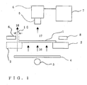
- Fig. 1 is a view of the side surface showing the configuration of an image inspection device according to a first embodiment of the invention.
- a holder stand 2 (referred to as the inspection object hold means) to hold a semiconductor wafer 1 (inspection object) that transmits infrared rays is provided on the lower side of the semiconductor wafer 1 so as to hold the semiconductor wafer 1 horizontally.
- the inspection object hold means to hold a semiconductor wafer 1 (inspection object) that transmits infrared rays is provided on the lower side of the semiconductor wafer 1 so as to hold the semiconductor wafer 1 horizontally.
- the outer shape of the semiconductor wafer 1 is a rectangle by way of example.
- An infrared light source 3 that irradiates infrared rays to an upper side is disposed below the semiconductor wafer 1, and a plate of an infrared diffusing medium 4 that diffuses infrared rays is provided above the infrared light source 3.
- the infrared diffusing medium 4 is furnished with a function of diffusing infrared rays homogeneously, and it is, for example, a translucent or frosted glass plate.
- Infrared rays after coming out from the infrared diffusing medium 4 and before going incident on the semiconductor wafer 1 are denoted by reference numeral 16 for ease of description.
- Infrared rays having passed through the semiconductor wafer 1 are denoted by reference numeral 17.
- a camera 6 (hereinafter, referred to as the infrared camera or infrared light camera) equipped with an infrared lens 5 and sensitive to infrared rays is disposed above the semiconductor wafer 1.
- a video signal imaged by the infrared camera 6 is displayed on a monitor 7, and the inspector detects a defect through a visual inspection. Alternatively, a defect is detected automatically from an image using unillustrated image processing means.
- a mask 8 (referred to as the mask means) that blocks infrared rays leaking from the outer side of the semiconductor wafer 1 is provided around the semiconductor wafer 1 at the same height.
- Fig. 2 is a view used to describe the basic configuration and operation of the holder stand (inspection object hold means) 2.
- the holder stand 2 includes four support means 2a through 2d.
- These support means have a structure such that allows each to evacuate in a direction almost parallel to the surface of the semiconductor wafer 1 up to a position not to cover the plate surface of the semiconductor wafer 1 by an unillustrated slider (referred to as the evacuater means).
- Fig. 2a is a view showing a state where none of them has evacuated.
- Fig. 2b is a view showing a state where the support stands 2b and 2d have evacuated.
- Fig. 2c is a view showing a state where the support stands 2a and 2c have evacuated.
- Infrared rays emitted from the infrared light source 3 are made homogeneous in a direction parallel to the surface of the semiconductor wafer by the infrared diffusing medium 4, and the infrared rays 16 that have been made homogeneous are irradiated to the semiconductor wafer from the back surface of the semiconductor wafer 1 (from the lower side facing the drawing).
- the semiconductor wafer 1 is positioned relatively with respect to the position of the infrared camera 6 by an unillustrated positioning mechanism and then held by the support stands 2a and 2c (referred to as the first support means) at the opposing corners as is shown in Fig. 2b.
- the support stands 2b and 2d have evacuated to positions so as not to overlap the semiconductor wafer 1.
- the irradiated infrared rays 16 pass through the inside of the semiconductor wafer to the main surface and further to the outside.
- the transmitted infrared rays 17 are captured in the infrared camera 6 by the infrared lens 5, and the monitor 7 displays an image signal outputted from the infrared camera in the form of an image that can be visually confirmed, so that an individual conducts an inspection for a crack by watching this image. It goes without saying that an inspection may be conducted automatically using an image processing device having stored unillustrated image inspection software instead of using the monitor 7. Subsequently, the support stands 2b and 2d are returned to the original positions as is shown in Fig.
- the support stands 2a and 2c are moved to evacuate to positions so as not to overlap the semiconductor wafer 1.
- the transmitted infrared rays 17 are captured in the infrared camera 6 in the same procedure as the procedure described above for an image to be displayed on the monitor 7. This enables an inspection of the image to be conducted at the portion where an inspection could not be performed last because the support stands 2a and 2c overlapped the semiconductor wafer 1.
- the mask 8 is provided while securing a slight clearance 10 for light to pass through the peripheral portion of the semiconductor wafer 1.
- the clearance 10 is large, too much light 18 passes through the clearing 10 when an image of the peripheral portion of the semiconductor wafer 1 is taken by the infrared camera 6, which gives rise to halation. It thus becomes impossible to distinguish a crack from a normal portion.
- the width of the clearance 10 is as small as 0.2 to 1.0 mm, and preferably about 0.5 mm, light 18 passing through the clearance 10 does not cause halation, and a satisfactory image can be obtained even at the peripheral portion of the semiconductor wafer 1.
- the narrower the width of the clearance becomes the less the light leaks, which causes, however, the holder stand 2 to come into contact with the semiconductor wafer 1 more frequently, and the semiconductor wafer 1 may possibly become dirty through useless contact.
- the size specified above is therefore chosen as a trade-off between leakage and contact. Consequently, it becomes possible to detect a difference in a transmission state of infrared rays between a crack and a normal portion even at the peripheral portion of the semiconductor wafer 1, which enables an inspection for a crack to be conducted across the entire surface.
- the size of the mask 8 is set so that the clearance 10 between the explanation line 99 in the drawing and the mask 8 takes a value that falls within the range specified above.
- mask means is provided so as to shield the inspection object from infrared rays while securing a clearance of 0.2 to 1.0 mm on the outer side of the angle of field when the inspection object is viewed from the infrared camera.
- a distance of the mask 8 from the inspection object 1 falls within the range of focal depth of the camera lens 5, for example, about 0.2 to 1.0 mm.
- the infrared diffusing medium 4 provided between the semiconductor wafer 1 and the infrared light source 3 enables an inspection for a crack to be conducted in a more reliable manner by making it easier to prevent halation by diffusing infrared rays. It can also protect the infrared light source 3 by preventing dirt, pieces of the semiconductor wafer 1, or the like from falling directly onto the infrared light source 3.
- a plate-shaped inspection object that transmits infrared rays is supported on the first support means.
- Infrared rays are irradiated to the inspection object from one surface thereof.
- the mask means for shielding the inspection object from the infrared rays is provided around the inspection object (it may be provided in advance).
- Infrared rays having passed through the inspection object at the portion uncovered with the first support means are imaged by the infrared camera provided on the other surface of the inspection object for an inspection to be conducted.
- the first support means is evacuated to the position so as not to shield the inspection subject.
- Infrared rays having passed through the inspection object at the portion uncovered with the second support means are imaged by the infrared camera for an inspection to be conducted.
- the imaging range in this instance includes a range that was not imaged when an image was taken while the inspection object was supported on the first support means.
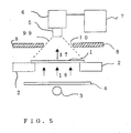
- the mask 8 is illustrated as a thick plate-shaped member.
- the end faces of the plate of the mask 8 are present at the position that can be viewed from the camera 6, light coming out from a translucent object 4 may possibly be reflected on the end faces (reflected light is denoted by 98 in the drawing) to come into the camera.
- a non-reflecting mask 80 is used herein, which is structured to have sharp edges 80a formed in a thin and sharply pointed shape as the end faces and inclined portions 80b, so that extra light will not be reflected in a direction toward the semiconductor wafer 1 and the infrared camera 6.
- the sharp edges 80a are too thin for light to be reflected, no reflected light goes into the camera.
- the inclined portions 80b prevent extra reflected light from reaching the camera. It is thus possible to obtain a more satisfactory image, which enables an inspection for a crack to be conducted in a more stable manner. It is preferable to configure in such a manner that the thickness of the sharp edges 80a at the end portion is, for example, 0.2 mm or less, or an angle of, for example, 10° to 80° is given to the inclined portions 80b with respect to the surface of the semiconductor wafer so that light reflected on the inclined portions will not go inside the semiconductor wafer 1.
- the infrared diffusing medium 4 may be provided at a specific angle, for example, an angle of 5° to 60° with respect to the horizontal level.
- a specific angle for example, an angle of 5° to 60° with respect to the horizontal level.
- the hold means 2 was described that it is moved by the unillustrated slider (evacuater means) in parallel with the surface of the semiconductor wafer 1.
- the evacuater means is not limited to the one as described above as long as it has a structure to allow the hold means 2 to evacuate to a position not to overlap the semiconductor wafer 1 (not to cover the surface of the semiconductor wafer).
- the support stands 2a through 2d may be evacuated to positions so as not to overlap the semiconductor wafer 1 by a rotation mechanism that rotates about a support point 97 as is shown in Fig. 9.
- a rotation mechanism that rotates about a support point 97 as is shown in Fig. 9.
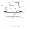
- Fig. 10 is a view showing the configuration of a fifth embodiment of the invention. Descriptions are omitted for those labeled with the same reference numerals with respect to Fig. 1 because they are the same or equivalent portions, and descriptions will be given in detail in the point that the semiconductor wafer 1 is supported on a glass plate 9 that transmits infrared rays, which is different from the first embodiment.
- the support stands 2a through 2d between the stands used to support the semiconductor wafer 1 during imaging and the stands to be evacuated during imaging.
- the support stands 2a through 2d between the stands used to support the semiconductor wafer 1 during imaging and the stands to be evacuated during imaging.
- the holding stand of Fig. 10 by configuring to support the wafer 1 using the fixed transparent (transparent for infrared rays) glass plate 9 instead of using the hold stand of Fig. 1, it is possible to inspect the semiconductor wafer 1 across the entire surface at a time. Hence, a time needed for an inspection can be shorter, and the mechanism to make the hold stand movable can be omitted. It is therefore possible to provide a more efficient and inexpensive inspection device.
- the glass plate 9 transparent for infrared rays is the light-transmitting hold means referred to in this invention.
- the mask 8 When the mask 8 is provided at the same height as the semiconductor wafer 1 as in the first embodiment, it is provided while securing a slight clearance 10 for light to pass through the peripheral portion of the semiconductor wafer 1.
- the width of the clearance 10 In a case where the width of the clearance 10 is large, too much light 18 passes through the clearing 10 when an image of the peripheral portion of the semiconductor wafer 1 is taken by the infrared camera 6, which gives rise to halation. It thus becomes impossible to distinguish a crack from a normal portion.
- the clearance 10 is as small as 0.2 to 1 mm, and preferably about 0.5 mm, light 18 passing through the clearance 10 does not cause halation, and a satisfactory image can be obtained at the peripheral portion of the semiconductor wafer 1. Consequently, it becomes possible to detect a difference in a transmission state of infrared rays between a crack and a normal portion, which enables an inspection for a crack to be conducted even at the peripheral portion of the semiconductor wafer 1.
- the mask 8 may be provided in any of the following positions: between the semiconductor wafer 1 and the infrared camera 6, almost just beside the semiconductor wafer 1, and between the semiconductor wafer 1 and the infrared light source 3. It should be noted that in a case where the mask 8 is provided between the semiconductor wafer 1 and the infrared camera 6, it is possible to avoid interference with the positioning mechanism of the semiconductor wafer and the glass plate, which in turn makes it possible to provide an inexpensive inspection device using a simpler mechanism.
- the mask 8 may be the non-reflecting mask 80 so as not to reflect extra light in a direction toward the semiconductor wafer 1 and the infrared camera 6. Reflection of light can be eliminated by providing the inclined portions to the end portions of the support stands, which in turn makes it possible to obtain a more satisfactory image. It is thus possible to conduct an inspection for a crack in a more stable manner.
- the infrared diffusing medium 4 may be provided at a specific angle.
- dirt, pieces of the semiconductor wafer, or the like will not deposit on the infrared diffusing medium 4. It is thus possible to prevent dirt, pieces, or the like from showing up in an image taken by the infrared camera. Hence, by eliminating a false recognition of a crack, it is possible to conduct an inspection for a crack in a more stable manner.
- the light-transmitting hold means 9 comes into contact with the semiconductor wafer 1. However, because the light-transmitting hold means per se is inspected together with the semiconductor wafer 1, the presence of dirt is found immediately. The light-transmitting hold means is therefore used always in a clean state, which eliminates the risk of making the semiconductor wafer dirty.
- Fig. 10 of the fifth embodiment shows a case where the glass plate 9 to hold the semiconductor wafer 1 and the infrared diffusing medium 4 that makes infrared rays homogeneous are provided separately.
- the invention is not limited to this configuration, and the infrared diffusing medium 4 may hold the semiconductor wafer 1.
- the infrared diffusing medium 4 may also serve as the glass plate 9 that supports the semiconductor wafer 1.
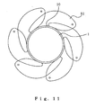
- the semiconductor wafer 1 was described and illustrated as having a rectangular shape. However, some semiconductor wafers generally manufactured are of a circular shape. Even when the semiconductor wafer is of a circular shape, the principle underlying each embedment can be applied directly. For example, it is possible to secure a clearance having the width of 0.2 to 1 mm with the use of a mask having the structure similar to that of the mechanical aperture mechanism in a camera like an aperture mask 81 shown in Fig. 11. More specifically, it is configured in such a manner that plural infrared shielding blades are provided to overlap one on another in a rotatable manner respectively around plural rotational shafts disposed on a circle, and the diameter of the hole at the center can be varied by changing the angel of rotation.
- the shape of such a mechanical aperture mechanism is well known, and detailed description thereof is omitted herein. It goes without saying, however, that the aperture mechanism mask is usable for a circular inspection object in all the embodiments described above.
- the inspection object was described as the semiconductor wafer 1. However, it is not limited to a semiconductor wafer as long as it is an inspection object that transmits infrared rays. It goes without saying that an inspection can be conducted, for example, for a liquid crystal panel or the front panel of a solar battery.
- the image inspection device of the invention can be used not only for an inspection of a semiconductor wafer, but also for an inspection of a panel plate of a liquid crystal display and a solar battery panel.
Landscapes
- Physics & Mathematics (AREA)
- Health & Medical Sciences (AREA)
- Life Sciences & Earth Sciences (AREA)
- Chemical & Material Sciences (AREA)
- Analytical Chemistry (AREA)
- Biochemistry (AREA)
- General Health & Medical Sciences (AREA)
- General Physics & Mathematics (AREA)
- Immunology (AREA)
- Pathology (AREA)
- Investigating Materials By The Use Of Optical Means Adapted For Particular Applications (AREA)
- Testing Or Measuring Of Semiconductors Or The Like (AREA)
- Testing Of Optical Devices Or Fibers (AREA)
- Testing, Inspecting, Measuring Of Stereoscopic Televisions And Televisions (AREA)
- Measuring And Recording Apparatus For Diagnosis (AREA)
- Transforming Light Signals Into Electric Signals (AREA)
Applications Claiming Priority (1)
| Application Number | Priority Date | Filing Date | Title |
|---|---|---|---|
| JP2006129218A JP4878907B2 (ja) | 2006-05-08 | 2006-05-08 | 画像検査装置およびこの画像検査装置を用いた画像検査方法 |
Publications (3)
| Publication Number | Publication Date |
|---|---|
| EP1855103A2 true EP1855103A2 (de) | 2007-11-14 |
| EP1855103A3 EP1855103A3 (de) | 2009-12-23 |
| EP1855103B1 EP1855103B1 (de) | 2015-10-21 |
Family
ID=38293983
Family Applications (1)
| Application Number | Title | Priority Date | Filing Date |
|---|---|---|---|
| EP07008985.9A Not-in-force EP1855103B1 (de) | 2006-05-08 | 2007-05-03 | Bildprüfvorrichtung und die Bildprüfvorrichtung verwendendes Bildprüfverfahren |
Country Status (5)
| Country | Link |
|---|---|
| US (1) | US7569822B2 (de) |
| EP (1) | EP1855103B1 (de) |
| JP (1) | JP4878907B2 (de) |
| CN (1) | CN100590427C (de) |
| NO (1) | NO338042B1 (de) |
Cited By (2)
| Publication number | Priority date | Publication date | Assignee | Title |
|---|---|---|---|---|
| DE202013009329U1 (de) | 2013-10-18 | 2014-03-14 | Institut für innovative Technologien, Technologietransfer, Ausbildung und berufsbegleitende Weiterbildung (ITW) e.V. | Hochleistungs-Flächenlichtquelle |
| DE102013017501A1 (de) | 2013-10-18 | 2015-04-23 | Institut für innovative Technologien, Technologietransfer, Ausbildung und berufsbegleitende Weiterbildung (ITW) e. V. | Verfahren und Vorrichtung zur Prüfung von Siliziumbauteilen |
Families Citing this family (27)
| Publication number | Priority date | Publication date | Assignee | Title |
|---|---|---|---|---|
| JP5128920B2 (ja) | 2007-12-03 | 2013-01-23 | 芝浦メカトロニクス株式会社 | 基板表面検査装置及び基板表面検査方法 |
| KR101001113B1 (ko) | 2008-11-12 | 2010-12-14 | 주식회사 코로 | 웨이퍼 결함의 검사장치 및 검사방법 |
| KR20110055787A (ko) * | 2009-11-20 | 2011-05-26 | 재단법인 서울테크노파크 | 레이저를 이용한 접합웨이퍼 검사장치 |
| KR101115010B1 (ko) * | 2010-07-13 | 2012-03-06 | 한미반도체 주식회사 | 웨이퍼 검사 장치 |
| CN103250047A (zh) * | 2010-12-09 | 2013-08-14 | 旭硝子株式会社 | 玻璃带内缺陷测定方法和玻璃带内缺陷测定系统 |
| WO2013002179A1 (ja) * | 2011-06-27 | 2013-01-03 | 株式会社ニコン | パターンの評価方法、パターン評価装置、および半導体装置の製造方法 |
| JP5323906B2 (ja) * | 2011-09-12 | 2013-10-23 | シャープ株式会社 | 配線欠陥検出方法および配線欠陥検出装置 |
| JP5753516B2 (ja) * | 2011-11-28 | 2015-07-22 | 東京エレクトロン株式会社 | 基板撮像装置及び基板撮像方法 |
| JP5966704B2 (ja) * | 2012-07-11 | 2016-08-10 | 株式会社島津製作所 | 基板検査装置および基板検査装置用透過照明装置 |
| JP5900628B2 (ja) * | 2012-09-05 | 2016-04-06 | 株式会社島津製作所 | 太陽電池セルの検査装置 |
| JP2014154708A (ja) * | 2013-02-08 | 2014-08-25 | Disco Abrasive Syst Ltd | ウエーハの割れ検出方法及びウエーハの割れ検出装置 |
| TW201511152A (zh) * | 2013-09-09 | 2015-03-16 | Cheng Mei Instr Technology Co Ltd | 線性掃瞄總成 |
| CN103604815B (zh) * | 2013-11-26 | 2016-01-13 | 上海海事大学 | 玻璃晶片检测装置与标定方法 |
| MY185911A (en) * | 2014-12-05 | 2021-06-14 | Kla Tencor Corp | Apparatus, method and computer program product for defect detection in work pieces |
| JP6658051B2 (ja) * | 2016-02-16 | 2020-03-04 | 三菱電機株式会社 | ウエハの検査装置、ウエハの検査方法および半導体装置の製造方法 |
| US10692204B2 (en) | 2016-08-01 | 2020-06-23 | The Boeing Company | System and method for high speed surface and subsurface FOD and defect detection |
| JP6975551B2 (ja) * | 2017-05-18 | 2021-12-01 | ファスフォードテクノロジ株式会社 | 半導体製造装置および半導体装置の製造方法 |
| US10596319B2 (en) | 2017-11-23 | 2020-03-24 | Aesynt Incorporated | Compounding device system |
| US10991264B2 (en) * | 2017-11-23 | 2021-04-27 | Omnicell, Inc. | Multi-camera imaging for IV compounding |
| US11335444B2 (en) | 2017-11-30 | 2022-05-17 | Omnicell, Inc. | IV compounding systems and methods |
| US20190257876A1 (en) * | 2018-02-21 | 2019-08-22 | Asm Technology Singapore Pte Ltd | System and method for detecting defects in an electronic device |
| JP7102271B2 (ja) * | 2018-07-17 | 2022-07-19 | ファスフォードテクノロジ株式会社 | 半導体製造装置および半導体装置の製造方法 |
| CN109596640B (zh) * | 2018-12-05 | 2021-09-03 | 京东方科技集团股份有限公司 | 异物检测方法及装置 |
| JP2021067587A (ja) * | 2019-10-25 | 2021-04-30 | 日本電産サンキョー株式会社 | 外観検査装置 |
| CN111122654B (zh) * | 2020-01-14 | 2022-08-12 | 国宏华业投资有限公司 | 一种晶体表面缺陷的双面红外热像检测系统 |
| TWI884618B (zh) * | 2023-12-06 | 2025-05-21 | 晶呈科技股份有限公司 | 晶圓缺陷分析裝置及晶圓缺陷分析方法 |
| TWI891276B (zh) * | 2024-03-08 | 2025-07-21 | 由田新技股份有限公司 | 晶圓吸附載台、晶圓檢測裝置、以及晶圓檢測方法 |
Citations (1)
| Publication number | Priority date | Publication date | Assignee | Title |
|---|---|---|---|---|
| JPH08220008A (ja) | 1995-02-15 | 1996-08-30 | Mitsubishi Electric Corp | 赤外検査装置 |
Family Cites Families (10)
| Publication number | Priority date | Publication date | Assignee | Title |
|---|---|---|---|---|
| JPH01120652A (ja) * | 1987-11-04 | 1989-05-12 | Nec Corp | 入出力装置監視時間設定方式 |
| KR100606460B1 (ko) * | 1997-07-17 | 2006-07-31 | 호야 가부시키가이샤 | 투광성물질의 불균일성검사방법 및 그 장치와 투명기판의 선별방법 |
| US6236044B1 (en) | 1998-08-21 | 2001-05-22 | Trw Inc. | Method and apparatus for inspection of a substrate by use of a ring illuminator |
| AU2002219847A1 (en) * | 2000-11-15 | 2002-05-27 | Real Time Metrology, Inc. | Optical method and apparatus for inspecting large area planar objects |
| JP2002214158A (ja) * | 2001-01-19 | 2002-07-31 | Central Glass Co Ltd | 透明板状体の欠点検出方法および検出装置 |
| JP2002340794A (ja) * | 2001-05-15 | 2002-11-27 | Sumitomo Mitsubishi Silicon Corp | 半導体ウェーハの赤外吸収測定法 |
| US6654109B2 (en) * | 2002-02-05 | 2003-11-25 | Taiwan Semiconductor Manufacturing Co. Ltd | System for detecting surface defects in semiconductor wafers |
| JP3948439B2 (ja) * | 2003-07-08 | 2007-07-25 | 三菱電機株式会社 | 密着イメージセンサおよびこれを用いた画像読み取り装置 |
| DE102004015326A1 (de) * | 2004-03-30 | 2005-10-20 | Leica Microsystems | Vorrichtung und Verfahren zur Inspektion eines Halbleiterbauteils |
| DE102004029212B4 (de) * | 2004-06-16 | 2006-07-13 | Leica Microsystems Semiconductor Gmbh | Vorrichtung und Verfahren zur optischen Auf- und/oder Durchlichtinspektion von Mikrostrukturen im IR |
-
2006
- 2006-05-08 JP JP2006129218A patent/JP4878907B2/ja not_active Expired - Fee Related
-
2007
- 2007-04-17 US US11/785,408 patent/US7569822B2/en not_active Expired - Fee Related
- 2007-04-23 NO NO20072102A patent/NO338042B1/no not_active IP Right Cessation
- 2007-04-29 CN CN200710101136A patent/CN100590427C/zh not_active Expired - Fee Related
- 2007-05-03 EP EP07008985.9A patent/EP1855103B1/de not_active Not-in-force
Patent Citations (1)
| Publication number | Priority date | Publication date | Assignee | Title |
|---|---|---|---|---|
| JPH08220008A (ja) | 1995-02-15 | 1996-08-30 | Mitsubishi Electric Corp | 赤外検査装置 |
Cited By (2)
| Publication number | Priority date | Publication date | Assignee | Title |
|---|---|---|---|---|
| DE202013009329U1 (de) | 2013-10-18 | 2014-03-14 | Institut für innovative Technologien, Technologietransfer, Ausbildung und berufsbegleitende Weiterbildung (ITW) e.V. | Hochleistungs-Flächenlichtquelle |
| DE102013017501A1 (de) | 2013-10-18 | 2015-04-23 | Institut für innovative Technologien, Technologietransfer, Ausbildung und berufsbegleitende Weiterbildung (ITW) e. V. | Verfahren und Vorrichtung zur Prüfung von Siliziumbauteilen |
Also Published As
| Publication number | Publication date |
|---|---|
| CN100590427C (zh) | 2010-02-17 |
| JP2007303829A (ja) | 2007-11-22 |
| NO338042B1 (no) | 2016-07-25 |
| US7569822B2 (en) | 2009-08-04 |
| EP1855103A3 (de) | 2009-12-23 |
| JP4878907B2 (ja) | 2012-02-15 |
| US20070257192A1 (en) | 2007-11-08 |
| CN101071107A (zh) | 2007-11-14 |
| EP1855103B1 (de) | 2015-10-21 |
| NO20072102L (no) | 2007-11-09 |
Similar Documents
| Publication | Publication Date | Title |
|---|---|---|
| EP1855103B1 (de) | Bildprüfvorrichtung und die Bildprüfvorrichtung verwendendes Bildprüfverfahren | |
| TWI663394B (zh) | 在工作件中用於缺陷偵測的裝置,方法及電腦程式產品 | |
| JP5144401B2 (ja) | ウエハ用検査装置 | |
| TWI442016B (zh) | A light source for illumination and a pattern inspection device using it | |
| JPS58219441A (ja) | 凸面体の表面欠陥検査装置 | |
| JP2014029336A (ja) | 観察装置および観察方法 | |
| JP4847128B2 (ja) | 表面欠陥検査装置 | |
| KR101151274B1 (ko) | 결점 검사장치 | |
| JPH1062354A (ja) | 透明板の欠陥検査装置及び欠陥検査方法 | |
| JP2009103494A (ja) | 表面検査装置 | |
| TW200925588A (en) | Defect inspecting device and its method thereof | |
| JP2005241586A (ja) | 光学フィルムの検査装置および光学フィルムの検査方法 | |
| JP4429177B2 (ja) | 透明容器の欠陥検査方法及び装置 | |
| JP2821460B2 (ja) | 透明基板の傷検査装置 | |
| JP2004257776A (ja) | 光透過体検査装置 | |
| JP2008064656A (ja) | 周縁検査装置 | |
| JP2002014058A (ja) | 検査方法及び装置 | |
| JP4855193B2 (ja) | 薄板検査装置 | |
| JPH09218162A (ja) | 表面欠陥検査装置 | |
| JP2009222629A (ja) | 被検物端面検査装置 | |
| JP2012198071A (ja) | 光学ガラス検査装置および検査方法 | |
| JP3360795B2 (ja) | 光学部材検査装置 | |
| JP2007010640A (ja) | 表面欠陥検査装置 | |
| JP4886315B2 (ja) | 撮像システムおよび光学部材検査装置 | |
| JP2000019060A (ja) | 光学部材検査装置 |
Legal Events
| Date | Code | Title | Description |
|---|---|---|---|
| PUAI | Public reference made under article 153(3) epc to a published international application that has entered the european phase |
Free format text: ORIGINAL CODE: 0009012 |
|
| AK | Designated contracting states |
Kind code of ref document: A2 Designated state(s): AT BE BG CH CY CZ DE DK EE ES FI FR GB GR HU IE IS IT LI LT LU LV MC MT NL PL PT RO SE SI SK TR |
|
| AX | Request for extension of the european patent |
Extension state: AL BA HR MK YU |
|
| PUAL | Search report despatched |
Free format text: ORIGINAL CODE: 0009013 |
|
| AK | Designated contracting states |
Kind code of ref document: A3 Designated state(s): AT BE BG CH CY CZ DE DK EE ES FI FR GB GR HU IE IS IT LI LT LU LV MC MT NL PL PT RO SE SI SK TR |
|
| AX | Request for extension of the european patent |
Extension state: AL BA HR MK RS |
|
| 17P | Request for examination filed |
Effective date: 20100126 |
|
| 17Q | First examination report despatched |
Effective date: 20100224 |
|
| AKX | Designation fees paid |
Designated state(s): DE FR |
|
| GRAP | Despatch of communication of intention to grant a patent |
Free format text: ORIGINAL CODE: EPIDOSNIGR1 |
|
| INTG | Intention to grant announced |
Effective date: 20150507 |
|
| GRAS | Grant fee paid |
Free format text: ORIGINAL CODE: EPIDOSNIGR3 |
|
| GRAA | (expected) grant |
Free format text: ORIGINAL CODE: 0009210 |
|
| AK | Designated contracting states |
Kind code of ref document: B1 Designated state(s): DE FR |
|
| REG | Reference to a national code |
Ref country code: DE Ref legal event code: R096 Ref document number: 602007043546 Country of ref document: DE |
|
| REG | Reference to a national code |
Ref country code: DE Ref legal event code: R097 Ref document number: 602007043546 Country of ref document: DE |
|
| PLBE | No opposition filed within time limit |
Free format text: ORIGINAL CODE: 0009261 |
|
| STAA | Information on the status of an ep patent application or granted ep patent |
Free format text: STATUS: NO OPPOSITION FILED WITHIN TIME LIMIT |
|
| 26N | No opposition filed |
Effective date: 20160722 |
|
| REG | Reference to a national code |
Ref country code: FR Ref legal event code: ST Effective date: 20170131 |
|
| PG25 | Lapsed in a contracting state [announced via postgrant information from national office to epo] |
Ref country code: FR Free format text: LAPSE BECAUSE OF NON-PAYMENT OF DUE FEES Effective date: 20160531 |
|
| REG | Reference to a national code |
Ref country code: DE Ref legal event code: R084 Ref document number: 602007043546 Country of ref document: DE |
|
| PGFP | Annual fee paid to national office [announced via postgrant information from national office to epo] |
Ref country code: DE Payment date: 20180417 Year of fee payment: 12 |
|
| REG | Reference to a national code |
Ref country code: DE Ref legal event code: R119 Ref document number: 602007043546 Country of ref document: DE |
|
| PG25 | Lapsed in a contracting state [announced via postgrant information from national office to epo] |
Ref country code: DE Free format text: LAPSE BECAUSE OF NON-PAYMENT OF DUE FEES Effective date: 20191203 |