EP1855321A2 - Photonentransparentes Fenster mit niedrigem spezifischem Widerstand an einem lichtempfindlichen Siliciumdetektor - Google Patents
Photonentransparentes Fenster mit niedrigem spezifischem Widerstand an einem lichtempfindlichen Siliciumdetektor Download PDFInfo
- Publication number
- EP1855321A2 EP1855321A2 EP07016419A EP07016419A EP1855321A2 EP 1855321 A2 EP1855321 A2 EP 1855321A2 EP 07016419 A EP07016419 A EP 07016419A EP 07016419 A EP07016419 A EP 07016419A EP 1855321 A2 EP1855321 A2 EP 1855321A2
- Authority
- EP
- European Patent Office
- Prior art keywords
- substrate
- backside
- ccd
- silicon
- photon
- Prior art date
- Legal status (The legal status is an assumption and is not a legal conclusion. Google has not performed a legal analysis and makes no representation as to the accuracy of the status listed.)
- Withdrawn
Links
- XUIMIQQOPSSXEZ-UHFFFAOYSA-N Silicon Chemical compound [Si] XUIMIQQOPSSXEZ-UHFFFAOYSA-N 0.000 title claims abstract description 140
- 229910052710 silicon Inorganic materials 0.000 title claims abstract description 138
- 239000010703 silicon Substances 0.000 title claims abstract description 138
- 239000002800 charge carrier Substances 0.000 claims abstract description 16
- 239000000758 substrate Substances 0.000 claims description 152
- 229910021420 polycrystalline silicon Inorganic materials 0.000 claims description 64
- 238000000576 coating method Methods 0.000 claims description 18
- 238000010521 absorption reaction Methods 0.000 claims description 14
- 239000011248 coating agent Substances 0.000 claims description 12
- 238000001514 detection method Methods 0.000 claims description 11
- OAICVXFJPJFONN-UHFFFAOYSA-N Phosphorus Chemical compound [P] OAICVXFJPJFONN-UHFFFAOYSA-N 0.000 claims description 5
- 229910052698 phosphorus Inorganic materials 0.000 claims description 5
- 239000011574 phosphorus Substances 0.000 claims description 5
- 230000005670 electromagnetic radiation Effects 0.000 claims description 4
- 230000000779 depleting effect Effects 0.000 claims description 2
- 238000012546 transfer Methods 0.000 claims description 2
- 230000005855 radiation Effects 0.000 abstract description 12
- 235000012431 wafers Nutrition 0.000 description 135
- 239000010410 layer Substances 0.000 description 131
- 229920005591 polysilicon Polymers 0.000 description 58
- 238000000151 deposition Methods 0.000 description 44
- 230000008021 deposition Effects 0.000 description 42
- 239000007943 implant Substances 0.000 description 28
- 229920002120 photoresistant polymer Polymers 0.000 description 28
- 238000000034 method Methods 0.000 description 27
- XLYOFNOQVPJJNP-UHFFFAOYSA-N water Chemical compound O XLYOFNOQVPJJNP-UHFFFAOYSA-N 0.000 description 27
- 150000004767 nitrides Chemical class 0.000 description 23
- 241000252506 Characiformes Species 0.000 description 22
- FFUAGWLWBBFQJT-UHFFFAOYSA-N hexamethyldisilazane Chemical compound C[Si](C)(C)N[Si](C)(C)C FFUAGWLWBBFQJT-UHFFFAOYSA-N 0.000 description 22
- 230000003647 oxidation Effects 0.000 description 22
- 238000007254 oxidation reaction Methods 0.000 description 22
- 239000006117 anti-reflective coating Substances 0.000 description 15
- BHEPBYXIRTUNPN-UHFFFAOYSA-N hydridophosphorus(.) (triplet) Chemical compound [PH] BHEPBYXIRTUNPN-UHFFFAOYSA-N 0.000 description 15
- VYPSYNLAJGMNEJ-UHFFFAOYSA-N Silicium dioxide Chemical compound O=[Si]=O VYPSYNLAJGMNEJ-UHFFFAOYSA-N 0.000 description 14
- 238000004518 low pressure chemical vapour deposition Methods 0.000 description 14
- 239000000463 material Substances 0.000 description 11
- 230000015556 catabolic process Effects 0.000 description 10
- 238000009792 diffusion process Methods 0.000 description 10
- 230000008901 benefit Effects 0.000 description 9
- 238000004519 manufacturing process Methods 0.000 description 9
- 230000008569 process Effects 0.000 description 9
- 239000000969 carrier Substances 0.000 description 8
- 230000004044 response Effects 0.000 description 8
- QVGXLLKOCUKJST-UHFFFAOYSA-N atomic oxygen Chemical compound [O] QVGXLLKOCUKJST-UHFFFAOYSA-N 0.000 description 7
- 238000005286 illumination Methods 0.000 description 7
- AMGQUBHHOARCQH-UHFFFAOYSA-N indium;oxotin Chemical compound [In].[Sn]=O AMGQUBHHOARCQH-UHFFFAOYSA-N 0.000 description 7
- 238000005259 measurement Methods 0.000 description 7
- 229910052751 metal Inorganic materials 0.000 description 7
- 239000002184 metal Substances 0.000 description 7
- 239000001301 oxygen Substances 0.000 description 7
- 229910052760 oxygen Inorganic materials 0.000 description 7
- 239000000377 silicon dioxide Substances 0.000 description 7
- 238000002834 transmittance Methods 0.000 description 7
- ZOXJGFHDIHLPTG-UHFFFAOYSA-N Boron Chemical compound [B] ZOXJGFHDIHLPTG-UHFFFAOYSA-N 0.000 description 6
- BLRPTPMANUNPDV-UHFFFAOYSA-N Silane Chemical compound [SiH4] BLRPTPMANUNPDV-UHFFFAOYSA-N 0.000 description 6
- 229910052782 aluminium Inorganic materials 0.000 description 6
- XAGFODPZIPBFFR-UHFFFAOYSA-N aluminium Chemical compound [Al] XAGFODPZIPBFFR-UHFFFAOYSA-N 0.000 description 6
- 229910052796 boron Inorganic materials 0.000 description 6
- 230000005684 electric field Effects 0.000 description 6
- 230000003287 optical effect Effects 0.000 description 6
- 238000012360 testing method Methods 0.000 description 6
- 238000011161 development Methods 0.000 description 5
- 230000000694 effects Effects 0.000 description 5
- 239000007789 gas Substances 0.000 description 5
- 238000005247 gettering Methods 0.000 description 5
- 238000011065 in-situ storage Methods 0.000 description 5
- NBIIXXVUZAFLBC-UHFFFAOYSA-N Phosphoric acid Chemical compound OP(O)(O)=O NBIIXXVUZAFLBC-UHFFFAOYSA-N 0.000 description 4
- 229910052581 Si3N4 Inorganic materials 0.000 description 4
- 238000000137 annealing Methods 0.000 description 4
- 238000003491 array Methods 0.000 description 4
- 230000007423 decrease Effects 0.000 description 4
- 239000002019 doping agent Substances 0.000 description 4
- 230000005661 hydrophobic surface Effects 0.000 description 4
- 238000002310 reflectometry Methods 0.000 description 4
- 239000000523 sample Substances 0.000 description 4
- 230000035945 sensitivity Effects 0.000 description 4
- 229910000077 silane Inorganic materials 0.000 description 4
- 235000012239 silicon dioxide Nutrition 0.000 description 4
- HQVNEWCFYHHQES-UHFFFAOYSA-N silicon nitride Chemical compound N12[Si]34N5[Si]62N3[Si]51N64 HQVNEWCFYHHQES-UHFFFAOYSA-N 0.000 description 4
- 238000003892 spreading Methods 0.000 description 4
- 230000007480 spreading Effects 0.000 description 4
- 238000009736 wetting Methods 0.000 description 4
- 101100269850 Caenorhabditis elegans mask-1 gene Proteins 0.000 description 3
- 229920004482 WACKER® Polymers 0.000 description 3
- 230000004888 barrier function Effects 0.000 description 3
- 238000005229 chemical vapour deposition Methods 0.000 description 3
- 229910052681 coesite Inorganic materials 0.000 description 3
- PMHQVHHXPFUNSP-UHFFFAOYSA-M copper(1+);methylsulfanylmethane;bromide Chemical compound Br[Cu].CSC PMHQVHHXPFUNSP-UHFFFAOYSA-M 0.000 description 3
- 229910052906 cristobalite Inorganic materials 0.000 description 3
- 230000003247 decreasing effect Effects 0.000 description 3
- 239000000203 mixture Substances 0.000 description 3
- 230000009467 reduction Effects 0.000 description 3
- 238000004088 simulation Methods 0.000 description 3
- 229910052682 stishovite Inorganic materials 0.000 description 3
- 229910052905 tridymite Inorganic materials 0.000 description 3
- 238000009279 wet oxidation reaction Methods 0.000 description 3
- IJGRMHOSHXDMSA-UHFFFAOYSA-N Atomic nitrogen Chemical compound N#N IJGRMHOSHXDMSA-UHFFFAOYSA-N 0.000 description 2
- XYFCBTPGUUZFHI-UHFFFAOYSA-N Phosphine Chemical compound P XYFCBTPGUUZFHI-UHFFFAOYSA-N 0.000 description 2
- 229910000147 aluminium phosphate Inorganic materials 0.000 description 2
- 230000003667 anti-reflective effect Effects 0.000 description 2
- 238000013461 design Methods 0.000 description 2
- 238000009826 distribution Methods 0.000 description 2
- 238000005516 engineering process Methods 0.000 description 2
- 238000005530 etching Methods 0.000 description 2
- 238000011049 filling Methods 0.000 description 2
- 229910000449 hafnium oxide Inorganic materials 0.000 description 2
- WIHZLLGSGQNAGK-UHFFFAOYSA-N hafnium(4+);oxygen(2-) Chemical compound [O-2].[O-2].[Hf+4] WIHZLLGSGQNAGK-UHFFFAOYSA-N 0.000 description 2
- 238000010438 heat treatment Methods 0.000 description 2
- 238000003384 imaging method Methods 0.000 description 2
- 239000012535 impurity Substances 0.000 description 2
- 239000012212 insulator Substances 0.000 description 2
- 238000005468 ion implantation Methods 0.000 description 2
- 238000002955 isolation Methods 0.000 description 2
- 229910000464 lead oxide Inorganic materials 0.000 description 2
- BOYZAERJCXIRAX-UHFFFAOYSA-N lutetium(3+);trisilicate Chemical compound [Lu+3].[Lu+3].[Lu+3].[Lu+3].[O-][Si]([O-])([O-])[O-].[O-][Si]([O-])([O-])[O-].[O-][Si]([O-])([O-])[O-] BOYZAERJCXIRAX-UHFFFAOYSA-N 0.000 description 2
- ORUIBWPALBXDOA-UHFFFAOYSA-L magnesium fluoride Chemical compound [F-].[F-].[Mg+2] ORUIBWPALBXDOA-UHFFFAOYSA-L 0.000 description 2
- 229910001635 magnesium fluoride Inorganic materials 0.000 description 2
- TWNQGVIAIRXVLR-UHFFFAOYSA-N oxo(oxoalumanyloxy)alumane Chemical compound O=[Al]O[Al]=O TWNQGVIAIRXVLR-UHFFFAOYSA-N 0.000 description 2
- YEXPOXQUZXUXJW-UHFFFAOYSA-N oxolead Chemical compound [Pb]=O YEXPOXQUZXUXJW-UHFFFAOYSA-N 0.000 description 2
- 238000012545 processing Methods 0.000 description 2
- 238000011160 research Methods 0.000 description 2
- 239000007858 starting material Substances 0.000 description 2
- XOLBLPGZBRYERU-UHFFFAOYSA-N tin dioxide Chemical compound O=[Sn]=O XOLBLPGZBRYERU-UHFFFAOYSA-N 0.000 description 2
- 229910052721 tungsten Inorganic materials 0.000 description 2
- 239000010937 tungsten Substances 0.000 description 2
- XKRFYHLGVUSROY-UHFFFAOYSA-N Argon Chemical group [Ar] XKRFYHLGVUSROY-UHFFFAOYSA-N 0.000 description 1
- 230000005355 Hall effect Effects 0.000 description 1
- 238000013459 approach Methods 0.000 description 1
- 230000005540 biological transmission Effects 0.000 description 1
- 229910052797 bismuth Inorganic materials 0.000 description 1
- JCXGWMGPZLAOME-UHFFFAOYSA-N bismuth atom Chemical compound [Bi] JCXGWMGPZLAOME-UHFFFAOYSA-N 0.000 description 1
- 239000005380 borophosphosilicate glass Substances 0.000 description 1
- 238000012512 characterization method Methods 0.000 description 1
- 239000004020 conductor Substances 0.000 description 1
- 239000000356 contaminant Substances 0.000 description 1
- 238000005336 cracking Methods 0.000 description 1
- 239000013078 crystal Substances 0.000 description 1
- 230000001419 dependent effect Effects 0.000 description 1
- 238000002474 experimental method Methods 0.000 description 1
- 229910052736 halogen Inorganic materials 0.000 description 1
- 230000006872 improvement Effects 0.000 description 1
- RHZWSUVWRRXEJF-UHFFFAOYSA-N indium tin Chemical compound [In].[Sn] RHZWSUVWRRXEJF-UHFFFAOYSA-N 0.000 description 1
- PJXISJQVUVHSOJ-UHFFFAOYSA-N indium(III) oxide Inorganic materials [O-2].[O-2].[O-2].[In+3].[In+3] PJXISJQVUVHSOJ-UHFFFAOYSA-N 0.000 description 1
- 239000011810 insulating material Substances 0.000 description 1
- 150000002500 ions Chemical class 0.000 description 1
- 230000031700 light absorption Effects 0.000 description 1
- 238000001755 magnetron sputter deposition Methods 0.000 description 1
- 238000012986 modification Methods 0.000 description 1
- 230000004048 modification Effects 0.000 description 1
- 238000001451 molecular beam epitaxy Methods 0.000 description 1
- 229910052757 nitrogen Inorganic materials 0.000 description 1
- 239000013307 optical fiber Substances 0.000 description 1
- 229910000073 phosphorus hydride Inorganic materials 0.000 description 1
- 238000002600 positron emission tomography Methods 0.000 description 1
- 238000005036 potential barrier Methods 0.000 description 1
- 238000005546 reactive sputtering Methods 0.000 description 1
- 239000004065 semiconductor Substances 0.000 description 1
- 230000003595 spectral effect Effects 0.000 description 1
- 238000001228 spectrum Methods 0.000 description 1
- 239000002344 surface layer Substances 0.000 description 1
- 238000005382 thermal cycling Methods 0.000 description 1
- 229910001887 tin oxide Inorganic materials 0.000 description 1
- WFKWXMTUELFFGS-UHFFFAOYSA-N tungsten Chemical compound [W] WFKWXMTUELFFGS-UHFFFAOYSA-N 0.000 description 1
- -1 tungsten halogen Chemical class 0.000 description 1
Images




Classifications
-
- H—ELECTRICITY
- H10—SEMICONDUCTOR DEVICES; ELECTRIC SOLID-STATE DEVICES NOT OTHERWISE PROVIDED FOR
- H10F—INORGANIC SEMICONDUCTOR DEVICES SENSITIVE TO INFRARED RADIATION, LIGHT, ELECTROMAGNETIC RADIATION OF SHORTER WAVELENGTH OR CORPUSCULAR RADIATION
- H10F39/00—Integrated devices, or assemblies of multiple devices, comprising at least one element covered by group H10F30/00, e.g. radiation detectors comprising photodiode arrays
- H10F39/80—Constructional details of image sensors
- H10F39/807—Pixel isolation structures
-
- H—ELECTRICITY
- H10—SEMICONDUCTOR DEVICES; ELECTRIC SOLID-STATE DEVICES NOT OTHERWISE PROVIDED FOR
- H10F—INORGANIC SEMICONDUCTOR DEVICES SENSITIVE TO INFRARED RADIATION, LIGHT, ELECTROMAGNETIC RADIATION OF SHORTER WAVELENGTH OR CORPUSCULAR RADIATION
- H10F39/00—Integrated devices, or assemblies of multiple devices, comprising at least one element covered by group H10F30/00, e.g. radiation detectors comprising photodiode arrays
- H10F39/011—Manufacture or treatment of image sensors covered by group H10F39/12
- H10F39/024—Manufacture or treatment of image sensors covered by group H10F39/12 of coatings or optical elements
-
- H—ELECTRICITY
- H10—SEMICONDUCTOR DEVICES; ELECTRIC SOLID-STATE DEVICES NOT OTHERWISE PROVIDED FOR
- H10F—INORGANIC SEMICONDUCTOR DEVICES SENSITIVE TO INFRARED RADIATION, LIGHT, ELECTROMAGNETIC RADIATION OF SHORTER WAVELENGTH OR CORPUSCULAR RADIATION
- H10F39/00—Integrated devices, or assemblies of multiple devices, comprising at least one element covered by group H10F30/00, e.g. radiation detectors comprising photodiode arrays
- H10F39/10—Integrated devices
- H10F39/12—Image sensors
- H10F39/15—Charge-coupled device [CCD] image sensors
-
- H—ELECTRICITY
- H10—SEMICONDUCTOR DEVICES; ELECTRIC SOLID-STATE DEVICES NOT OTHERWISE PROVIDED FOR
- H10F—INORGANIC SEMICONDUCTOR DEVICES SENSITIVE TO INFRARED RADIATION, LIGHT, ELECTROMAGNETIC RADIATION OF SHORTER WAVELENGTH OR CORPUSCULAR RADIATION
- H10F39/00—Integrated devices, or assemblies of multiple devices, comprising at least one element covered by group H10F30/00, e.g. radiation detectors comprising photodiode arrays
- H10F39/10—Integrated devices
- H10F39/12—Image sensors
- H10F39/15—Charge-coupled device [CCD] image sensors
- H10F39/151—Geometry or disposition of pixel elements, address lines or gate electrodes
-
- H—ELECTRICITY
- H10—SEMICONDUCTOR DEVICES; ELECTRIC SOLID-STATE DEVICES NOT OTHERWISE PROVIDED FOR
- H10F—INORGANIC SEMICONDUCTOR DEVICES SENSITIVE TO INFRARED RADIATION, LIGHT, ELECTROMAGNETIC RADIATION OF SHORTER WAVELENGTH OR CORPUSCULAR RADIATION
- H10F39/00—Integrated devices, or assemblies of multiple devices, comprising at least one element covered by group H10F30/00, e.g. radiation detectors comprising photodiode arrays
- H10F39/10—Integrated devices
- H10F39/12—Image sensors
- H10F39/199—Back-illuminated image sensors
-
- H—ELECTRICITY
- H10—SEMICONDUCTOR DEVICES; ELECTRIC SOLID-STATE DEVICES NOT OTHERWISE PROVIDED FOR
- H10F—INORGANIC SEMICONDUCTOR DEVICES SENSITIVE TO INFRARED RADIATION, LIGHT, ELECTROMAGNETIC RADIATION OF SHORTER WAVELENGTH OR CORPUSCULAR RADIATION
- H10F39/00—Integrated devices, or assemblies of multiple devices, comprising at least one element covered by group H10F30/00, e.g. radiation detectors comprising photodiode arrays
- H10F39/80—Constructional details of image sensors
-
- H—ELECTRICITY
- H10—SEMICONDUCTOR DEVICES; ELECTRIC SOLID-STATE DEVICES NOT OTHERWISE PROVIDED FOR
- H10F—INORGANIC SEMICONDUCTOR DEVICES SENSITIVE TO INFRARED RADIATION, LIGHT, ELECTROMAGNETIC RADIATION OF SHORTER WAVELENGTH OR CORPUSCULAR RADIATION
- H10F77/00—Constructional details of devices covered by this subclass
- H10F77/20—Electrodes
- H10F77/244—Electrodes made of transparent conductive layers, e.g. transparent conductive oxide [TCO] layers
-
- H—ELECTRICITY
- H10—SEMICONDUCTOR DEVICES; ELECTRIC SOLID-STATE DEVICES NOT OTHERWISE PROVIDED FOR
- H10F—INORGANIC SEMICONDUCTOR DEVICES SENSITIVE TO INFRARED RADIATION, LIGHT, ELECTROMAGNETIC RADIATION OF SHORTER WAVELENGTH OR CORPUSCULAR RADIATION
- H10F77/00—Constructional details of devices covered by this subclass
- H10F77/20—Electrodes
- H10F77/244—Electrodes made of transparent conductive layers, e.g. transparent conductive oxide [TCO] layers
- H10F77/247—Electrodes made of transparent conductive layers, e.g. transparent conductive oxide [TCO] layers comprising indium tin oxide [ITO]
-
- H—ELECTRICITY
- H10—SEMICONDUCTOR DEVICES; ELECTRIC SOLID-STATE DEVICES NOT OTHERWISE PROVIDED FOR
- H10F—INORGANIC SEMICONDUCTOR DEVICES SENSITIVE TO INFRARED RADIATION, LIGHT, ELECTROMAGNETIC RADIATION OF SHORTER WAVELENGTH OR CORPUSCULAR RADIATION
- H10F77/00—Constructional details of devices covered by this subclass
- H10F77/30—Coatings
- H10F77/306—Coatings for devices having potential barriers
Definitions
- This invention relates generally to electromagnetic radiation detectors and more specifically to photosensitive silicon devices.
- CCDs Charge-coupled devices
- Their utility as imaging detectors was developed in the 70s. James Janesick explains the general operating principle of CCDs as imaging devices in his article, " CCDs : The Inside Story”, CCD Astronomy, Winter 1997 . In that article, he also describes the main current problems with CCD performance. Among those problems are absorption in the ultraviolet region and quantum efficiency (QE).
- QE quantum efficiency
- 'backside illumination' The 'frontside' of the CCD is the side of a silicon wafer on which the electronic circuitry and gates have been fabricated; the 'backside' is the other side of the wafer.
- the electronic circuitry on the frontside is made of polycrystalline silicon ('polysilicon') instead of metal because polysilicon is less reflective than metal circuitry and thus results in less photon loss when frontside illumination is used.
- the image is focused on the backside and electrons generated by the photoelectric process must traverse the interior thickness of the silicon substrate to the silicon region just under the electronic circuitry on the frontside. Because the frontside circuitry is bypassed in backside illumination this method results in a high QE. Unfortunately, however, electrons do not traverse the thickness of the silicon substrate efficiently unless it is extremely thin (about 10 microns thick). Thinning the substrate to this extent is difficult and expensive, and has a low manufacturing yield. The thinning process is described by Burke et al., "Soft-X-Ray CCD Imagers for AXAF", IEEE Transactions on Electron Devices, 44(10):1633-42,1997 .
- Thinning the silicon substrate that provides the photosensitive volume i.e. the volume in which a photon is absorbed and creates a charge carrier
- the thinned wafer is likely to be transparent to photons in the red and infrared.
- the long wavelength photon is not absorbed by the thinned photon-sensitive silicon substrate and thus is not detected. That means a single conventional back-illuminated device cannot be used to detect both short and long wavelength photons.
- Sensitivity of CCDs is partly a function of the extent to which charge in individual pixels can be stored without current leakage or extraneous current entering the pixel well.
- a technique called pinning is used to limit dark current, and to influence residual image, pixel non-uniformity and well capacity ( James Janesick and Tom Elliot, "History and advancement of large area array scientific CCD imager," in Astronomical CCD Observing and Reduction, Astronomical Society of Pacific Conf., vol. 23, BookCrafters, Inc., Arlington, AZ.; 1992 ).
- HOLLAND S "An IC-compatible detector process", IEEE Transactions on Nuclear Science, US, IEEE INC. NEW YORK, vol. 36, no. 1, 1 February 1989, pages 283 - 289 describes a back illuminated detector comprising a conductive polysilicon layer, together with an anti-reflective coating formed form silicon dioxide.
- SAITOH Y "New profiled silicon PIN photodiode for scintillation detector", IEEE Trans. Nucl. Sci. (USA), IEEE Transactions on Nuclear Science, US, IEEE INC. NEW YORK, vol. 42, no. 4, 4 August 1995, pages 345 - 350 describes a back illuminated scintillation detector which has a boron doped silicon layer laid over the back surface.
- US-A-4 774 557 (KOSONOCKY WALTER F) 27 September 1988 describes a back illuminated detector comprising a conductive layer placed on the back surface and then a non-conductive anti-reflective coating on top.
- US-A-5 005 063 (JANESICK JAMES R) 2 April 1991 describes a back illuminated detector with a metallic layer over the back surface with a non-conductive anti-reflective coating placed on top of this metal layer.
- the invention comprises a combination of a low resistivity, or electrically conducting, silicon window that is transparent to long or short wavelength photons and is attached to the backside of a photon-sensitive layer of silicon, such as a silicon wafer or chip.
- the window is applied to photon sensitive silicon devices such as photodiodes, charge-coupled devices, active pixel sensors, low-energy x-ray sensors and other radiation detectors.
- the silicon window is applied to the back side of a photosensitive silicon wafer or chip so that photons can illuminate the device from the backside without interference from the circuit printed on the frontside. It is thus called a backside layer.
- the inventive backside window is applied to high resistivity silicon to allow backside illumination while maintaining charge isolation in CCD pixels.
- a back-illuminated fully depleted charge coupled device according to claim 1.
- a back-illuminated photon sensing element comprising:
- the sensitive silicon substrate is between about 20 ⁇ m and about 5000 ⁇ m thick.
- the photon sensitive silicon substrate is between about 40 ⁇ m and about 4000 ⁇ m thick.
- the photon sensitive silicon substrate is between about 50 ⁇ m and about 2000 ⁇ m thick.
- the photon sensitive silicon substrate is between about 75 ⁇ m and about 1000 ⁇ m thick.
- the photon sensitive silicon substrate is between about 100 ⁇ m and about 750 ⁇ m thick.
- the photon sensitive silicon substrate is between about 100 ⁇ m and about 625 ⁇ m thick.
- the photon sensitive silicon substrate is between about 200 ⁇ m and about 625 ⁇ m thick.
- the photon sensitive silicon substrate is between about 250 ⁇ m and about 625 ⁇ m thick.
- the photon sensitive silicon substrate is between about 300 ⁇ m and about 550 ⁇ m thick.
- the photon sensitive silicon substrate resistivity, ⁇ is between about 3 K ⁇ -cm and about 20 k ⁇ -cm.
- the photon sensitive silicon substrate resistivity, ⁇ is between about 100 ⁇ -cm and about 20k ⁇ -cm.
- the photon sensitive silicon substrate resistivity, ⁇ is between about 3 K ⁇ -cm and about 20 k ⁇ -cm.
- the photon sensitive silicon substrate resistivity, ⁇ is between about 10.5 K ⁇ -cm and about 20 k ⁇ -cm.
- the photon sensitive substrate comprises n-type silicon.
- the photon sensitive substrate comprises p-type silicon.
- the backside layer is between about 10nm and about 100 ⁇ m thick.
- the backside layer is between about 10nm and about 10 ⁇ m thick.
- the backside layer is between about 10nm and about 1 ⁇ m thick.
- the backside layer is between about 10nm and about 100nm thick.
- the backside layer is between about 10nm and about 50nm thick.
- the backside layer is doped to between about 0.0001 and about 10 atomic percent with phosphorous.
- the backside layer is doped to between about 0.001 and about 3 atomic percent with phosphorous.
- the backside layer is doped to between about 0.1 and about 3 atomic percent with phosphorous.
- the sensing element further comprises an antireflecting coating on the backside of the backside layer, chosen from the group consisting of transparent conducting oxides, indium tin oxide, silicon dioxide, silicon nitride, magnesium fluoride, hafnium oxide, lead oxide, and aluminum oxide.
- the antireflecting layer is from the group of materials known as transparent conducting oxides.
- the antireflecting layer is indium tin oxide.
- an electromagnetic radiation detector comprising:
- the photon-sensitive substrate is between about 200 ⁇ m and about 750 ⁇ m thick.
- the backside layer has a thickness that is transparent to photons having a wavelength between about 400nm and about 1100nm.
- the radiation detector further comprises an antireflective coating applied to the backside layer.
- the antireflective coating is electrically conducting.
- the radiation detector further comprises a voltage source connected to the backside layer.
- radiation detector has an array of pixels comprising,
- the photon sensitive silicon substrate has a resistivity between about 1 K ⁇ -cm and about 20 k ⁇ -cm.
- the CCD further comprises an antireflective coating applied to the backside layer.
- the CCD further comprises a voltage source connected to the electrical connection.
- the photon sensitive silicon substrate has a resistivity between about 1 ⁇ -cm and about 100 ⁇ -cm.
- High Resistivity herein means a resistivity, ⁇ , of between about 100 ⁇ -cm and 20 K ⁇ -cm for n-doped silicon and a resistivity, ⁇ , of between 100 ⁇ -cm and 20 K ⁇ -cm for ⁇ -doped silicon.
- substrate herein means photon-sensitive silicon, not including layers of circuitry.
- substrate thickness means the thickness of the substrate in the direction normal to the plane in which the circuitry is deposited on the frontside.
- the invention comprises the combination of an electrically conducting, photon transparent, layer attached to the backside of a silicon substrate.
- This layer is also referred to as a backside window.
- the electrically conducting backside layer, or window can be thin enough to be transparent to both long wavelength photons (such as red or infrared) and strongly absorbed short wavelength photons (such as blue and uv), as needed for the particular application.
- the novel combination of a thin transparent conducting layer attached to a high resistivity substrate of normal thickness, where normal thickness is that of the typically manufactured silicon wafer (i.e. between about 250 micrometers ( ⁇ ) and about 550 ⁇ ) provides a critical element for a new class of radiation detectors.
- the intervening silicon becomes fully charge depleted.
- Circuitry on the frontside can be used to detect photons that enter the backside and generate charge.
- the transparent conducting layer provides a window for back illumination of the new class of radiation detectors without requiring physical thinning of the intervening silicon substrate.
- fully-depleted high resistivity silicon having a thickness of between about 50 ⁇ m and about 550 ⁇ m can be used to increase the wavelength response of the photodetector, in the near IR region (to a wavelength of about 1 ⁇ ) and in the low-energy x-ray region (to energies between about 10 and about 15 keV).
- Photodiodes are another type of radiation detector that benefit from use of the inventive combination.
- the electrically conducting, transparent, backside layer can also be combined with lower resistivity silicon for other applications.
- applying a conducting backside layer to a CCD having a conventionally thinned, low resistivity substrate allows a backside voltage to be applied to the device.
- the applied voltage eliminates the field free region at the backside of the device. Additionally, uv charging to keep the internal fields correctly polarized (discussed in more detail below) are avoided.
- the applied backside voltage does that simply.
- Figure 1 schematically illustrates the inventive combination as used in a backside-illuminated p-i-n photodiode structure.
- Photons enter the device from the photon-transparent electrically-conducting backside layer 2.
- This layer also acts as an electrical contact so that a bias voltage may be placed between it and the p+ implant region 4 on the front side.
- the ntype silicon substrate 6 is typically a wafer as supplied by the a wafer manufacturer, having a thickness 8 between about 250 ⁇ m and about 1000 ⁇ m (or about 1 mm).
- the substrate can be as thick as 4 or 5 mm.
- the thickness of the substrate is limited by the backside voltage required to deplete the charge carriers. The depletion voltage increases as the square of the substrate thickness.
- the depletion voltage is about 30 V for a 300 ⁇ m thickness, it would be about 270 volts for a 1 mm thick substrate; 1 KV for a 2 mm thick substrate; and 4 KV for a 4 mm thick substrate.
- a range of substrate thickness can be used. Commonly 6 inch wafers are provided having a thickness of 625 ⁇ m. Smaller diameter wafers are typically provided with smaller thicknesses, for example 550 ⁇ m or 300 ⁇ m. Larger diameter wafers may have a thickness of, for example, 750 ⁇ m.
- the thickness of the p+ implant region in a photodiode is most commonly is only about 1 ⁇ m (not drawn to scale in Fig. 1).
- an anitreflecting layer 10 is deposited on top of the backside window. It's thickness and composition is determined by well known rules for antireflective coatings.
- One material that has worked very well with the inventive device is indium tin oxide (ITO).
- the backside layer is electrically conducting, applying a positive_voltage to it with respect to the frontside circuitry can fully deplete the intervening substrate of charge carriers. This limits dark current to practical levels; the charge created by incoming photons is detectable over the dark current.
- the applied voltage helps to limit a spreading of the_charges created from photon absorption as they traverse the substrate thickness. So the applied voltage improves resolution as well as depleting the substrate of charge carriers other than those created by photon absorption.
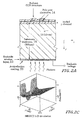
- FIG 2A schematically illustrates the inventive combination as used in a backside-illuminated charge-coupled device (CCD).
- CCD charge-coupled device
- Photons enter the device from the photon-transparent electrically-conducting backside layer 12.
- This layer also acts as an electrical contact so that a bias voltage may be placed between it and the gate circuitry 14 on the front side.
- the n-- type silicon substrate 16 is typically a wafer as supplied by the wafer manufacturer, having a thickness 18 between about 250 ⁇ m and about 1000 ⁇ m (or about 1 mm).
- the substrate can be as thick as 4 or 5 mm.
- an anitreflecting layer 20 is deposited on top of the backside window (not shown to scale). It's thickness and composition is determined by well known rules for antireflective coatings.
- ITO indium tin oxide
- Figure 2B shows a two-dimensional simulation of one pixel of a CCD on high-resistivity silicon substrate, as shown in Fig. 2A. Equipotential lines are shown at a spacing of 0.5V. The collecting gate is biased a -5V and the barrier phases are at 5 V.
- Figure 2C shows the simulated two dimensional potential distribution for a three-phase 15 ⁇ m pixel. This figure shows essentially the same data as Figure 2B but in three dimensions instead of two.
- a channel implant of 1.5 ⁇ 10 12 cm -2 was used.
- the backside bias voltage generated a drift field that extended to the backside electrical contact (the y dimension in fig. 2C).
- bias voltage to the backside layer is key for the operation of the inventive photon detecting element.
- the backside voltage fully charge depletes the photosensitive volume, limits charge spreading, and improves on-chip transistor characteristics. (see Fig. 2 of the IEDM paper cited below).
- the voltage must be well below the breakdown voltage corresponding to an electric field, which ;for silicon is about 2 X 10 5 V/cm at room temperature ( S.M. Sze, Physics of Semiconductor Devices, 2nd Ed. , John Wiley and Sons, p. 103, 1981 ).
- High resistivity substrate, having an extremely low number of charge carriers (N) is specially manufactured so that full charge depletion can be achieved at a low backside voltage.
- the substrate can be fully depleted of charge carriers by applying a sufficient voltage, the substrate thickness can be significantly thicker than in conventional back-illuminated CCDs.
- the thicker substrate has several advantages, including mechanical strength, absorption of long wavelength photons, and economy of manufacture.
- the substrate thickness ( 8 in Figure 1 and 1 8 in Figure 2A) in the inventive combination is between about 100 ⁇ m and about 5 mm.
- the lower thickness limit of the substrate it is more preferable for the lower thickness limit of the substrate to be about 200 ⁇ .
- the lower limit of substrate thickness it is even more preferable for the lower limit of substrate thickness to be about 250 ⁇ .
- a substrate thickness of 10 mm is used to detect energetic x-ray photons because of their long absorption length.
- a substrate thickness is used that is between about 2 and about 3 times the absorption length of the photon of interest. So, for example, to detect a photon in the near infrared (IR) a substrate thickness of about 300 ⁇ m works well.
- the thickness of the inventive electrically-conducting photon-transparent backside layer is partly a function of the type of radiation that will be sensed by the detector. For short wavelength photons the back layer should be very thin. For long wavelength photons the backside layer may be thicker. The functional limit to the thickness of the backside layer is that it must be transparent to the incoming photon that is targeted for detection. As the backside layer is made progressively thicker, it becomes opaque to short wavelength photons.
- the conducting backside layer has been made successfully having a thickness between about 10 nm and about 100 ⁇ m depending on the utility of the detector.
- a backside layer thickness of 100 ⁇ m is just under the silicon band gap and would only be transparent to photons having a wavelength between about 1000 nm and 1100 nm.
- a backside layer thickness of 10 ⁇ m is transparent to photons having a wavelength between about 800 nm and 1100 nm.
- 10 ⁇ m layer of polysilicon would take about 60 hours to deposit. More commonly inventive photon detectors are made with a backlayer that is between about 10 nm and about 1 ⁇ m.
- a backside layer thickness of 1 ⁇ m is transparent to photons having a wavelength between about 550 nm and 1100 nm, which includes red and infra-red.
- a backside layer that is between 10 nm and 100 nm is transparent to blue photons as well as longer wavelength photons and several devices having backside layers in this thickness range have been made.
- the most useful range of backside layer thicknesses is between about 10 nm and about 50 nm because that is transparent to both short and long wavelength photons and the time required for the deposition step is shorter than for the thicker backside layers.
- the photon absorption length in silicon is temperature dependent, with absorption length increasing with decreasing temperature. If a substrate thickness is more than 2 or 3 times the absorption length of the detected photon, excessive backside voltage may be required for charge depletion. The backside voltage required to for full charge depletion increases as the square of the substrate thickness. In addition, there is some loss in resolution when the substrate thickness is larger than necessary to absorb the photon.
- the polysilicon layer is in-situ doped to be electrically conducting. Doping is the addition of elements to the polysilicon that increase the electrical conductivity.
- the window layer is optically thin to be transparent to short-wavelength light which has a small absorption depth in silicon.
- the inventive combination has particularly good long-wavelength response because the silicon wafer does not need to be thinned. Because the active volume (the thickness of the silicon wafer) is much thicker than typical CCDs or other sensors, long-wavelength photons such as those in the infrared region are absorbed in the active volume of the silicon and generate charge carriers instead of passing through.
- the thin backside polysilicon layer acts as a transparent electrical contact that allows for application of a bias voltage to deplete the substrate. Because of the large refractive index of silicon (3.7), the layer has fairly high reflectivity. For example, reflectivity is 33% at long wavelengths and even more at short wavelengths. Application of a conducting coating that reduces reflectivity of the backside window layer increases the quantum efficiency of the inventive combination.
- the inventive combination of transparent low-resistivity backside layer and silicon wafer is additionally combined with an antireflecting layer ( 10 in fig. 1 or 20 in fig. 2).
- the antireflecting layer is electrically conducting and transparent, for example, indium tin oxide (ITO). Coating the in-situ doped polysilicon with ITO leads to less reflection loss and thus better quantum efficiency. Using a conducting outer layer additionally decreases series resistance thus making a lower noise device. A reduction in dark current of about a factor of two was observed when an ITO coating was applied to the combined backside layer and silicon wafer.
- the ITO layer was deposited by reactive sputtering. Ionized argon atoms are attracted to a biased ITO target and sublimate off ITO molecules. The molecules are deposited on the backside layer of the substrate by locating it directly across from the ITO target.
- a major advantage of the inventive combination is that the backside window layer is transparent to full spectrum of photons, from uv through IR and including x-rays, which can enter the active silicon volume 6 and create charge carriers. Applying the backside window to a relatively thick silicon wafer has several advantages.
- the thickness of the active silicon volume can be chosen to absorb, and thus detect, long-wavelength photons, that same thickness can lead to loss of charge carriers created by short-wavelength photons, for example in the blue or uv region.
- a voltage is applied between the conducting backside window layer (or optional ITO coating) and the p+ region of a photodiode.
- the voltage is applied between the conducting backside window layer (optionally having an ITO and or other antireflective coating(s)) and a polysilicon gate.
- the gate electrodes result in a voltage drop across the buried channels, and the difference between the voltage at the buried channel junction and the backside voltage determines the electric field that the carriers drift through ( S. Holland et al. "Development of back-illuminated, fully-depleted CCD image sensors for use in astronomy and astrophysics", IEEE Workshop on Charge-Coupled Devices & Advanced Image Sensors, Bruge, Belgium, June 5-7, 1997 ).
- the polysilicon layer can withstand bias voltages necessary to fully deplete a high-resistivity substrate without causing significant increases in dark current.
- the bias voltage causes the small number of mobile electrons in the high-resistivity n-type substrate to be removed, leaving behind ionized donor atoms which result in the electric field necessary to collect the photogenerated charges before they recombine or diffuse out, which would cause a loss of spatial resolution.
- CCD columns are isolated from another with a channel stop implant, which is an ion implant resulting in a larger concentration of dopant impurities at the surface of the CCD than in the bulk. The effect is to raise the potential barrier between adjacent columns.
- a bias voltage between the backside window and the frontside of a photon detection device creates a fully charge depleted photon sensitive volume. It also improves spatial_resolution by limiting the charge spread, or bloom, as the photon created charge carriers move toward the front side of the detector.
- the bias voltage V B is chosen based on several factors, including the resistance of the photon-sensitive silicon volume.
- V D ( 0.5 q N x D 2 ) / ⁇ s
- N is the number of dopant atoms per cm 3 in the depleted region
- x D is the length of the depleted region
- q is the electronic charge (1.602 10 -19 C)
- ⁇ s is the permittivity of silicon (1.0 10 -12 F/cm).
- Table I compares ⁇ and N for various high-resistivity CCDs (assuming about 500 cm 2 /V-sec for hole mobility, and 1500 cm 2 /V-sec for electron mobility): Table I researchers Substrate doping ⁇ N epi ? Reported x D Lincoln1 p 6.5K 1.9 ⁇ 10 12 no 50 ⁇ m Lincoln2 p 1.0K 1.3 ⁇ 10 13 no ? Lincoln3 p 5-10K 1.3 ⁇ 10 12 no >50 ⁇ m NorthernTele p 1-5K 2.5 ⁇ 10 12 no >50 ⁇ m Sheffield p 8K 1.5 ⁇ 10 12 no 80 ⁇ m Dalsa p 1K 1.3 ⁇ 10 13 yes 40 ⁇ m MPI n 2.5K 1.7x10 12 yes 300 ⁇ m Westinghouse n 15K 2. 8x10 11 no 250 ⁇ m Present Invention n >10K ⁇ 4.1x10 11 no 300 ⁇ m
- Extremely low N is needed to deplete a substrate of between 100 ⁇ m and 1000 ⁇ m with reasonable voltages.
- the present invention has been fabricated having sufficiently low N.
- the other substrate developed by Westinghouse researchers, having low N, exhibited excessively high dark currents, much higher than could be used in a useful device.
- the lower the N the better the performance of the inventive device ( D.M. McCann et al., "Area array x-ray sensors," Advances in Focal Plane Technology, Proc. of SPIE, 217, pp. 118-128, 198 ).
- the advantage to using low N is that the substrate can be depleted with relatively low voltages (about 20-25V). This makes the breakdown problem less likely and decreases concern over problems with either or both of the CCD pixels or output amplifier. Both concerns are due to the strongly two-dimensional nature of the fields for extremely low N. Transistor and CCD properties improve with increasing backside voltage, provided the voltage remains less than breakdown voltage. The strong two-dimensional nature of the fields and the backside voltage tend to somewhat flatten the two-dimensional fields. The effect of backside voltage on CCD output transistor characteristics is discussed in S. Holland et al., "A 200 X 200 CCD Image Sensor fabricated on high-resistivity silicon", International Electron Devices Meeting (IEDM) Technical Digest, pp 911-14, 1996, San Francisco CA .
- the reflection loss can be decreased by using antireflection coatings.
- Silicon dioxide an insulator with refractive index 1.405
- indium tin oxide a conductor which is also transparent and has a refractive index of 1.8-2.2
- ITO thickness was tuned to the desired wavelength where the scintillating crystals emitted photons of a particular wavelength ( S. Holland et al., Development of low noise, backside illuminated silicon photodiode arrays", IEEE Transaction on Nuclear Science, 44(3); 443-7, June 1997 ). About a quarter wavelength thickness of ITO was deposited.
- Another approach is to use two coating for antireflective properties, an underlayer of ITO and a top layer of silicon dioxide. Techniques of antireflective coatings are well developed and can be applied to the backside window of the inventive combination. Two sources of such materials and discussion is a paper by M. Blouke and M.D.
- TCOs transparent conducting oxides
- any film that has a low refractive index can be used as an antireflection coating, although a highly resistive layer could result in an undesirably nonuniform backside voltage under some circumstances, for example with a very bright image.
- Other candidate materials for antireflection coatings include, hafnium oxide, lead oxide, and aluminum oxide, silicon nitride, and magnesium fluoride.
- An insulating layer such as MgF is compatible with the thin polysilicon backside layer are multi-layer coatings. However if a insulating material is used as an antireflective layer, part of the insulator would have to be removed in order to make backside contact, or the voltage can be applied to the frontside and the backside allowed to float.
- a CCD fabricated using high resistivity silicon substrate as the photon sensitive volume is one aspect of the present invention. It is surprising that a CCD fabricated with such high resistivity silicon works usefully, with or without the electrically conducting layer on the backside.
- the high-resistivity volume makes the potentials strongly two-dimensional and many people expected that potential wells wouldn't form functionally in such high-resistivity material. Pixels were made as small as 15x15 ⁇ m 2 on the inventive device. It was unexpected that we would be able to make such small pixels on high-resistivity material.
- Commercial devices on lower resistivity silicon had pixel sizes of either 27X27 ⁇ m 2 or 18X24 ⁇ m 2 .
- the backside layer is doped to between about 0.0001 to about 10 atomic percent doping with phosphorous. More preferably it is doped to between about 0.001 to about 3 atomic percent with phosphorous. Most preferably it is doped to between about .1 to about 3 atomic percent with phosphorous.
- Working models have been constructed using about 1 and about 1.5 atomic percent phosphorous doping, without annealing. This is described in more detail in the IEEE Transaction on Nuclear Science paper cited above.
- the dark current in the CCD has both a bulk component and a surface component.
- the effective gettering from the phosphorus-doped polysilicon layer greatly reduces the bulk component, leaving the surface component as the dominant source of dark current.
- Techniques for reducing the surface current involve filling the interface states at the surface with carriers supplied from the channel stop implant.
- the polysilicon gate electrode on the front of the device is biased so that an inversion layer of carriers is created, filling the surface states. Once filled the states no longer contribute to the dark current.
- the high concentration of mobile carriers at the surface pins the potential, hence the term surface pinning.
- This technique requires that the channel stop implant be biased (typically at ground potential).
- Oxides on silicon always have a fixed positive charge at the interface.
- this positive charge forms a small depletion layer at the back surface.
- For short wavelength photons the generated electrons are attracted by the fixed charge towards the back surface.
- a solution is UV charging of the back surface to create a surface layer of electrons to overcome the fixed positive charge.
- Another technique is the flash gate where the workfunction of the thin transparent gate overcomes the positive charge.
- RCA researchers made a conventional low resistivity CCD on n-type silicon where the positive charge works repelled the holes towards the potential wells.
- the present invention when a backside voltage is applied the problem disappears. Even if a CCD was made on p-type substrate, using the present invention a backside voltage large enough to deplete the substrate of charges would more than compensate for the positive charge.
- the inventive backside window is deposited by low pressure chemical vapor deposition (CVD) of silane (SiH 4 ) in the presence of phosphine (PH 3 ) on to a high resistivity silicon substrate.
- the process is performed at low temperatures, about 650°C, and is performed under extremely clean conditions; impurities are kept to less than parts per billion. Because it is a low temperature step, deposition of the polycrystalline silicon (polysilicon) layer is done near the end of the processing, after all the high temperature processing is complete.
- the process protocols below illustrate one sequence for applying the window.
- the vacuum chamber sidewalls are covered with polysilicon that deposits on the chamber walls. Gasses used are pure to 99.999%.
- the silicon wafers are precleaned by exacting, if generally accepted, protocol.
- the substrate is put through a gettering process before the backside window is deposited.
- a thick, phosphorus doped polysilicon is used for gettering, and then is etched off before the backside window is deposited.
- the gettering step is performed according to a method published by S. Holland in Nuclear Instruments and Methods in Physics Research, A275,537-541, 1989, entitled, "Fabrication of detectors and transistors on high-resistivity silicon ". This process gives a substrate that is essentially free of metallic contaminants.
- the backside layer is doped to between about 0.0001 to about 10 atomic percent doping with phosphorous. More preferably it is doped to between about 0.001 to about 3 atomic percent with phosphorous. Most preferably it is doped to between about .1 to about 3 atomic percent with phosphorous.
- Working models have been constructed using about 1 atomic percent phosphorous doping, without annealing.
- deposition of the thin backside polysilicon window is performed by the following steps:
- the process is performed at about 650°C, 400 milliTorr pressure, using a gas flow of 1% PH 3 in SiH 4 .
- Example 2 obtaining Low N substrate
- Example 3 Making a photodiode having an electrically conducting, photon transparent, backside layer.
- Starting material silicon wafer for substrate having: resistance greater than 4k ⁇ -cm, 300 ⁇ m thick, ⁇ 100> n-type silicon (custom ordered from Wacker).
- Starting material silicon wafer for substrate having: resistance greater than 4k ⁇ -cm, 300 ⁇ m thick, ⁇ 100> n-type silicon (custom ordered from Wacker).
- the ITO layers were deposited at room temperature by RF magnetron sputtering from a target composed of 90 wt.% In 2 O 3 and 1- wt% SnO 2 (target area 12 cm by 38 cm).
- the power used for all deposition was 500 W.
- the conduction in ITO is due to oxygen vacancies, and therefore the oxygen concentration in the film must be well controlled.
- the films were reactively sputtered in a mixtures of O 2 and Ar.
- the total sputter pressure was varied from 2-8 mTorr and the O 2 concentration was varied from 0-5% in order to determine deposition conditions that would yield films with low resistivity and high optical transmittance.
- R ⁇ In(1/ t ) the thickness-independent quantity, R ⁇ In(1/ t ), was used as a figure of merit, where R ⁇ is the sheet resistance and t is the optical transmittance at a given wavelength.
- the sheet resistance of the films was measured using a four-point probe, and the optical transmittance was measured using a dual-beam spectrophotometer with a tungsten halogen lamp. Plotted as a function of O 2 partial pressure during film deposition, R ⁇ 1n (1/ t ) exhibits a noticeable minimum; the best films result at O 2 partial pressures of 0.04-0.08 mTorr.
- ITO In the back contact to the photodiode arrays, ITO was deposited at a total pressure of 2 mTorr and an O 2 partial pressure of 0.06 mTorr. At these depositions conditions, the films exhibited resistivities of ⁇ 4.8X10 -4 ⁇ -cm. A low temperature, post-deposition anneal further improved the quality of the films: a one hour anneal at 200 °C in N 2 lowered the resistivity to ⁇ 3.4 ⁇ 10 -4 ⁇ -cm.
- Example 6 Image of a test pattern using 400 nm light.
- CCDs were fabricated with a 20 nm backside polysilicon layer.
- an antireflection coating of approximately 50 nm of ITO was sputter deposited over the polysilicon ( S. Holland et al., "Development of low noise, backside illuminated silicon photodiode arrays", IEEE Transaction on Nuclear Science, 44(3); 443-7, June 1997 ).
- This layer was electrically conducting and reduced the resistance of the backside contact in addition to acting as an antireflection coating.
- CCDs were mounted on specially designed aluminum nitride circuit board having an opening for backside illumination'.
- Aluminum nitride was chosen for its excellent coefficient of thermal expansion match to silicon, in addition to its high thermal conductivity.
- a standard package used at Lick Observatory was modified to accommodate the aluminum nitride substrates.
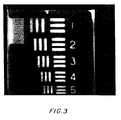
- Figure 3 shows a test pattern image taken with a back-illuminated CCD at - 120°C. The backside voltage was 25 V and resulted in over-depletion of the substrate.
- the wavelength of the incident light was 400 nm.
- the absorption depth in silicon at this wavelength is approximately 0.2 ⁇ m.
- the photon-generated charge carriers must therefore drift to the CCD potential wells located 300 ⁇ m away.
- Figure 3 demonstrates use of the inventive CCD to image short wavelength photons from the backside of a 300 ⁇ m thick silicon substrate. Preliminary measurements show that the quantum efficiency for 400 nm photons is approximately 67%. In addition, first measurements indicate that lateral charge diffusion at 25V backside voltage was about one pixel width.
- Example 7 Quantum efficiency as a function of wavelength for a p-i-n photodiode having a various thicknesses of backside layers, and no antireflective coating.
- Figure 4 shows the measured quantum efficiency versus wavelength for back-illuminated photodiodes with varying backside-polysilicon-layer thicknesses.
- the short wavelength response improves with .decreasing polysilicon thickness.
- the response in the near infrared extends to a wavelength of approximately 1 ⁇ m.
- the quantum efficiency was measured by comparison to a photodiode with a known spectral response.
- the light passed through a monochromator and was focused on the test photodiode and the calibrated photodiode via optical fibers.
- Example 8 Quantum efficiency as a function of wavelength for a p-i-n photodiode having a various thicknesses of backside layers, and having an antireflective coating.
- X ITO is the ITO film thickness that minimizes reflection at the wavelength X
- n is the refractive index of ITO.
- Figure 5 shows the quantum efficiency as a function of wavelength for a back-illuminated, 300 ⁇ m thick p-i-n photodiode having a 10 nm backside layer coated with 57 nm ITO (solid line).
- the inventive photodiode was operated at room temperature (Ibid. IEEE Nuc. Sci.).
- the thickness was chosen to maximize the quantum efficiency at the 415 nm wavelength of a photon emitted from lutetium orthosilicate (LSO).
- LSO lutetium orthosilicate
- the improvement in quantum efficiency due to the antireflective coating exceeds 60% over a 100 nm wavelength range and peaks at ⁇ - 450 nm, close to the target value.
- the combination a thin polysilicon contact and quarter-wave ITO layer yields a QE of approximately 75% at the LSO wavelength.
- BGO bismuth germanate
- the quantum efficiency was even higher, about 90 % at 480 nm. It could be further improved by optimizing the ITO thickness for the BGO wavelength.
- the circular data points were taken from a CCD made with the inventive combination of a 300 ⁇ m silicon substrate having a 10 nm conducting backside layer of polysilicon, coated with approximately 57 nm ITO.
- the CCD was used in an astronomical camera operated at -120°C.
- the broken line shows data taken with a conventional back-illuminated CCD, fabricated on a thinned, low resistance silicon substrate and having a standard antireflective coating ( M. Blouke and M.D. Nelson, “Stable ultraviolet antireflection coatings for charge-coupled devices", SPIE 1900; 228-240, 1993 ).
- Example 9 Charge diffusion as a function of backside voltage.
- the mask was laid directly on the back surface of the CCD and illuminated using 400 nm light from a small light source. The backside voltage was then varied and images were obtained. The root-mean-square (RMS) spreads in x and y for each spot were computed and the average is plotted as a function of voltage in figure 6.
- RMS root-mean-square
- the backside voltage of a 300 ⁇ m thick CCD is 25 volts (described in detail in S. Holland et al. "Development of back-illuminated, fully-depleted CCD image sensors for use in astronomy and astrophysics", IEEE Workshop on Charge-Coupled Devices & Advanced Image Sensors, Bruge, Belgium, June 5-7, 1997 ).
- the invention provides an electrically conducting layer attached to the backside of a high resistivity silicon detector and bias voltage applied between the backside and front patterned side of the detector.
- the electrically conducting layer can be thin enough to be transparent to short wavelength photons (such as blue) or long wavelength photons or both, as needed for the particular application.
- Some devices for which the invention has been found useful are photodiodes, CCDs (particularly for low light-circumstances), x-ray Detector; and direct detection of x-rays (using an active volume thickness of 300 ⁇ m, sensitivity to about 5.9 keV x-rays was achieved). In principle, using thicker substrates enables higher energy x-rays to be detected.
- the backside window layer can withstand bias voltages necessary to fully deplete the high-resistivity substrate without causing significant increases in dark current (the bias voltage causes the small number of mobile electrons in the high-resistivity n-type substrate to be removed, leaving behind ionized donor atoms which result in the electric field necessary to collect the photogenerated charges before they recombine or diffuse out, which would cause a loss of spatial resolution).
Landscapes
- Solid State Image Pick-Up Elements (AREA)
- Light Receiving Elements (AREA)
Applications Claiming Priority (2)
| Application Number | Priority Date | Filing Date | Title |
|---|---|---|---|
| US3041596P | 1996-11-01 | 1996-11-01 | |
| EP97950582A EP0950264A4 (de) | 1996-11-01 | 1997-10-31 | Mit photoempfindlichem siliziumdetektor verbundenes phototransparentes fenster mit niedrigem widerstand |
Related Parent Applications (1)
| Application Number | Title | Priority Date | Filing Date |
|---|---|---|---|
| EP97950582A Division EP0950264A4 (de) | 1996-11-01 | 1997-10-31 | Mit photoempfindlichem siliziumdetektor verbundenes phototransparentes fenster mit niedrigem widerstand |
Publications (2)
| Publication Number | Publication Date |
|---|---|
| EP1855321A2 true EP1855321A2 (de) | 2007-11-14 |
| EP1855321A3 EP1855321A3 (de) | 2008-08-06 |
Family
ID=21854097
Family Applications (2)
| Application Number | Title | Priority Date | Filing Date |
|---|---|---|---|
| EP07016419A Withdrawn EP1855321A3 (de) | 1996-11-01 | 1997-10-31 | Rückbeleuchteter und vollständig verarmter CCD mit einer transparenten Fensterschicht mit geringem eletrischem Widerstand |
| EP97950582A Withdrawn EP0950264A4 (de) | 1996-11-01 | 1997-10-31 | Mit photoempfindlichem siliziumdetektor verbundenes phototransparentes fenster mit niedrigem widerstand |
Family Applications After (1)
| Application Number | Title | Priority Date | Filing Date |
|---|---|---|---|
| EP97950582A Withdrawn EP0950264A4 (de) | 1996-11-01 | 1997-10-31 | Mit photoempfindlichem siliziumdetektor verbundenes phototransparentes fenster mit niedrigem widerstand |
Country Status (5)
| Country | Link |
|---|---|
| US (1) | US6025585A (de) |
| EP (2) | EP1855321A3 (de) |
| JP (2) | JP4446292B2 (de) |
| AU (1) | AU5354698A (de) |
| WO (1) | WO1998020561A1 (de) |
Cited By (1)
| Publication number | Priority date | Publication date | Assignee | Title |
|---|---|---|---|---|
| US11295962B2 (en) | 2018-07-10 | 2022-04-05 | The Board Of Trustees Of The Leland Stanford Junior University | Low temperature process for diode termination of fully depleted high resistivity silicon radiation detectors that can be used for shallow entrance windows and thinned sensors |
Families Citing this family (44)
| Publication number | Priority date | Publication date | Assignee | Title |
|---|---|---|---|---|
| US6259085B1 (en) * | 1996-11-01 | 2001-07-10 | The Regents Of The University Of California | Fully depleted back illuminated CCD |
| WO1998020561A1 (en) * | 1996-11-01 | 1998-05-14 | Lawrence Berkeley Laboratory | Low-resistivity photon-transparent window attached to photo-sensitive silicon detector |
| EP0999698B1 (de) * | 1998-11-02 | 2013-06-19 | Canon Kabushiki Kaisha | Festkörper-Bildaufnahmevorrichtung und entsprechendes Resetverfahren |
| US6534773B1 (en) * | 1998-11-09 | 2003-03-18 | Photon Imaging, Inc. | Radiation imaging detector and method of fabrication |
| JP2003504856A (ja) * | 1999-07-02 | 2003-02-04 | ディジラッド・コーポレーション | 半導体装置に対する間接的裏面コンタクト |
| US20010054723A1 (en) * | 2000-03-17 | 2001-12-27 | Tadashi Narui | Image sensor, method of fabricating the same, and exposure apparatus, measuring device, alignment device, and aberration measuring device using the image sensor |
| US20020020846A1 (en) * | 2000-04-20 | 2002-02-21 | Bo Pi | Backside illuminated photodiode array |
| WO2001082382A1 (en) | 2000-04-20 | 2001-11-01 | Digirad Corporation | Fabrication of low leakage-current backside illuminated photodiodes |
| US6426991B1 (en) | 2000-11-16 | 2002-07-30 | Koninklijke Philips Electronics N.V. | Back-illuminated photodiodes for computed tomography detectors |
| US6466645B1 (en) | 2000-11-22 | 2002-10-15 | Ge Medical Systems Global Technology Company, Llc | Methods and apparatus for tube-spit correction |
| US6498073B2 (en) | 2001-01-02 | 2002-12-24 | Honeywell International Inc. | Back illuminated imager with enhanced UV to near IR sensitivity |
| US6713768B2 (en) | 2001-04-16 | 2004-03-30 | Photon Imaging, Inc. | Junction-side illuminated silicon detector arrays |
| US6510195B1 (en) * | 2001-07-18 | 2003-01-21 | Koninklijke Philips Electronics, N.V. | Solid state x-radiation detector modules and mosaics thereof, and an imaging method and apparatus employing the same |
| JP2003166047A (ja) * | 2001-09-20 | 2003-06-13 | Shin Meiwa Ind Co Ltd | ハロゲン化合物の成膜方法及び成膜装置、並びにフッ化マグネシウム膜 |
| JP4123415B2 (ja) * | 2002-05-20 | 2008-07-23 | ソニー株式会社 | 固体撮像装置 |
| EP1532691B1 (de) * | 2002-08-29 | 2009-02-11 | X-FAB Semiconductor Foundries AG | Minimierung von lichtverlusten und elektronische abschirmung an integrierten fotodioden |
| US7126100B1 (en) * | 2004-05-21 | 2006-10-24 | Kla-Tencor Technologies Corporation | System and method for sensing using adjustable modulation transfer function (MTF) |
| JP4211696B2 (ja) * | 2004-06-30 | 2009-01-21 | ソニー株式会社 | 固体撮像装置の製造方法 |
| US7816653B2 (en) * | 2004-08-20 | 2010-10-19 | Artto Aurola | Semiconductor radiation detector with a modified internal gate structure |
| DE102004055677A1 (de) * | 2004-11-18 | 2006-06-01 | Fraunhofer-Gesellschaft zur Förderung der angewandten Forschung e.V. | Chipträgerverbund und Verfahren zum Herstellen eines Chipträgerverbunds |
| US7271468B2 (en) * | 2005-02-16 | 2007-09-18 | The Regents Of The University Of California | High-voltage compatible, full-depleted CCD |
| US7605397B2 (en) * | 2005-08-17 | 2009-10-20 | Digirad Corporation | Capacitive bypass |
| JP4680763B2 (ja) * | 2005-12-16 | 2011-05-11 | 住友電工デバイス・イノベーション株式会社 | 電子装置および半導体装置 |
| WO2007077286A1 (en) * | 2006-01-05 | 2007-07-12 | Artto Aurola | Semiconductor radiation detector detecting visible light |
| US8491997B2 (en) | 2006-06-22 | 2013-07-23 | Sabic Innovative Plastics Ip B.V. | Conductive wire comprising a polysiloxane/polyimide copolymer blend |
| DE602007002018D1 (de) * | 2006-06-28 | 2009-10-01 | St Microelectronics Sa | Von hinten beleuchtete Bildaufnahmevorrichtung |
| US7800040B2 (en) * | 2006-09-21 | 2010-09-21 | California Institute Of Technology | Method for growing a back surface contact on an imaging detector used in conjunction with back illumination |
| WO2009146264A1 (en) * | 2008-05-30 | 2009-12-03 | Sarnoff Corporation | Method for electronically pinning a back surface of a back-illuminated imager fabricated on a utsoi wafer |
| GB2466502B (en) * | 2008-12-23 | 2013-09-04 | E2V Tech Uk Ltd | CCD Sensor |
| GB2475086B (en) | 2009-11-05 | 2014-02-05 | Cmosis Nv | Backside illuminated image sensor |
| EP2526566B1 (de) * | 2010-01-21 | 2018-03-07 | Roper Scientific, Inc. | Rückbeleuchteter festkörper-photonensensor und herstellungsverfahren dafür |
| JP5351066B2 (ja) * | 2010-01-25 | 2013-11-27 | 浜松ホトニクス株式会社 | Oct装置 |
| US8692198B2 (en) * | 2010-04-21 | 2014-04-08 | Sionyx, Inc. | Photosensitive imaging devices and associated methods |
| JP5818238B2 (ja) * | 2010-10-06 | 2015-11-18 | ラピスセミコンダクタ株式会社 | 半導体装置 |
| US9165971B2 (en) | 2010-10-25 | 2015-10-20 | California Institute Of Technology | Atomically precise surface engineering for producing imagers |
| JP5766062B2 (ja) * | 2011-08-05 | 2015-08-19 | キヤノン株式会社 | 軟x線検出装置、及び軟x線検出システム |
| WO2014205706A1 (zh) * | 2013-06-26 | 2014-12-31 | 林大伟 | 光电二极管 |
| US20150084152A1 (en) * | 2013-09-24 | 2015-03-26 | Da Wei Lin | Photodiode |
| JP6595750B2 (ja) * | 2014-03-14 | 2019-10-23 | キヤノン株式会社 | 固体撮像装置及び撮像システム |
| US9553116B2 (en) | 2014-06-05 | 2017-01-24 | Teledyne Scientific & Imaging, Llc | Imaging detector having an integrated wide bandgap layer and method of manufacturing thereof |
| CN106325572A (zh) * | 2015-06-24 | 2017-01-11 | 宸鸿科技(厦门)有限公司 | 用于形变感测的透明导电氧化物薄膜 |
| US10396219B2 (en) * | 2016-06-16 | 2019-08-27 | Arizona Board Of Regents On Behalf Of Arizona State University | Transparent conductive oxide in silicon heterojunction solar cells |
| JP6451881B1 (ja) * | 2018-01-24 | 2019-01-16 | 株式会社Sumco | シリコン層の評価方法およびシリコンエピタキシャルウェーハの製造方法 |
| WO2021205662A1 (ja) * | 2020-04-10 | 2021-10-14 | 株式会社オプトハブ | 半導体イメージセンサ |
Family Cites Families (11)
| Publication number | Priority date | Publication date | Assignee | Title |
|---|---|---|---|---|
| BE793094A (fr) * | 1971-12-23 | 1973-04-16 | Western Electric Co | Dispositif de formation d'images a transfert de charge |
| NL7407811A (nl) * | 1974-06-12 | 1975-12-16 | Philips Nv | Fotodiode. |
| JPS57124482A (en) * | 1981-01-27 | 1982-08-03 | Nippon Telegr & Teleph Corp <Ntt> | Solar cell |
| US4570329A (en) * | 1984-08-15 | 1986-02-18 | Honeywell Inc. | Apparatus and method for fabricating backside mosaic of photoconductive infrared detectors |
| US4695861A (en) * | 1985-10-21 | 1987-09-22 | Honeywell Inc. | Backside mosaic photoconductive infrared detector array |
| US5005063A (en) * | 1986-03-03 | 1991-04-02 | California Institute Of Technology | CCD imaging sensor with flashed backside metal film |
| JPH0763090B2 (ja) * | 1986-03-19 | 1995-07-05 | ソニー株式会社 | 固体撮像装置 |
| US4774557A (en) * | 1986-05-15 | 1988-09-27 | General Electric Company | Back-illuminated semiconductor imager with charge transfer devices in front surface well structure |
| US5189297A (en) * | 1988-08-29 | 1993-02-23 | Santa Barbara Research Center | Planar double-layer heterojunction HgCdTe photodiodes and methods for fabricating same |
| US5494833A (en) * | 1994-07-14 | 1996-02-27 | The United States Of America As Represented By The Secretary Of The Air Force | Backside illuminated MSM device method |
| WO1998020561A1 (en) * | 1996-11-01 | 1998-05-14 | Lawrence Berkeley Laboratory | Low-resistivity photon-transparent window attached to photo-sensitive silicon detector |
-
1997
- 1997-10-31 WO PCT/US1997/020173 patent/WO1998020561A1/en not_active Ceased
- 1997-10-31 JP JP52175398A patent/JP4446292B2/ja not_active Expired - Lifetime
- 1997-10-31 AU AU53546/98A patent/AU5354698A/en not_active Abandoned
- 1997-10-31 US US08/961,868 patent/US6025585A/en not_active Expired - Lifetime
- 1997-10-31 EP EP07016419A patent/EP1855321A3/de not_active Withdrawn
- 1997-10-31 EP EP97950582A patent/EP0950264A4/de not_active Withdrawn
-
2006
- 2006-07-31 JP JP2006208626A patent/JP4972360B2/ja not_active Expired - Lifetime
Cited By (1)
| Publication number | Priority date | Publication date | Assignee | Title |
|---|---|---|---|---|
| US11295962B2 (en) | 2018-07-10 | 2022-04-05 | The Board Of Trustees Of The Leland Stanford Junior University | Low temperature process for diode termination of fully depleted high resistivity silicon radiation detectors that can be used for shallow entrance windows and thinned sensors |
Also Published As
| Publication number | Publication date |
|---|---|
| JP4446292B2 (ja) | 2010-04-07 |
| JP4972360B2 (ja) | 2012-07-11 |
| AU5354698A (en) | 1998-05-29 |
| EP0950264A4 (de) | 2000-04-26 |
| JP2006324686A (ja) | 2006-11-30 |
| EP0950264A1 (de) | 1999-10-20 |
| US6025585A (en) | 2000-02-15 |
| JP2001503918A (ja) | 2001-03-21 |
| EP1855321A3 (de) | 2008-08-06 |
| WO1998020561A1 (en) | 1998-05-14 |
Similar Documents
| Publication | Publication Date | Title |
|---|---|---|
| US6025585A (en) | Low-resistivity photon-transparent window attached to photo-sensitive silicon detector | |
| WO1998020561A9 (en) | Low-resistivity photon-transparent window attached to photo-sensitive silicon detector | |
| US7297927B2 (en) | Fabrication of low leakage-current backside illuminated photodiodes | |
| US7422924B2 (en) | Image device and photodiode structure | |
| US7217589B2 (en) | Deep photodiode isolation process | |
| US5719414A (en) | Photoelectric conversion semiconductor device with insulation film | |
| US20140252524A1 (en) | Array of mutually isolated, geiger-mode, avalanche photodiodes and manufacturing method thereof | |
| US20090026511A1 (en) | Isolation process and structure for CMOS imagers | |
| EP1045450A2 (de) | Bildsensoranordnung | |
| US12266671B2 (en) | Photodetectors with a deep trench isolation region that includes a bragg mirror | |
| Holland et al. | A 200/spl times/200 ccd image sensor fabricated on high-resistivity silicon | |
| Brown et al. | Transparent metal oxide electrode CID imager | |
| US20070045682A1 (en) | Imager with gradient doped EPI layer | |
| KR100709645B1 (ko) | 방사 경화된 가시성 p-i-n 검출기 | |
| JPH0730081A (ja) | 高エネルギ粒子検出用電荷結合型半導体装置及びその製造方法 |
Legal Events
| Date | Code | Title | Description |
|---|---|---|---|
| PUAI | Public reference made under article 153(3) epc to a published international application that has entered the european phase |
Free format text: ORIGINAL CODE: 0009012 |
|
| AC | Divisional application: reference to earlier application |
Ref document number: 0950264 Country of ref document: EP Kind code of ref document: P |
|
| AK | Designated contracting states |
Kind code of ref document: A2 Designated state(s): AT BE CH DE DK ES FI FR GB GR IE IT LI LU MC NL PT SE |
|
| AX | Request for extension of the european patent |
Extension state: AL LT LV RO SI |
|
| RIC1 | Information provided on ipc code assigned before grant |
Ipc: H01L 31/105 20060101ALI20071016BHEP Ipc: H01L 29/768 20060101ALI20071016BHEP Ipc: H01L 27/148 20060101AFI20071016BHEP |
|
| RTI1 | Title (correction) |
Free format text: BACK-ILLUMINATED FULLY DEPLETED CHARGE COUPLED DEVICE COMPRISING LOW-RESISTIVITY TRANSPARENT WINDOW LAYER |
|
| PUAL | Search report despatched |
Free format text: ORIGINAL CODE: 0009013 |
|
| AK | Designated contracting states |
Kind code of ref document: A3 Designated state(s): AT BE CH DE DK ES FI FR GB GR IE IT LI LU MC NL PT SE |
|
| AX | Request for extension of the european patent |
Extension state: AL LT LV RO SI |
|
| RIC1 | Information provided on ipc code assigned before grant |
Ipc: H01L 27/146 20060101ALI20080702BHEP Ipc: H01L 31/105 20060101ALI20080702BHEP Ipc: H01L 27/148 20060101AFI20071016BHEP |
|
| 17P | Request for examination filed |
Effective date: 20090115 |
|
| 17Q | First examination report despatched |
Effective date: 20090223 |
|
| AKX | Designation fees paid |
Designated state(s): AT BE CH DE DK ES FI FR GB GR IE IT LI LU MC NL PT SE |
|
| STAA | Information on the status of an ep patent application or granted ep patent |
Free format text: STATUS: THE APPLICATION IS DEEMED TO BE WITHDRAWN |
|
| 18D | Application deemed to be withdrawn |
Effective date: 20090707 |