EP1855381B1 - Treibereinheit für einen Halbbrückenumrichter - Google Patents
Treibereinheit für einen Halbbrückenumrichter Download PDFInfo
- Publication number
- EP1855381B1 EP1855381B1 EP06009555A EP06009555A EP1855381B1 EP 1855381 B1 EP1855381 B1 EP 1855381B1 EP 06009555 A EP06009555 A EP 06009555A EP 06009555 A EP06009555 A EP 06009555A EP 1855381 B1 EP1855381 B1 EP 1855381B1
- Authority
- EP
- European Patent Office
- Prior art keywords
- switching
- half bridge
- drive unit
- hbc
- time delay
- Prior art date
- Legal status (The legal status is an assumption and is not a legal conclusion. Google has not performed a legal analysis and makes no representation as to the accuracy of the status listed.)
- Expired - Lifetime
Links
Images




Classifications
-
- H—ELECTRICITY
- H02—GENERATION; CONVERSION OR DISTRIBUTION OF ELECTRIC POWER
- H02M—APPARATUS FOR CONVERSION BETWEEN AC AND AC, BETWEEN AC AND DC, OR BETWEEN DC AND DC, AND FOR USE WITH MAINS OR SIMILAR POWER SUPPLY SYSTEMS; CONVERSION OF DC OR AC INPUT POWER INTO SURGE OUTPUT POWER; CONTROL OR REGULATION THEREOF
- H02M1/00—Details of apparatus for conversion
- H02M1/38—Means for preventing simultaneous conduction of switches
-
- H—ELECTRICITY
- H02—GENERATION; CONVERSION OR DISTRIBUTION OF ELECTRIC POWER
- H02M—APPARATUS FOR CONVERSION BETWEEN AC AND AC, BETWEEN AC AND DC, OR BETWEEN DC AND DC, AND FOR USE WITH MAINS OR SIMILAR POWER SUPPLY SYSTEMS; CONVERSION OF DC OR AC INPUT POWER INTO SURGE OUTPUT POWER; CONTROL OR REGULATION THEREOF
- H02M1/00—Details of apparatus for conversion
- H02M1/08—Circuits specially adapted for the generation of control voltages for semiconductor devices incorporated in static converters
-
- H—ELECTRICITY
- H03—ELECTRONIC CIRCUITRY
- H03K—PULSE TECHNIQUE
- H03K17/00—Electronic switching or gating, i.e. not by contact-making and –breaking
- H03K17/28—Modifications for introducing a time delay before switching
- H03K17/284—Modifications for introducing a time delay before switching in field effect transistor switches
-
- H—ELECTRICITY
- H03—ELECTRONIC CIRCUITRY
- H03K—PULSE TECHNIQUE
- H03K17/00—Electronic switching or gating, i.e. not by contact-making and –breaking
- H03K17/51—Electronic switching or gating, i.e. not by contact-making and –breaking characterised by the components used
- H03K17/56—Electronic switching or gating, i.e. not by contact-making and –breaking characterised by the components used by the use, as active elements, of semiconductor devices
- H03K17/687—Electronic switching or gating, i.e. not by contact-making and –breaking characterised by the components used by the use, as active elements, of semiconductor devices the devices being field-effect transistors
- H03K17/6871—Electronic switching or gating, i.e. not by contact-making and –breaking characterised by the components used by the use, as active elements, of semiconductor devices the devices being field-effect transistors the output circuit comprising more than one controlled field-effect transistor
-
- H—ELECTRICITY
- H03—ELECTRONIC CIRCUITRY
- H03K—PULSE TECHNIQUE
- H03K17/00—Electronic switching or gating, i.e. not by contact-making and –breaking
- H03K17/51—Electronic switching or gating, i.e. not by contact-making and –breaking characterised by the components used
- H03K17/56—Electronic switching or gating, i.e. not by contact-making and –breaking characterised by the components used by the use, as active elements, of semiconductor devices
- H03K17/687—Electronic switching or gating, i.e. not by contact-making and –breaking characterised by the components used by the use, as active elements, of semiconductor devices the devices being field-effect transistors
- H03K17/6877—Electronic switching or gating, i.e. not by contact-making and –breaking characterised by the components used by the use, as active elements, of semiconductor devices the devices being field-effect transistors the control circuit comprising active elements different from those used in the output circuit
-
- H—ELECTRICITY
- H03—ELECTRONIC CIRCUITRY
- H03K—PULSE TECHNIQUE
- H03K17/00—Electronic switching or gating, i.e. not by contact-making and –breaking
- H03K17/51—Electronic switching or gating, i.e. not by contact-making and –breaking characterised by the components used
- H03K17/56—Electronic switching or gating, i.e. not by contact-making and –breaking characterised by the components used by the use, as active elements, of semiconductor devices
- H03K17/687—Electronic switching or gating, i.e. not by contact-making and –breaking characterised by the components used by the use, as active elements, of semiconductor devices the devices being field-effect transistors
- H03K17/689—Electronic switching or gating, i.e. not by contact-making and –breaking characterised by the components used by the use, as active elements, of semiconductor devices the devices being field-effect transistors with galvanic isolation between the control circuit and the output circuit
- H03K17/691—Electronic switching or gating, i.e. not by contact-making and –breaking characterised by the components used by the use, as active elements, of semiconductor devices the devices being field-effect transistors with galvanic isolation between the control circuit and the output circuit using transformer coupling
Definitions
- the invention generally relates to power electronics, switching power supplies and in particular to a drive unit for driving a half bridge converter, for example a half bridge in a switching power supply.
- the invention also relates to such a half bridge converter for converting a DC input voltage to a DC output voltage.
- the present invention can be specifically adopted to half-bridge flyback DC to DC converter topology.
- the inventive drive unit can be applied, in principle, to any type of half bridge converter.
- the present invention aims at a novel drive unit for half bridge switching structures in which two serially connected MOSFET transistors of a switching stage are switched alternately with complementary first and second switching signals, wherein the novel drive unit is extremely simple in its structure, is cost and size efficient and allows a half-bridge flyback circuit driven by it to be power efficient whilst at the same time having low switching losses, as will be discussed with more details hereinafter.
- half-bridge switching structures are used in circuits to convert a DC voltage to a square wave.
- the DC voltage amplitude is modified by a transformer and the resulting square wave is filtered to AC or rectified back to a predetermined DC level.
- Such techniques can be used for devices requiring several DC voltage levels, such as a Plasma Display Panel, a TFT-LCD TV, Laptop power supplies or generally devices requiring DC to AC conversion such as LCD backlight inverters.
- Fig. 1 shows a principle block diagram of such a conventional half bridge converter HBC.
- the conventional half bridge converter HBC commonly comprises a switching stage SS comprising two serially connected switching elements Q1, Q2 such as MOSFET transistors Q1, Q2 and an output transformer T1 having a primary winding T11 connected to said switching stage SS and a secondary winding T12.
- the source Q1s of said first switching transistor Q1 is serially connected to the drain Q2d of said second switching element.
- a half bridge rectifier HBR for example formed by a diode D* and a capacitor Co, is connected to said output transformer secondary winding T12 and outputs a DC output voltage Vout.
- the switching signals S1, S2 are PWM (Pulse Width Modulated) switching signals S1, S2 the pulse width of which corresponding to a predetermined input DC voltage. The pulse width also depends on the output DC voltage because of a feedback, and on the frequency.
- the two switching elements Q1, Q2 are connected in series forming a Half Bridge structure and the primary winding T11 with its terminals t1, t4 is connected in parallel over the second switching element Q2, namely over its source Q2s and drain Q2d terminals through a DC blocking and resonating capacitor Cr.
- the secondary side of the output transformer T1 comprises the flyback rectifying diode D* and said DC boost capacitor C0.
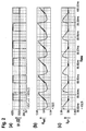
- Fig. 2a shows the input and output voltages
- Fig. 2b shows the input current
- Fig. 2c shows the output diode current waveforms respectively at steady-state operating condition of the converter HBC shown in Fig. 1 .
- the switching on-off scheme of the switching signals S1, S2 is in accordance with a conventional flyback converter concept for the desired output voltage level and is also dependent on the transformer winding turn ratio.
- a detailed operation description of such a conventional Half Bridge Flyback Converter can be found in J.-M. Kwon, W.-Y. Choi, B.-H. Kwon: "High-Performance Plasma-Display-Panel 'Sustain' Power Supply", IEE Proc.-Electr. Power Appl., Vol.152, No.6, November 2005 .
- FIG. 1 and Fig. 2 show the principle block diagram and the operation of a conventional Half Bridge Flyback Converter HBC
- Fig. 1 and Fig. 2 show the principle block diagram and the operation of a conventional Half Bridge Flyback Converter HBC
- several published prior art patent documents disclose drive units for driving such a Half Bridge Flyback Converter HBC.
- US Patent No. 6.639.811 B2 discloses a Half bridge Flyback Converter unit (hereinafter "prior art 1") and its self oscillating switching drive concept in a configuration where the load block is connected in parallel to switching element Q1 instead of switching element Q2 thus interchanging the functions of the switch elements but in principle having the same main operating principle.
- this drive unit both switching elements in the half bridge structure are driven by means of two additional auxiliary winding on the transformer T1 and two separate electronics blocks providing fixed on-time for both the energy storage cycle (when Q1 is on) and the energy transfer cycle (when Q2 is on) without using any controller integrated circuit (IC).
- the principle block diagrams of the disclosed self oscillating power supply unit of "prior art 1" are shown in Fig. 3, Fig. 4 and Fig. 5 .
- Switching power supply units similar to the one in "prior art 1" and including two switching elements in the primary side and a corresponding drive unit are disclosed in US Patent No. 5.796.595 , Japanese Unexamined Patent Application No. 4-87560 and Japanese Unexamined Utility Model Publication No. 6-36392 .
- the disclosed drive concept in these publications is not self oscillating but uses a controller IC of two complementary output drives with a time delay produced within itself.
- the drive unit disclosed in US Patent No. 5.796.595 is shown in Fig. 6 (hereinafter called "prior art 2").
- Half bridge drive units in the form of integrated circuits (Ics) are known under the model numbers L6384 and IR2184 (hereinafter called "prior art 3"). These drive ICs have one input pin and two complementary outputs outputting the complementary switching signals. This type of drive unit IC has its own time delay function between the output drive signals together with isolated ground high side switch drive circuit in one integrated circuit and Fig. 7 shows a principle block diagram of the drive unit IC model number L6384.
- the drive signals are coupled to the transistors via an insulation transformer.
- the switching element S2 is turned off before the energy transfer to the secondary side is fully completed such that there is generated a turn-on voltage at the drive (secondary) winding of the switching element S1.
- This process requires turn-off of the output diode Ds at a current larger than a zero value which increases the output diode switching losses.
- the type of switching power supply unit disclosed in US Patent No. 5.796.595 does not have a self oscillating unit but uses a controller integrated circuit (IC) with two drive outputs with or without a pulse transformer or a single output PWM driver with a Half bridge high side driver of two outputs providing a required time delay between the switching and the drive signal for the high side switching element which is at a different ground level.
- IC controller integrated circuit
- the interrupt of energy transfer to the secondary side is not required, very high prices of this kind of ICs increases the cost enormously.
- the object of the present invention is to provide a drive unit for a half bridge converter and a half bridge converter using such a drive unit such that the novel drive unit is extremely simple in its structure, is cost and size efficient and allows a half-bridge flyback circuit driven by it to be power efficient whilst at the same time having low switching losses.
- each time delay circuit respectively comprises a transistor, a resistor, a capacitor and a diode.
- a diode preferably also contributes to the delay operation and is not used only for protection purposes.
- said drive unit is characterized in that said time delay circuits introduce a respective time delay such that one switching element is switched off completely before the other one switching element switches on.
- said drive unit is characterized in that said each time delay circuit is respectively connected serially at the output terminal of the respective secondary winding.
- said drive unit is characterized in that a first input terminal of said primary winding is connected to ground.
- said drive unit is characterized in that a coupling capacitor is connected to a second input terminal of said primary winding.
- said drive unit is characterized in that a first and second over voltage protection circuit is respectively provided at the output of said first and second time delay circuit for respectively protecting said first and second switching element from over voltages.
- said drive unit is characterized in that said each over voltage protection circuit comprises a number of Zener diodes.
- said drive unit is characterized in that said control pulse signal is a pulse width modulated control pulse signal, said first and second switching pulse signals and said time delayed first and second switching pulse signals are PWM switching signals and said controller is a PWM controller.
- said drive unit is characterized in that said aid PWM controller is a single output voltage mode PWM controller. with a drive unit as defined in claims 1 to 8
- a half bridge converter with a drive unit as defined in claims 1 to 8 for converting a DC input voltage to a DC output voltage comprising a switching stage comprising two serially connected switching elements, an output transformer having a primary winding connected to said switching stage and a secondary winding, a half bridge rectifier connected to said output transformer, said half bridge rectifier outputting said DC output voltage, wherein said first and second time delayed switching pulse signals are fed to a respective control terminal of said first and second switching element of said switching stage of said half bridge converter.
- said half bridge converter is characterized in that said switching elements are constituted by MOSFET transistors.
- said half bridge converter is characterized in that said output transformer is connected to said switching stage through a resonant coupling capacitor.
- said half bridge converter is characterized in that the terminals of said primary winding of said output transformer are respectively connected to a drain and a source of one of said serially connected MOSFETs of said switching stage.
- said half bridge converter is characterized in that said one terminal of said primary winding of said output transformer is connected to the source of one MOSFET of said serially connected MOSFETs, and the second terminal of said primary winding of said output transformer is connected to the drain of said one MOSFET.
- said half bridge converter is characterized in that said half bridge converter (HBC) is a half bridge flyback converter.
- a main advantage achieved by using the inventive drive unit and the half bridge converter using such a drive unit is that the zero current switching of an output diode can be provided in a simple and cost efficient manner in a half bridge flyback converter unit, and a conventional single output PWM controller IC with self time shifting pulse transformer can be used in the half bridge drive unit which also reduces the cost considerably.
- a further advantage is that by using two time delay circuits respectively at the output secondary windings of an output transformer and by providing a self time delay unit over it, both the drive of the high side switch of a half bridge structure and a time delay between the two switching elements can be provided in a very cheap manner without the need to use a half bridge driver IC including a High side drive and time delay properties within itself. Using the time delay circuits a time shift between the two complementary switching operations is guaranteed which reduces the switching losses as will be explained with more details below.
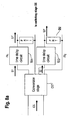
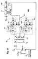
- Fig. 8a shows a principle block diagram of a drive unit DU in accordance with the invention and Figs. 1b-1f serve explanation of the timing related aspects in the drive unit DU of Fig. 8a .
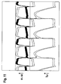
- Fig. 11 shows the switching signals S1, S2 and the output current in the embodiment in Fig. 8a , 8b .
- FIG. 8a a block diagram of a drive unit DU in accordance with the principle of the invention is shown and Fig. 8b shows a special embodiment of the drive unit DU in Fig. 8a .
- the drive unit DU comprises a conversion stage CST, preferably a transformer T2 having a primary winding T2-1 and two secondary windings T2-21, T2-22, said primary winding T2-1 receiving a control pulse signal CS from a controller (not shown in Fig. 8a and Fig. 8b but shown with reference numeral CNTRL in Fig. 9 and Fig. 10 ) and said two secondary windings T2-21, T2-22 outputting a first and second switching pulse signal S1, S2.
- Said first and second switching pulse signals S1, S2 are complementary to each other like the signals S1, S2 discussed above in connection with Fig. 1a and Fig 2 .
- Fig. 8a there is also shown a first and a second time delay circuit TD1, TD2 which respectively receives said first and second complementary switching signal S1, S2.
- Each time delay circuit introduces a respective time delay ⁇ t1, ⁇ t2 in said first and second switching signal S1, S2.
- the first and second time delayed switching pulse signals S1', S2' are then fed to a first and second switching element Q1, Q2, such as a respective MOSFET shown in Fig. 1s, of the switching stage SS of said half bridge converter HBC.
- a first and second over voltage protection circuit PRT1, PRT2 respectively provided at the output of said first and second time delay circuit TD1, TD2 for respectively protecting said first and second switching element Q1, Q2 from over voltages.
- these over voltage protection circuits PRT1, PRT2 can be formed by a number of Zener diodes D3, D4; D5, D6 interconnected as shown in Fig. 8b .
- These Zener diodes shown in the circuit have no particular function in the time delaying/shifting process and they are used just for protection purposes and can be discarded from the circuit. Also other circuit elements can be used instead of them.
- a highly efficient and low cost self time shifting half bridge drive methodology is applied to a general half bridge flyback converter topology.
- half bridge converter structures including two switching elements are very popular especially for medium power levels less than 1kW when compared with full bridge structures with four switching elements because of their simple structure and low cost.
- a half bridge structure (the switching stage SS) consists of two serially connected switching element Q1, Q2 to be switched alternately by the time-delayed switching signals S1', S2'.
- the inventors noticed two main problems, namely that
- the known solutions to these problems are half bridge controller ICs with two time shifted drive signals and pulse transformers for high side driving, totem-pole drive circuits for low voltage applications, or Half bridge high side drive ICs performing both time delay and high side drive in one IC.
- all these solutions increase the cost and size considerably.
- the half bridge drive concept of the present invention overcomes all above mentioned drawbacks in a very simple, cheap and compact manner.
- the possibility that it can be used to drive any half bridge topology is another advantage.
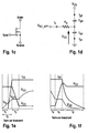
- Fig. 1b shows a principle block diagram of the typical Half Bridge switching structure shown in Fig. 1a where the two switching elements Q1, Q2 connected in series are connected in parallel to the input source Vdc.
- the switching elements Q1, Q2 should never be on simultaneously to prevent the source from being short circuited. Therefore, before opening a switch, the other one must completely be closed, that is a switching time delay should be introduced both when "turning Q1 on-turning Q2 off” and "turning Q1 off -turning Q2 on”. This is the reason for providing - in accordance with the invention - two time delay circuits TD1, TD2.
- Fig. 1c shows the switching element Q1, Q2 formed by MOSFET transistor and Fig. 1d shows the equivalent circuit of Fig. 1c in case of switching, for further illustrating the time delay features of the present invention.
- R g is the internal resistor at the gate terminal
- C gs and C ds are gate source and gate drain capacitances respectively.
- a MOSFET is a voltage controlled switch, in contrary to bipolar transistors and IGBTs which are current controlled switches, and the switching state (on-off) of a MOSFET is determined by the C gs voltage (or gate source voltage).
- Fig. 1e shows typical turn-on and turn-off transients of such a MOSFET.
- V DS voltage stress
- the MOSFET starts to conduct a current I DS when the gate-source voltage V GS reaches a certain threshold value V th and it is completely opened at the end of the so-called "Miller Plateau gate charging process" where V GS stays constant at gate plateau voltage V GP for a certain time t 3 .
- total MOSFET turn-on time is t 2 + t 3 .
- the turning-off process of a MOSFET follows a similar but opposite process as shown in Fig. 1f .
- the total turn-off time can be described as t 4 + t 5 + t 6 .
- These time durations depend on the parameters of the MOSFET used (listed in the data sheets or technical documents) and applied gate-source pulse voltage. Whilst a direct calculation of these turn-on and turn-off time values is extremely complicated they can be estimated roughly by a simple RC circuit analysis, and can be set experimentally afterwards.
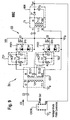
- time delay ⁇ t1, ⁇ t2 provided by the time delay circuits TD1, TD2 is further explained with reference to the special embodiment of a time delay circuit shown in Fig. 8b and comprising a respective diode D1, D2, a resistor R1, R2 and a bipolar transistor T1, T2 and a capacitor C1, C2 interconnected as shown in Fig. 8b (and also shown in Fig. 9 and Fig. 10 ).
- Each time delay circuit TD1, TD2 is respectively connected serially at the output terminal t8, t7 of the respective secondary winding T2-21, T2-22 of the isolation transformer T2.
- the diodes D 1 and D 2 provide a discharge path for the gate-source charge of the corresponding switching MOSFET to be turned-off immediately after the application of a negative pulse voltage, while the part of the time delay circuit TD1, TD2 consisting of the transistor T1, T2, the resistor R1, R2 and the capacitor C1, C2 creates a turn-on time delay for the complementary MOSFET to be turned-on when the complementary positive turn on pulse voltage is applied simultaneously with the turn-off pulse voltage. Furthermore, the turn-on charge path is not available until the base emitter capacitance voltage of the transistor reaches up to a typical threshold value of about 0.65 V.
- this time duration should preferably be at least equal to or greater than the turn-of time (t 4 + t 5 + t 6 ) of the complementary turning-of MOSFET minus the turn-on start time t 1 of the turning-on MOSFET, i.e (t 4 + t 5 + t 6 - t 1 ).
- the collector-emitter capacitor C1, C2 should preferably be kept very small compared to the gate-source capacitor C gs of the used MOSFETs such that when the collector-emitter voltage reaches the threshold of about 0.65 V, the MOSFET gate-source voltage is held at a very small value close to zero to guarantee continuity of the off-state of the MOSFET Q1 while the other MOSFET Q2 is being turned-off.
- the inventive time delay circuits TD1, TD2 advantageously and preferably provide such a time delay as mentioned and discussed above.
- each time delay circuit is respectively connected serially at the respective output terminal t8, t7 of the respective secondary winding T2-21, T2-22.
- Fig. 9 and Fig 10 show embodiments of the drive unit DU of Fig. 8a , 8b respectively employed for driving a half bridge converter HBC such as the one shown and discussed above in connection with Fig. 1a .
- the half bridge converter HBC in Fig. 9 and Fig. 10 is for converting a DC input voltage Vdc to a DC output voltage Vout and it comprises a switching stage Q1, Q2, SS comprising two serially connected switching elements Q1, Q2, preferably MOSFET transistors, an output transformer T1 having a primary winding T11 connected to said switching stage Q1, Q2, SS and a secondary winding T12 and a half bridge rectifier D*, Co connected to said output transformer T1, said half bridge rectifier D*, Co outputting said DC output voltage Vout.
- the drive unit DU as shown in Fig.
- a preferred embodiment of the half-bridge converter HBC is shown with the primary winding T11 connected in parallel over the second switching element Q2, i.e. the terminals t1, t4 of said primary winding T11 of said output transformer T1 are respectively connected to a drain Q2d and a source Q2s of the second switching element Q2 of said serially connected MOSFET transistors Q1, Q2 of said switching stage Q1, Q2, SS.
- a preferred embodiment of the half-bridge converter HBC is shown with the primary winding T11 connected in parallel over the first switching element Q1, i.e. one terminal t1 of said primary winding T11 of said output transformer T1 is connected to the drain Q1d of one MOSFET Q1 of said serially connected MOSFETs Q1, Q2, and the second terminal t4 of said primary winding T11 of said output transformer T1 is connected to the source Q1s of said one MOSFET Q1.
- the half bridge flyback converters HBC in Fig. 9 and Fig. 10 block both include a primary driver unit formed by a controller CNTRL outputting the primary control pulse signal CS to the primary winding T21 of said isolation transformer T2.
- a controller may advantageously be formed by a conventional single output voltage mode PWM controller which outputs a pulse-width modulated (PWM) control signal CS.
- PWM pulse-width modulated
- said control pulse signal CS is a pulse width modulated (PWM) control pulse signal CS
- said first and second switching pulse signals S1, S2 and said time delayed first and second switching pulse signals S1', S2' are also PWM switching signals.
- a second output FB of said PWM controller CNTRL is connected to the output terminal of the half wave rectifier HBR where the converted voltage Vout occurs.
- a first input terminal t11 of said primary winding T21 is connected to ground and the serially connected switching elements Q1 and Q2 are also connected to ground at the source Q2s of the lower switching element Q2. Furthermore, it is advantageous to place a coupling capacitor C3 between the PWM controller CNTRL and the primary winding terminal t2.
- the PWM controller CNTRL In operation of the converter in Fig. 9 and Fig. 10 , the PWM controller CNTRL generates the required PWM signal to drive the respective switching element. In Fig.9 , CNTRL generates the required PWM signal to drive Q1, but in Fig. 10 it generates the required signal to drive Q2. for the power block to perform flyback operation.
- the pulse transformer (transformer) T2 with its two secondary windings T2-21; T2-22 isolates the ground level of the high side switching element Q1 and also transfers the in-phase drive signal for the high side switch and instantly generates the complementary drive signal for the bottom switch switching element Q2.
- the drive unit DU incorporated in the converter HBC in Fig. 9 and Fig. 10 prevents opening of the relevant switch before the close of the other by means of said time delay circuits TD1, TD2) at the output of each secondary winding T2-21, T2-22 of the pulse transformer T2, i.e. of the conversion stage CST.
- each time delay circuit TD1, TD2 is preferably composed of a switching NPN transistor T1, T2, a collector base resistor R1, R2 and a base emitter capacitor C1, C2 which together form the main time shift function, i.e. until the base emitter capacitor charges up to the base emitter threshold voltage the transistor switching element remains closed and does not activate the on-process of the relevant switching element of the respective power block.
- the provision of diodes D1, D2 placed between emitter and collector of the transistors guarantee the start of the switch off-process immediately after the turn-off signal and protect the transistor from high reverse emitter collector voltages.
- a Half bridge Flyback converter stage with its drive unit includes, in a first aspect, two series switching MOSFETS Q1, Q2 in Half bridge structure, a resonating capacitor Cr in series to the primary side T11 of the output transformer T1 such that said primary winding T11 is essentially parallel to the second switching MOSFET Q2, a rectifying diode D* in series to the secondary side T12 of the output transformer T1 and an output bulk capacitor (Co), as the driver unit a single output voltage mode PWM controller CNTRL in series with a DC blocking capacitor C3 and a pulse transformer T2 of two complementary outputs t5-t8 and t6-t7, as one time shifting unit TD1 an NPN transistor T1, a collector base resistor R1, a base emitter capacitor C1 and an emitter collector diode D1 in series with the first output of the pulse transformer t5-t8, a Zener diode D3 and another series but reversely
- a Half bridge Flyback converter stage with its drive unit includes, in a second aspect, two series switching MOSFETS Q1, Q2 in Half bridge structure, a resonating capacitor Cr in series to the primary side T11 of the output transformer T1 such that said primary winding T11 is essentially parallel to the first switching MOSFET Q1, a rectifying diode D* in series to the secondary side T12 of the output transformer T1 and an output bulk capacitor Co as the driver unit a single output voltage mode PWM controller CNTRL in series with a DC blocking capacitorC3 and a pulse transformer T2 of two complementary outputs t5-t8 and t6-t7, as one time shifting unit TD1 an NPN transistor
- T1 a collector base resistor R1, a base emitter capacitor C1 and an emitter collector diode D1 in series with the first output of the pulse transformer t5-t8, a Zener diode D3 and another series but reversely connected Zener diode D4 connected between gate and source of said second switching element Q1, and as another second time shifting unit TD2 an NPN transistor T2, a collector base resistor R2 ,a base emitter capacitor C2 and an emitter collector diode D2 in series to the second output winding T2-22; t6-t7 of the pulse transformer T2, a Zener diode D5 and other series but reversely connected Zener diode D6 connected between gate and source of said second switching element Q2.
Landscapes
- Engineering & Computer Science (AREA)
- Power Engineering (AREA)
- Dc-Dc Converters (AREA)
- Analogue/Digital Conversion (AREA)
Claims (14)
- Antriebseinheit (DU) für Halbbrückenwandler (HBC), umfassend:a) einen Transformator (T2) mit einer Primärwicklung (T2-1) und zwei Sekundärwicklungen (T2-21; T2-22), wobei die Primärwicklung (T2-1) ein Steuerimpulssignal (CS) aus einer Steuerung (CNTRL) empfängt und die zwei Sekundärwicklungen (T2-21, T2-22) ein erstes und ein zweites Umschaltimpulssignal (S1, S2) ausgeben, wobei die ersten und zweiten Umschaltimpulssignale (S1, S2) zueinander komplementär sind; undb) eine erste und zweite Zeitverzögerungsschaltung (TD1, TD2) die jeweils das erste und zweite komplementäre Umschaltsignal (S1, S2) empfangen und eine entsprechende Zeitverzögerung (Δt1; Δt2) in das erste und zweite Umschaltsignal (S1, S2) einführen, wobei die ersten und zweiten zeitverzögerten Umschaltimpulssignale (S1', S2') einem ersten und zweiten Umschaltelemente (Q1, Q2) des Halbbrückenwandlers (HBC) zugeführt werden,
dadurch gekennzeichnet, dass
jede Zeitverzögerungsschaltung (TD1, TD2) jeweils umfasst: einen Transistor (T1, T2), dessen Quelle und Emitter am Ausgangsanschluss (t8, t7) der jeweiligen Sekundärwicklung (T2-21, T2-22) und seinem entsprechenden Umschaltelement (Q1, Q2) verbunden sind; einen Widerstand (R1, R2) und einen Kondensator (C1, C2), der seriell mit dem Widerstand verbunden ist, die parallel mit Quelle und Emitter des Transistors (T1, T2) verbunden sind, dessen Gatter mit der Verbindung zwischen dem Widerstand (R1, R2) und dem Kondensator (C1, C2) verbunden ist, und eine Diode (D1; D2), die parallel mit der Quelle und dem Emitter des Trägersignal (T1, T2) verbunden ist, um einen Entladungspfad für das entsprechende Umschaltelement (Q1, Q2) bereitzustellen. - Antriebseinheit (DU) gemäß Anspruch 1, dadurch gekennzeichnet, dass
die Zeitverzögerungsschaltungen (TD1, TD2) eine entsprechende Zeitverzögerung (Δt1; Δt2) so einführen, dass ein Umschaltelement (Q1) komplett abgeschaltet wird, bevor das andere Umschaltelement (Q2) einschaltet. - Antriebseinheit (DU) gemäß Anspruch 1, dadurch gekennzeichnet, dass
ein erster Eingangsanschluss (t11) der Primärwicklung (T2-1) mit Erde verbunden ist. - Antriebseinheit (DU) gemäß Anspruch 3, dadurch gekennzeichnet, dass
ein Kopplungskondensator (C3) mit einem zweiten Eingangsanschluss (t2) der Primärwicklung (T2-1) verbunden ist. - Antriebseinheit (DU) gemäß Anspruch 1, gekennzeichnet durch
eine erste und zweite Überspannungsschutzschaltung (PRT1, PRT2, D3, D4; D5, D6), die jeweils am Ausgang der ersten und zweiten Zeitverzögerungsschaltung (TD1, TD2) vorgesehen sind, um jeweils die ersten und zweiten Umschaltelemente (Q1, Q2) gegenüber Überspannungen zu schützen. - Antriebseinheit (DU) gemäß Anspruch 5, dadurch gekennzeichnet, dass
jede Überspannungsschutzschaltung (PRT1, PRT2) eine Anzahl von Zenerdioden (D3, D4; D5, D6) umfasst. - Antriebseinheit (DU) gemäß Anspruch 1, dadurch gekennzeichnet, dass
das Steuerimpulssignal (CS) ein Pulsweiten-moduliertes (PWM) Steuerimpulssignal (CS) ist, die ersten und zweiten Umschaltimpulssignale (S1, S2) und zeitverzögerten ersten und zweiten Umschaltimpulssignale (S1', S2') PWM-Umschaltsignale (S1, S2; S1', S2') sind und die Steuerung (CNTRL) eine PWM-Steuerung (CTRL) ist. - Antriebseinheit (DU) gemäß Anspruch 4, dadurch gekennzeichnet, dass
die PWM-Steuerung (CNTRL) eine Einzelausgangsspannungsmodus-PWM-Steuerung (CNTRL) ist. - Halbbrückenwandler (HBC) zum Umwandeln einer Gleichstromeingangsspannung (Vdc) in eine GleichstromAusgangsspannung (Vout), umfassend eine Antriebseinheit (DU) gemäß einem oder mehrerer der Ansprüche 1 bis 8,a) eine Umschaltstufe (Q1, Q2, SS), die zwei seriell verbundene Umschaltelemente (Q1, Q2) umfasst;b) einen Ausgangstransformator (T1) mit einer Primärwicklung (T11), die mit der Umschaltstufe (Q1, Q2, SS) und einer Sekundärwicklung (T12) verbunden ist;c) ein Halbbrückengleichrichter (D*, Co), der mit dem Ausgangstransformator (T1) verbunden ist, wobei der Halbbrückengleichrichter (D*, Co) die Gleichstromausgangsspannung (Vout) ausgibt; undd) die ersten und zweiten zeitverzögerten Umschaltimpulssignale (S1', S2') einem entsprechenden Steueranschluss (Q1b; Q2b des ersten und zweiten Umschaltelementes der Umschaltstufe (A1, Q2, SS) des Halbbrückenwandlers (HBC) zugeführt werden.
- Halbbrückenwandler (HBC) gemäß Anspruch 9, dadurch gekennzeichnet, dass
die Umschaltelemente (Q1, Q2) aus MOSFET-Transistoren aufgebaut sind. - Halbbrückenwandler (HBC) gemäß Anspruch 9, dadurch gekennzeichnet, dass
der Ausgangstransformator (T1) mit der Umschaltstufe (Q1, Q2, SS) über einen resonanten Kopplungskondensator (Cr) verbunden ist. - Halbbrückenwandler (HBC) gemäß Anspruch 10, dadurch gekennzeichnet, dass
die Anschlüsse (t1, t4) der Primärwicklung (T11) des Ausgangstransformators (T1) jeweils mit einem Abfluss (Q2d) und einer Quelle (Q2s) eines (Q2) der seriell verbundenen MOSFETs (Q1, Q2) der Umschaltstufe (Q1, Q2, SS) verbunden sind. - Halbbrückenwandler (HBC) gemäß Anspruch 11, dadurch gekennzeichnet, dass
ein Anschluss (t1) der Primärwicklung (T11) des Ausgangstransformators (T1) mit der Quelle (Q1s) eines MOSFETs (Q1) der seriell verbundenen MOSFETs (Q1, Q2) verbunden ist; und
der zweite Anschluss (t4) der Primärwicklung (T11) des Ausgangstransformators (T1) mit dem Abfluss (Q1s) des einen MOSFET (Q1) verbunden ist. - Halbbrückenwandler (HBC) gemäß Anspruch 9, dadurch gekennzeichnet, dass
der Halbbrückenwandler (HBC) ein Halbbrückensperrwandler ist.
Priority Applications (3)
| Application Number | Priority Date | Filing Date | Title |
|---|---|---|---|
| AT06009555T ATE494656T1 (de) | 2006-05-09 | 2006-05-09 | Treibereinheit für einen halbbrückenumrichter |
| EP06009555A EP1855381B1 (de) | 2006-05-09 | 2006-05-09 | Treibereinheit für einen Halbbrückenumrichter |
| DE602006019385T DE602006019385D1 (de) | 2006-05-09 | 2006-05-09 | Treibereinheit für einen Halbbrückenumrichter |
Applications Claiming Priority (1)
| Application Number | Priority Date | Filing Date | Title |
|---|---|---|---|
| EP06009555A EP1855381B1 (de) | 2006-05-09 | 2006-05-09 | Treibereinheit für einen Halbbrückenumrichter |
Publications (2)
| Publication Number | Publication Date |
|---|---|
| EP1855381A1 EP1855381A1 (de) | 2007-11-14 |
| EP1855381B1 true EP1855381B1 (de) | 2011-01-05 |
Family
ID=37227854
Family Applications (1)
| Application Number | Title | Priority Date | Filing Date |
|---|---|---|---|
| EP06009555A Expired - Lifetime EP1855381B1 (de) | 2006-05-09 | 2006-05-09 | Treibereinheit für einen Halbbrückenumrichter |
Country Status (3)
| Country | Link |
|---|---|
| EP (1) | EP1855381B1 (de) |
| AT (1) | ATE494656T1 (de) |
| DE (1) | DE602006019385D1 (de) |
Families Citing this family (6)
| Publication number | Priority date | Publication date | Assignee | Title |
|---|---|---|---|---|
| US20110101885A1 (en) * | 2009-11-02 | 2011-05-05 | Eric Yang | Led backlight circuit for lcd panels |
| GB2482738B (en) | 2010-08-13 | 2015-05-13 | Nujira Ltd | Switch mode power supply for envelope tracking |
| CN103312132B (zh) * | 2013-07-02 | 2016-04-27 | 上海沪工焊接集团股份有限公司 | 用于逆变焊接电源的驱动电路 |
| CN109935214B (zh) * | 2019-04-24 | 2023-10-20 | 合肥惠科金扬科技有限公司 | 一种背光驱动电路及背光驱动装置 |
| CN114466489B (zh) * | 2020-11-08 | 2024-10-29 | 常德市飞泓光电科技有限公司 | 一种用于多模组路灯的多通道可编程电源 |
| CN115118174A (zh) | 2021-03-09 | 2022-09-27 | 华为数字能源技术有限公司 | 一种非对称半桥反激变换器和电源系统 |
Family Cites Families (2)
| Publication number | Priority date | Publication date | Assignee | Title |
|---|---|---|---|---|
| US5796595A (en) | 1994-02-25 | 1998-08-18 | Astec International Limited | Interleaved continuous flyback power converter system |
| DE10229633A1 (de) * | 2002-07-02 | 2004-01-29 | Patent-Treuhand-Gesellschaft für elektrische Glühlampen mbH | Ansteuerung für einen Halbbrückenwechselrichter |
-
2006
- 2006-05-09 DE DE602006019385T patent/DE602006019385D1/de not_active Expired - Lifetime
- 2006-05-09 AT AT06009555T patent/ATE494656T1/de not_active IP Right Cessation
- 2006-05-09 EP EP06009555A patent/EP1855381B1/de not_active Expired - Lifetime
Also Published As
| Publication number | Publication date |
|---|---|
| ATE494656T1 (de) | 2011-01-15 |
| DE602006019385D1 (de) | 2011-02-17 |
| EP1855381A1 (de) | 2007-11-14 |
Similar Documents
| Publication | Publication Date | Title |
|---|---|---|
| TWI384745B (zh) | 用於交替驅動一半或全橋的閘極驅動器裝置 | |
| Rivas et al. | Design considerations for very high frequency dc-dc converters | |
| KR100691929B1 (ko) | 플로팅 게이트를 가진 동기 정류기에 대한 일반적인 자기 구동 동기 정류 방식 | |
| CN101521459B (zh) | 谐振开关电容直流电压变换器 | |
| US8027179B2 (en) | Inverter circuit and method for operating the inverter circuit | |
| US6839246B1 (en) | Self-driving circuit for a DC/DC converter | |
| US7948775B2 (en) | Duty-cycle-controlled half-bridge resonant converter | |
| US7957161B2 (en) | Power converters | |
| EP1618639B1 (de) | Aktiv-snubber | |
| US7889521B2 (en) | Three-pin integrated synchronous rectifier and a flyback synchronous rectifying circuit | |
| US8724352B2 (en) | Power supply apparatus driving circuit, power supply apparatus driving integrated circuit, and power supply apparatus | |
| EP1266440A1 (de) | Synchrongleichrichtung im sperrwandler | |
| CN101102086B (zh) | 切换驱动电路 | |
| US7400519B2 (en) | Switching power supply | |
| US20040246748A1 (en) | Bridge-buck converter with self-driven synchronous rectifiers | |
| EP1855381A1 (de) | Treibereinheit für einen Halbbrückenumrichter | |
| US8320140B2 (en) | Optimizing operation of DC-to-AC power converter | |
| US7061776B2 (en) | Half-bridge flyback power converter | |
| US7099161B2 (en) | Converter with synchronous rectifier with ZVS | |
| CN114825881B (zh) | 一种llc控制装置 | |
| JP3328671B2 (ja) | 同期整流回路、これを備えたフォワードコンバータおよび同期整流方法 | |
| CN114079368A (zh) | 驱动电路及开关电源装置 | |
| CN116937975A (zh) | 用于双向转换器的电路、双向转换器及其操作方法 | |
| CN100421347C (zh) | 利用推挽式控制芯片驱动双n-mos的半桥式换流电路 | |
| US20070211500A1 (en) | DC-DC converter with direct driven synchronous rectifier |
Legal Events
| Date | Code | Title | Description |
|---|---|---|---|
| PUAI | Public reference made under article 153(3) epc to a published international application that has entered the european phase |
Free format text: ORIGINAL CODE: 0009012 |
|
| AK | Designated contracting states |
Kind code of ref document: A1 Designated state(s): AT BE BG CH CY CZ DE DK EE ES FI FR GB GR HU IE IS IT LI LT LU LV MC NL PL PT RO SE SI SK TR |
|
| AX | Request for extension of the european patent |
Extension state: AL BA HR MK YU |
|
| 17P | Request for examination filed |
Effective date: 20080507 |
|
| 17Q | First examination report despatched |
Effective date: 20080619 |
|
| AKX | Designation fees paid |
Designated state(s): AT BE BG CH CY CZ DE DK EE ES FI FR GB GR HU IE IS IT LI LT LU LV MC NL PL PT RO SE SI SK TR |
|
| RIC1 | Information provided on ipc code assigned before grant |
Ipc: H03K 17/691 20060101ALI20100527BHEP Ipc: H03K 17/284 20060101ALI20100527BHEP Ipc: H02M 1/38 20070101AFI20100527BHEP |
|
| GRAP | Despatch of communication of intention to grant a patent |
Free format text: ORIGINAL CODE: EPIDOSNIGR1 |
|
| GRAS | Grant fee paid |
Free format text: ORIGINAL CODE: EPIDOSNIGR3 |
|
| GRAA | (expected) grant |
Free format text: ORIGINAL CODE: 0009210 |
|
| AK | Designated contracting states |
Kind code of ref document: B1 Designated state(s): AT BE BG CH CY CZ DE DK EE ES FI FR GB GR HU IE IS IT LI LT LU LV MC NL PL PT RO SE SI SK TR |
|
| REG | Reference to a national code |
Ref country code: GB Ref legal event code: FG4D |
|
| REG | Reference to a national code |
Ref country code: CH Ref legal event code: EP |
|
| REG | Reference to a national code |
Ref country code: IE Ref legal event code: FG4D |
|
| REF | Corresponds to: |
Ref document number: 602006019385 Country of ref document: DE Date of ref document: 20110217 Kind code of ref document: P |
|
| REG | Reference to a national code |
Ref country code: DE Ref legal event code: R096 Ref document number: 602006019385 Country of ref document: DE Effective date: 20110217 |
|
| REG | Reference to a national code |
Ref country code: NL Ref legal event code: VDEP Effective date: 20110105 |
|
| PG25 | Lapsed in a contracting state [announced via postgrant information from national office to epo] |
Ref country code: SI Free format text: LAPSE BECAUSE OF FAILURE TO SUBMIT A TRANSLATION OF THE DESCRIPTION OR TO PAY THE FEE WITHIN THE PRESCRIBED TIME-LIMIT Effective date: 20110105 |
|
| LTIE | Lt: invalidation of european patent or patent extension |
Effective date: 20110105 |
|
| PG25 | Lapsed in a contracting state [announced via postgrant information from national office to epo] |
Ref country code: LV Free format text: LAPSE BECAUSE OF FAILURE TO SUBMIT A TRANSLATION OF THE DESCRIPTION OR TO PAY THE FEE WITHIN THE PRESCRIBED TIME-LIMIT Effective date: 20110105 Ref country code: ES Free format text: LAPSE BECAUSE OF FAILURE TO SUBMIT A TRANSLATION OF THE DESCRIPTION OR TO PAY THE FEE WITHIN THE PRESCRIBED TIME-LIMIT Effective date: 20110416 Ref country code: SE Free format text: LAPSE BECAUSE OF FAILURE TO SUBMIT A TRANSLATION OF THE DESCRIPTION OR TO PAY THE FEE WITHIN THE PRESCRIBED TIME-LIMIT Effective date: 20110105 Ref country code: IS Free format text: LAPSE BECAUSE OF FAILURE TO SUBMIT A TRANSLATION OF THE DESCRIPTION OR TO PAY THE FEE WITHIN THE PRESCRIBED TIME-LIMIT Effective date: 20110505 Ref country code: PT Free format text: LAPSE BECAUSE OF FAILURE TO SUBMIT A TRANSLATION OF THE DESCRIPTION OR TO PAY THE FEE WITHIN THE PRESCRIBED TIME-LIMIT Effective date: 20110505 Ref country code: LT Free format text: LAPSE BECAUSE OF FAILURE TO SUBMIT A TRANSLATION OF THE DESCRIPTION OR TO PAY THE FEE WITHIN THE PRESCRIBED TIME-LIMIT Effective date: 20110105 Ref country code: GR Free format text: LAPSE BECAUSE OF FAILURE TO SUBMIT A TRANSLATION OF THE DESCRIPTION OR TO PAY THE FEE WITHIN THE PRESCRIBED TIME-LIMIT Effective date: 20110406 |
|
| PG25 | Lapsed in a contracting state [announced via postgrant information from national office to epo] |
Ref country code: PL Free format text: LAPSE BECAUSE OF FAILURE TO SUBMIT A TRANSLATION OF THE DESCRIPTION OR TO PAY THE FEE WITHIN THE PRESCRIBED TIME-LIMIT Effective date: 20110105 Ref country code: FI Free format text: LAPSE BECAUSE OF FAILURE TO SUBMIT A TRANSLATION OF THE DESCRIPTION OR TO PAY THE FEE WITHIN THE PRESCRIBED TIME-LIMIT Effective date: 20110105 Ref country code: AT Free format text: LAPSE BECAUSE OF FAILURE TO SUBMIT A TRANSLATION OF THE DESCRIPTION OR TO PAY THE FEE WITHIN THE PRESCRIBED TIME-LIMIT Effective date: 20110105 Ref country code: BG Free format text: LAPSE BECAUSE OF FAILURE TO SUBMIT A TRANSLATION OF THE DESCRIPTION OR TO PAY THE FEE WITHIN THE PRESCRIBED TIME-LIMIT Effective date: 20110405 Ref country code: BE Free format text: LAPSE BECAUSE OF FAILURE TO SUBMIT A TRANSLATION OF THE DESCRIPTION OR TO PAY THE FEE WITHIN THE PRESCRIBED TIME-LIMIT Effective date: 20110105 Ref country code: CY Free format text: LAPSE BECAUSE OF FAILURE TO SUBMIT A TRANSLATION OF THE DESCRIPTION OR TO PAY THE FEE WITHIN THE PRESCRIBED TIME-LIMIT Effective date: 20110105 Ref country code: NL Free format text: LAPSE BECAUSE OF FAILURE TO SUBMIT A TRANSLATION OF THE DESCRIPTION OR TO PAY THE FEE WITHIN THE PRESCRIBED TIME-LIMIT Effective date: 20110105 |
|
| REG | Reference to a national code |
Ref country code: DE Ref legal event code: R082 Ref document number: 602006019385 Country of ref document: DE |
|
| PG25 | Lapsed in a contracting state [announced via postgrant information from national office to epo] |
Ref country code: EE Free format text: LAPSE BECAUSE OF FAILURE TO SUBMIT A TRANSLATION OF THE DESCRIPTION OR TO PAY THE FEE WITHIN THE PRESCRIBED TIME-LIMIT Effective date: 20110105 Ref country code: DK Free format text: LAPSE BECAUSE OF FAILURE TO SUBMIT A TRANSLATION OF THE DESCRIPTION OR TO PAY THE FEE WITHIN THE PRESCRIBED TIME-LIMIT Effective date: 20110105 |
|
| PLBE | No opposition filed within time limit |
Free format text: ORIGINAL CODE: 0009261 |
|
| STAA | Information on the status of an ep patent application or granted ep patent |
Free format text: STATUS: NO OPPOSITION FILED WITHIN TIME LIMIT |
|
| PG25 | Lapsed in a contracting state [announced via postgrant information from national office to epo] |
Ref country code: RO Free format text: LAPSE BECAUSE OF FAILURE TO SUBMIT A TRANSLATION OF THE DESCRIPTION OR TO PAY THE FEE WITHIN THE PRESCRIBED TIME-LIMIT Effective date: 20110105 Ref country code: SK Free format text: LAPSE BECAUSE OF FAILURE TO SUBMIT A TRANSLATION OF THE DESCRIPTION OR TO PAY THE FEE WITHIN THE PRESCRIBED TIME-LIMIT Effective date: 20110105 Ref country code: CZ Free format text: LAPSE BECAUSE OF FAILURE TO SUBMIT A TRANSLATION OF THE DESCRIPTION OR TO PAY THE FEE WITHIN THE PRESCRIBED TIME-LIMIT Effective date: 20110105 |
|
| 26N | No opposition filed |
Effective date: 20111006 |
|
| PG25 | Lapsed in a contracting state [announced via postgrant information from national office to epo] |
Ref country code: MC Free format text: LAPSE BECAUSE OF NON-PAYMENT OF DUE FEES Effective date: 20110531 Ref country code: IT Free format text: LAPSE BECAUSE OF FAILURE TO SUBMIT A TRANSLATION OF THE DESCRIPTION OR TO PAY THE FEE WITHIN THE PRESCRIBED TIME-LIMIT Effective date: 20110105 |
|
| REG | Reference to a national code |
Ref country code: CH Ref legal event code: PL |
|
| GBPC | Gb: european patent ceased through non-payment of renewal fee |
Effective date: 20110509 |
|
| PG25 | Lapsed in a contracting state [announced via postgrant information from national office to epo] |
Ref country code: LI Free format text: LAPSE BECAUSE OF NON-PAYMENT OF DUE FEES Effective date: 20110531 Ref country code: CH Free format text: LAPSE BECAUSE OF NON-PAYMENT OF DUE FEES Effective date: 20110531 |
|
| REG | Reference to a national code |
Ref country code: DE Ref legal event code: R097 Ref document number: 602006019385 Country of ref document: DE Effective date: 20111006 |
|
| REG | Reference to a national code |
Ref country code: FR Ref legal event code: ST Effective date: 20120131 |
|
| REG | Reference to a national code |
Ref country code: IE Ref legal event code: MM4A |
|
| PG25 | Lapsed in a contracting state [announced via postgrant information from national office to epo] |
Ref country code: IE Free format text: LAPSE BECAUSE OF NON-PAYMENT OF DUE FEES Effective date: 20110509 Ref country code: FR Free format text: LAPSE BECAUSE OF NON-PAYMENT OF DUE FEES Effective date: 20110531 |
|
| PG25 | Lapsed in a contracting state [announced via postgrant information from national office to epo] |
Ref country code: GB Free format text: LAPSE BECAUSE OF NON-PAYMENT OF DUE FEES Effective date: 20110509 |
|
| PG25 | Lapsed in a contracting state [announced via postgrant information from national office to epo] |
Ref country code: LU Free format text: LAPSE BECAUSE OF NON-PAYMENT OF DUE FEES Effective date: 20110509 |
|
| PG25 | Lapsed in a contracting state [announced via postgrant information from national office to epo] |
Ref country code: HU Free format text: LAPSE BECAUSE OF FAILURE TO SUBMIT A TRANSLATION OF THE DESCRIPTION OR TO PAY THE FEE WITHIN THE PRESCRIBED TIME-LIMIT Effective date: 20110105 |
|
| PGFP | Annual fee paid to national office [announced via postgrant information from national office to epo] |
Ref country code: DE Payment date: 20200520 Year of fee payment: 15 |
|
| REG | Reference to a national code |
Ref country code: DE Ref legal event code: R119 Ref document number: 602006019385 Country of ref document: DE |
|
| PG25 | Lapsed in a contracting state [announced via postgrant information from national office to epo] |
Ref country code: DE Free format text: LAPSE BECAUSE OF NON-PAYMENT OF DUE FEES Effective date: 20211201 |
|
| PGFP | Annual fee paid to national office [announced via postgrant information from national office to epo] |
Ref country code: TR Payment date: 20250507 Year of fee payment: 20 |