EP1857575A2 - Complexe métal-nanocristal semi-conducteur et son procédé de préparation - Google Patents
Complexe métal-nanocristal semi-conducteur et son procédé de préparation Download PDFInfo
- Publication number
- EP1857575A2 EP1857575A2 EP07103276A EP07103276A EP1857575A2 EP 1857575 A2 EP1857575 A2 EP 1857575A2 EP 07103276 A EP07103276 A EP 07103276A EP 07103276 A EP07103276 A EP 07103276A EP 1857575 A2 EP1857575 A2 EP 1857575A2
- Authority
- EP
- European Patent Office
- Prior art keywords
- semiconductor nanocrystal
- metal
- metal complex
- semiconductor
- nanocrystal
- Prior art date
- Legal status (The legal status is an assumption and is not a legal conclusion. Google has not performed a legal analysis and makes no representation as to the accuracy of the status listed.)
- Withdrawn
Links
Images


Classifications
-
- C—CHEMISTRY; METALLURGY
- C30—CRYSTAL GROWTH
- C30B—SINGLE-CRYSTAL GROWTH; UNIDIRECTIONAL SOLIDIFICATION OF EUTECTIC MATERIAL OR UNIDIRECTIONAL DEMIXING OF EUTECTOID MATERIAL; REFINING BY ZONE-MELTING OF MATERIAL; PRODUCTION OF A HOMOGENEOUS POLYCRYSTALLINE MATERIAL WITH DEFINED STRUCTURE; SINGLE CRYSTALS OR HOMOGENEOUS POLYCRYSTALLINE MATERIAL WITH DEFINED STRUCTURE; AFTER-TREATMENT OF SINGLE CRYSTALS OR A HOMOGENEOUS POLYCRYSTALLINE MATERIAL WITH DEFINED STRUCTURE; APPARATUS THEREFOR
- C30B7/00—Single-crystal growth from solutions using solvents which are liquid at normal temperature, e.g. aqueous solutions
-
- B—PERFORMING OPERATIONS; TRANSPORTING
- B82—NANOTECHNOLOGY
- B82B—NANOSTRUCTURES FORMED BY MANIPULATION OF INDIVIDUAL ATOMS, MOLECULES, OR LIMITED COLLECTIONS OF ATOMS OR MOLECULES AS DISCRETE UNITS; MANUFACTURE OR TREATMENT THEREOF
- B82B3/00—Manufacture or treatment of nanostructures by manipulation of individual atoms or molecules, or limited collections of atoms or molecules as discrete units
-
- B—PERFORMING OPERATIONS; TRANSPORTING
- B82—NANOTECHNOLOGY
- B82Y—SPECIFIC USES OR APPLICATIONS OF NANOSTRUCTURES; MEASUREMENT OR ANALYSIS OF NANOSTRUCTURES; MANUFACTURE OR TREATMENT OF NANOSTRUCTURES
- B82Y15/00—Nanotechnology for interacting, sensing or actuating, e.g. quantum dots as markers in protein assays or molecular motors
-
- B—PERFORMING OPERATIONS; TRANSPORTING
- B82—NANOTECHNOLOGY
- B82Y—SPECIFIC USES OR APPLICATIONS OF NANOSTRUCTURES; MEASUREMENT OR ANALYSIS OF NANOSTRUCTURES; MANUFACTURE OR TREATMENT OF NANOSTRUCTURES
- B82Y30/00—Nanotechnology for materials or surface science, e.g. nanocomposites
-
- C—CHEMISTRY; METALLURGY
- C30—CRYSTAL GROWTH
- C30B—SINGLE-CRYSTAL GROWTH; UNIDIRECTIONAL SOLIDIFICATION OF EUTECTIC MATERIAL OR UNIDIRECTIONAL DEMIXING OF EUTECTOID MATERIAL; REFINING BY ZONE-MELTING OF MATERIAL; PRODUCTION OF A HOMOGENEOUS POLYCRYSTALLINE MATERIAL WITH DEFINED STRUCTURE; SINGLE CRYSTALS OR HOMOGENEOUS POLYCRYSTALLINE MATERIAL WITH DEFINED STRUCTURE; AFTER-TREATMENT OF SINGLE CRYSTALS OR A HOMOGENEOUS POLYCRYSTALLINE MATERIAL WITH DEFINED STRUCTURE; APPARATUS THEREFOR
- C30B29/00—Single crystals or homogeneous polycrystalline material with defined structure characterised by the material or by their shape
- C30B29/60—Single crystals or homogeneous polycrystalline material with defined structure characterised by the material or by their shape characterised by shape
-
- B—PERFORMING OPERATIONS; TRANSPORTING
- B82—NANOTECHNOLOGY
- B82Y—SPECIFIC USES OR APPLICATIONS OF NANOSTRUCTURES; MEASUREMENT OR ANALYSIS OF NANOSTRUCTURES; MANUFACTURE OR TREATMENT OF NANOSTRUCTURES
- B82Y40/00—Manufacture or treatment of nanostructures
Definitions
- the present invention relates to a semiconductor nanocrystal-metal complex and a method for preparing the complex. More specifically, the present invention relates to a semiconductor nanocrystal-metal complex having a semiconductor nanocrystal and one or more metal particles bound to the surface of the semiconductor nanocrystal, and a method for preparing the semiconductor nanocrystal-metal complex.
- a semiconductor nanocrystal (also referred to as a "quantum dot”) is defined as a crystalline material having a size on the order of a few nanometers, and includes about several hundred to about several thousand atoms. Since a small-sized semiconductor crystal has a large surface area per unit volume, most of the constituent atoms of the nanocrystal are present on the surface of the nanocrystal. Based on this characteristic structure, a semiconductor nanocrystal exhibits a quantum confinement effect and exhibits electrical, magnetic, optical, chemical and mechanical properties different from those inherent to the constituent atoms of the nanocrystal. That is, control over the physical size of semiconductor nanocrystals enables the control of the properties of the nanocrystals. Devices, such as displays and biological probes, using various characteristics of semiconductor nanocrystals, are currently being developed.
- one electronic device such as a light-emitting diode (LED)
- a semiconductor nanocrystal as a light-emitting material.
- a process for treating a material using a semiconductor nanocrystal probe includes determining the presence of a biological substance in the material wherein the semiconductor nanocrystal probe is formed by sequentially linking one or more linking agents and one or more affinity molecules to semiconductor nanocrystals.
- the present invention has been made in view of the above problems, and one aspect of the present invention includes providing a semiconductor nanocrystal-metal complex that can vary the characteristics of a semiconductor nanocrystal and has improved reactivity.
- Another aspect of the present invention includes providing a method for preparing a semiconductor nanocrystal-metal complex that can be performed at room temperature without using an additional apparatus or involving any complicated steps.
- a semiconductor nanocrystal-metal complex includes a semiconductor nanocrystal and one or more metal particles bound to the semiconductor nanocrystal.
- a method for preparing a semiconductor nanocrystal-metal complex includes preparing a semiconductor nanocrystal and mixing the semiconductor nanocrystal with a metal precursor and reducing the metal precursor into metal particles to allow the metal particles to bind to the semiconductor nanocrystal.
- first, second, third etc. may be used herein to describe various elements, components, regions, layers and/or sections, these elements, components, regions, layers and/or sections should not be limited by these terms. These terms are only used to distinguish one element, component, region, layer or section from another element, component, region, layer or section. Thus, a first element, component, region, layer or section discussed below could be termed a second element, component, region, layer or section without departing from the teachings of the present invention.
- spatially relative terms such as “beneath”, “below”, “lower”, “above”, “upper” and the like, may be used herein for ease of description to describe one element or feature's relationship to another element(s) or feature(s) as illustrated in the figures. It will be understood that the spatially relative terms are intended to encompass different orientations of the device in use or operation in addition to the orientation depicted in the figures. For example, if the device in the figures is turned over, elements described as “below” or “beneath” other elements or features would then be oriented “above” the other elements or features. Thus, the exemplary term “below” can encompass both an orientation of above and below. The device may be otherwise oriented (rotated 90 degrees or at other orientations) and the spatially relative descriptors used herein interpreted accordingly.
- the present invention is directed to a semiconductor nanocrystal-metal complex in which metal particles are bound to a semiconductor nanocrystal.
- the semiconductor nanocrystal-metal complex comprises a semiconductor nanocrystal and one or more metal particles bound to the surface of the semiconductor nanocrystal.
- the metal particles may be directly bound to the surface of the semiconductor nanocrystal.
- the semiconductor nanocrystal may have various shapes, including that of a sphere, tetrahedron, cylinder, rod, triangle, disc, tripod, tetrapod, cube, box, star, tube, or the like.
- the metal particles can be bound to the semiconductor nanocrystal at various positions without restriction. For example, the metal particles may be bound to the edges or ends of the semiconductor nanocrystal.
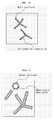
- FIGS. 1a to 1c Various exemplary embodiments of structures of semiconductor nanocrystal-metal complexes according to the present invention are shown in FIGS. 1a to 1c.
- FIG. 1a is a schematic diagram showing exemplary embodiments of structures of semiconductor nanocrystal-metal complexes in which the semiconductor nanocrystals are spherical. According to the nanocrystal-metal complexes of the embodiments shown in FIG. 1a, one or more metal particles are bound to the surface edges of the spherical semiconductor nanocrystals.
- FIG. 1b is a schematic diagram showing exemplary embodiments of structures of semiconductor nanocrystal-metal complexes in which the semiconductor nanocrystals are rod-shaped
- FIG. 1c is a schematic diagram showing exemplary embodiments of structures of semiconductor nanocrystal-metal complexes in which the semiconductor nanocrystals have tripod and tetrapod shapes.
- nanocrystal-metal complexes having a dendritic form i.e. a tripod or tetrapod
- metal particles are bound to the ends of the semiconductor nanocrystals.
- the semiconductor nanocrystal-metal complex thus prepared can have a core-shell structure.
- the semiconductor nanocrystal-metal complexes include a core formed from the semiconductor nanocrystal having various shapes (including spheres, rods and tetrapods, and the like) and a shell formed from the metal particles to surround the core.
- any semiconductor that exhibits a quantum confinement effect may be used to form the semiconductor nanocrystal of the semiconductor nanocrystal-metal complex.
- the semiconductor may be selected from the group consisting of Group II-VI, Group III-V, Group IV-VI, and Group IV semiconductor compounds, and mixtures thereof.
- CdS, CdSe, CdTe, ZnS, ZnSe, ZnTe, HgS, HgSe, HgTe, PbS, PbSe, PbTe, AlN, AlP, AlAs, GaN, GaP, GaAs, InN, InP, InAs, or a mixture thereof can be used to form the semiconductor nanocrystal.
- metal used to make the metal particles is not specifically limited so long as it can be bound to the surface of the nanocrystal.
- the metal can be selected from the group consisting of Au, Ag, Cu, Pt, Pd, Ni, Fe and Co particles.
- the metal particles may be metal nanoparticles having a size of about several nanometers to about several tens of nanometers.
- the semiconductor nanocrystal-metal complex of the present invention exhibits excellent photocurrent characteristics, and is easy to prepare even at room temperature without involving complicated steps.
- the semiconductor nanocrystal-metal complex of the present invention exhibits both characteristics of the semiconductor nanostructure and characteristics of the metal nanostructure, thus permitting transition of electrons excited to quantized energy levels to the metal nanostructure, which causes a resonance phenomenon to occur. That is, the semiconductor nanocrystal-metal complex of the present invention exhibits new characteristics other than characteristics of the semiconductor nanostructure and the metal nanostructure.
- the luminescent properties of the semiconductor nanocrystal-metal complex according to the present invention may disappear or be weakened, unlike those of semiconductor nanocrystals, as determined by photoluminescence spectroscopy. It is assumed that the reason for this disappearance or weakening of the luminescent properties is that less recombination of excitons takes place and instead charge separation occurs within the semiconductor nanocrystal-metal complex, or that Auger recombination of the semiconductor nanocrystal is induced due to the metal structure.
- the semiconductor nanocrystal-metal complex of the present invention can be used to manufacture of a variety of devices, (e.g., solar cells, optical sensors, and the like), using photocurrent characteristics.
- the metal particles bound to the semiconductor nanocrystal of the semiconductor nanocrystal-metal complex according to the present invention can easily form strong covalent bonds with organic materials having a functional group, thus enabling the application of the semiconductor nanocrystal-metal complex in arrays that can utilize the characteristics of the semiconductor nanocrystal. Therefore, the semiconductor nanocrystal-metal complex of the present invention can find application in various fields, including bioassays.
- the method for preparing the semiconductor nanocrystal-metal complex comprises preparing a semiconductor nanocrystal and mixing the semiconductor nanocrystal with a metal precursor and reducing the metal precursor into metal particles to allow the metal particles to bind to the semiconductor nanocrystal.
- the semiconductor nanocrystal can be synthesized from precursors containing constituent elements of the semiconductor nanocrystal by any synthetic process.
- the semiconductor nanocrystal can be synthesized by mixing a metal precursor and a chalcogenide precursor in a solvent and a dispersant, and heating the mixture with uniform stirring under an inert atmosphere to react the metal precursor with the chalcogenide precursor.
- a single compound containing a metal and a chalcogenide element may be added instead of the metal precursor and the chalcogenide precursor.
- the shape of the semiconductor crystal may be controlled by varying the concentration of the precursors, the reaction temperature, the kind of the dispersant used, and the like.
- metal precursors that can be used in preparing a semiconductor nanocrystal include, but are not limited to, dimethyl zinc, diethyl zinc, zinc acetate, zinc acetylacetonate, zinc iodide, zinc bromide, zinc chloride, zinc fluoride, zinc carbonate, zinc cyanide, zinc nitrate, zinc oxide, zinc peroxide, zinc perchlorate, zinc sulfate, dimethyl cadmium, diethyl cadmium, cadmium acetate, cadmium acetylacetonate, cadmium iodide, cadmium bromide, cadmium chloride, cadmium fluoride, cadmium carbonate, cadmium nitrate, cadmium oxide, cadmium perchlorate, cadmium phosphide, cadmium sulfate, mercury acetate, mercury
- chalcogenide precursors that can be used in preparing the semiconductor nanocrystal, where a metal precursor and a chalcogenide precursor are used, include, but are not limited to, alkanethiol compounds (e.g., hexane thiol, octane thiol, decane thiol, dodecane thiol, hexadecane thiol, octadecane thiol and mercaptopropyl silane), sulfur-trioctylphosphine (S-TOP), sulfur-tributylphosphine (S-TBP), sulfur-triphenylphosphine (S-TPP), sulfur-trioctylamine (S-TOA), trimethylsilyl sulfur, ammonium sulfide, sodium sulfide, selenium-trioctylphosphine (Se-TOP), selenium-tributylphosphine
- Examples of dispersants that can be used in preparing the semiconductor nanocrystal include C 6 -C 22 alkanes and alkenes having a terminal carboxyl (COOH) group; C 6 -C 22 alkanes and alkenes having a terminal phosphoryl (POOH) group; C 6 -C 22 alkanes and alkenes having a terminal sulfhydryl (SOOH) group; and C 6 -C 22 alkanes and alkenes having a terminal amino (-NH 2 ) group.
- COOH carboxyl
- POOH phosphoryl
- SOOH sulfhydryl
- oleic acid stearic acid, palmitic acid, hexylphosphonic acid, n-octylphosphonic acid, tetradecylphosphonic acid, octadecylphosphonic acid, n-octyl amine, or hexadecyl amine can be used.
- step (b) first, the semiconductor nanocrystal is mixed with a metal precursor. Thereafter, the metal precursor is reduced into metal particles to allow the metal particles to bind to the semiconductor nanocrystal.
- the metal precursor used in the mixing step can be prepared by dissolving an organic solvent-soluble organometallic complex containing a metal, which is the same species as the metal of the metal precursor, in a solvent and a dispersant.
- the metal necessary for the formation of the metal precursor is not particularly limited so long as it can be bound to the surface of the nanocrystal.
- the metal can be selected from the group consisting of Au, Ag, Cu, Pt, Pd, Ni, Fe, and Co.
- suitable organometallic complexes containing the metal include ammonium tetrachloroaurate, hydrogen tetrabromoaurate, hydrogen tetrachloroaurate, potassium dicyanoaurate, potassium tetrabromoaurate, potassium tetrachloroaurate, sodium tetrabromoaurate, di-n-butyltin dilaurate, silver acetate, silver bromide, silver carbonate, silver chloride, silver chromate, silver cyanide, silver cyclohexanebutyrate, silver 2-ethylhexanoate, silver (I) fluoride, silver (II) fluoride, silver hexabromocarborane, silver hexafluoroantimonate, silver hexafluoroarsenate, silver hexafluorophosphate, silver iodide, silver nitrate, silver perchlorate, silver perchlorate monohydrate, silver perrhenate, silver
- dispersant used for the formation of the metal precursor in the mixing step is not limited, but exemplary dispersants can be selected from the group consisting of oleic acid, stearic acid, palmitic acid, hexylphosphonic acid, n-octylphosphonic acid, tetradecylphosphonic acid, octadecylphosphonic acid, trioctylphosphine, trioctylphosphine oxide, n-octyl amine, hexadecyl amine, hexane thiol, octane thiol, and octadecane thiol.
- the reduction of the metal precursor can be achieved by adding the semiconductor nanocrystal solution prepared in the previous step to the metal precursor solution, followed by stirring for a given time.
- the reaction temperature is not critical. Since the reaction occurs even at room temperature, the semiconductor nanocrystal-metal complex of the present invention can be sufficiently prepared without heating.
- metal particles are bound to the surface of the semiconductor nanocrystal. There is no restriction on where the metal particles can be bound to the semiconductor nanocrystal. For example, the metal particles may be preferentially bound to the sharp edges or ends of the semiconductor nanocrystal, as shown in FIGs. 1a to 1c.
- the concentration and kind of the metal precursor and the reaction temperature are varied so that the metal precursor can be reduced into metal particles in large quantities to form a continuous or discrete layer on the surface of the semiconductor nanocrystal.
- the semiconductor nanocrystal-metal complex thus prepared comprises a core formed of the semiconductor nanocrystal and a shell formed of the metal particles. Exemplary embodiments of structures of core-shell type semiconductor nanocrystal-metal complexes according to the present invention are shown in FIG. 2.
- Example 1 Synthesis of spherical semiconductor nanocrystal-metal (CdSeS/Au) complex
- TOA trioctylamine
- oleic acid about 0.5 g of oleic acid and about 0.4 millimoles (mmol) of cadmium oxide
- the reaction temperature of the mixture was adjusted to about 300 degrees Celsius (°C) with stirring to prepare a cadmium precursor solution.
- a selenium (Se) powder was dissolved in trioctylphosphine (TOP) to obtain an approximately 1 molar (M) Se-TOP complex solution
- S sulfur
- a mixture of about 0.5 ml of the S-TOP complex solution and about 0.5 ml of the Se-TOP complex solution was rapidly fed to the cadmium precursor solution, followed by stirring for about 4 minutes to form a CdSeS nanocrystal or quantum dot (QD).
- QD quantum dot
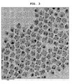
- FIG. 3 shows a transmission electron microscope (TEM) image of the semiconductor nanocrystal-metal (CdSeS/Au) complex. The TEM image demonstrated that one or more metal particles were bound to the surface of the spherical semiconductor nanocrystal.
- TOPO trioctylphosphine oxide
- octadecylphosphonic acid about 0.205 g
- cadmium oxide about 0.205 g
- the reaction temperature of the mixture was adjusted to about 330°C with stirring to prepare a cadmium precursor solution.
- a selenium (Se) powder about 0.23 ml of tributylphosphine (TBT), about 1.74 ml of TOP and about 0.3 ml of toluene were mixed to obtain a Se complex solution. While the Se complex solution was fed to the cadmium precursor solution, the reaction temperature was lowered to about 280°C. The reaction mixture was stirred for about 6 minutes to form a bar-shaped CdSe nanocrystal.
- FIG. 4 is a TEM image of the semiconductor nanocrystal-metal (CdSe/Au) complex.
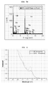
- FIG. 5a is a scanning transmission electron microscope (STEM) image of the semiconductor nanocrystal-metal complex
- FIG. 5b is an energy dispersive X-ray spectroscopy (EDS) spectrum of the semiconductor nanocrystal-metal complex.
- the spectrum of FIG. 5b indicates that Cd, Se and Au elements were detected from the semiconductor nanocrystal-metal complex.
- the characteristics of the spherical semiconductor nanocrystal-metal complex prepared in Example 1 were evaluated. After the spherical semiconductor nanocrystal-metal complex and the semiconductor nanocrystal quantum dot (QD) prepared in Example 1 were prepared, they were cooled to room temperature as rapidly as possible. Ethanol as a non-solvent was separately added to the nanocrystal-metal complex and the nanocrystal, and the resulting mixtures were centrifuged.
- QD semiconductor nanocrystal quantum dot
- the obtained precipitates were separated from the respective supernatants, and dispersed in toluene to prepare an about 1 wt% solution of the CdSeS nanocrystal and an about 1 wt% solution of the semiconductor nanocrystal-metal (CdSeS/Au) complex.
- FIGS. 6 and 7 are absorption spectra and photoluminescence spectra of the CdSeS nanocrystal solution and the semiconductor nanocrystal-metal (CdSeS/Au) complex solution, respectively.
- the characteristics of the bar-shaped semiconductor nanocrystal-metal complex prepared in Example 2 were evaluated. After the bar-shaped semiconductor nanocrystal-metal complex and the semiconductor nanocrystal prepared in Example 2 were prepared, they were cooled to room temperature as rapidly as possible. Ethanol as a non-solvent was separately added to the nanocrystal-metal complex and the nanocrystal, and the resulting mixtures were centrifuged. The obtained precipitates were separated from the respective supernatants, and dispersed in toluene to prepare an about 1 wt% solution of the CdSe nanocrystal and an about 1 wt% solution of the semiconductor nanocrystal-metal (CdSe/Au) semiconductor complex.
- FIG. 8 includes absorption spectra of the CdSe nanocrystal solution and the semiconductor nanocrystal-metal (CdSe/Au) complex solution.
- the semiconductor nanocrystal-metal complex of the present invention exhibits both characteristics of a semiconductor and characteristics of a metal, it exhibits excellent photocurrent characteristics. Owing to the presence of metal particles bound to the semiconductor nanocrystal, the binding force between the semiconductor nanocrystal and other materials is improved, thus broadening the applicability of the semiconductor nanocrystal.
- the semiconductor nanocrystal-metal complex can be easily prepared even at room temperature without using additional equipment or involving complicated steps.
Landscapes
- Chemical & Material Sciences (AREA)
- Engineering & Computer Science (AREA)
- Crystallography & Structural Chemistry (AREA)
- Nanotechnology (AREA)
- Materials Engineering (AREA)
- Organic Chemistry (AREA)
- Metallurgy (AREA)
- Health & Medical Sciences (AREA)
- Molecular Biology (AREA)
- General Health & Medical Sciences (AREA)
- Life Sciences & Earth Sciences (AREA)
- Physics & Mathematics (AREA)
- Composite Materials (AREA)
- Condensed Matter Physics & Semiconductors (AREA)
- General Physics & Mathematics (AREA)
- Manufacturing & Machinery (AREA)
- Luminescent Compositions (AREA)
- Led Devices (AREA)
- Inorganic Compounds Of Heavy Metals (AREA)
- Photovoltaic Devices (AREA)
Applications Claiming Priority (1)
| Application Number | Priority Date | Filing Date | Title |
|---|---|---|---|
| KR1020060043760A KR20070110995A (ko) | 2006-05-16 | 2006-05-16 | 반도체 나노결정-금속 복합체 및 그의 제조방법 |
Publications (2)
| Publication Number | Publication Date |
|---|---|
| EP1857575A2 true EP1857575A2 (fr) | 2007-11-21 |
| EP1857575A3 EP1857575A3 (fr) | 2009-08-05 |
Family
ID=38353092
Family Applications (1)
| Application Number | Title | Priority Date | Filing Date |
|---|---|---|---|
| EP07103276A Withdrawn EP1857575A3 (fr) | 2006-05-16 | 2007-02-28 | Complexe métal-nanocristal semi-conducteur et son procédé de préparation |
Country Status (4)
| Country | Link |
|---|---|
| US (1) | US20070269991A1 (fr) |
| EP (1) | EP1857575A3 (fr) |
| JP (1) | JP2007307702A (fr) |
| KR (1) | KR20070110995A (fr) |
Cited By (11)
| Publication number | Priority date | Publication date | Assignee | Title |
|---|---|---|---|---|
| US7625637B2 (en) * | 2006-05-31 | 2009-12-01 | Cabot Corporation | Production of metal nanoparticles from precursors having low reduction potentials |
| CN101671006B (zh) * | 2009-09-27 | 2011-07-20 | 上海大学 | 纳米硒化锌量子点粉体的电子束辐照合成方法 |
| EP2134643A4 (fr) * | 2007-04-13 | 2013-08-21 | Rice University | Synthèse de formes nanoparticulaires uniformes à sélectivité élevée |
| CN103337550A (zh) * | 2012-04-18 | 2013-10-02 | 宁波工程学院 | 提高太阳能薄膜电池材料硅的光吸收的方法 |
| CN103350234A (zh) * | 2013-07-05 | 2013-10-16 | 浙江大学 | 一种铂铜凹形合金纳米晶的制备方法及其制备的铂铜凹形合金纳米晶 |
| CN103484123A (zh) * | 2013-09-22 | 2014-01-01 | 天津晟宝量子点制造有限公司 | 一种三元合金型CdSeS量子点的新制备方法 |
| EP2387544A4 (fr) * | 2009-01-16 | 2014-11-05 | Univ Utah Res Found | Synthèse à basse température de nanocristaux colloïdaux |
| CN105642910A (zh) * | 2016-01-25 | 2016-06-08 | 中国科学技术大学 | 一种Au纳米颗粒复合纳米片及其制备方法 |
| CN106378153A (zh) * | 2016-11-14 | 2017-02-08 | 河北工业大学 | 一种Pt‑Cu线状纳米催化剂的制备方法 |
| CN107601440A (zh) * | 2017-10-10 | 2018-01-19 | 河南工程学院 | 一种金属碲化物花状微纳结构的制备方法 |
| CN107737948A (zh) * | 2017-10-20 | 2018-02-27 | 成都理工大学 | 立方体结构的Fe@Ni纳米晶体的制备方法 |
Families Citing this family (21)
| Publication number | Priority date | Publication date | Assignee | Title |
|---|---|---|---|---|
| US7736414B1 (en) | 2006-05-17 | 2010-06-15 | Lockheed Martin Corporation | Rhenium nanoparticles |
| US20100075137A1 (en) * | 2006-05-17 | 2010-03-25 | Lockheed Martin Corporation | Carbon nanotube synthesis using refractory metal nanoparticles and manufacture of refractory metal nanoparticles |
| US9318628B2 (en) | 2011-05-20 | 2016-04-19 | The University Of Chicago | Mid-infrared photodetectors |
| US9647154B2 (en) * | 2011-08-02 | 2017-05-09 | Fondazione Istituto Italiano Di Tecnologia | Ordered superstructures of octapod-shaped nanocrystals, their process of fabrication and use thereof |
| JP2013058741A (ja) | 2011-08-17 | 2013-03-28 | Hitachi Cable Ltd | 金属塩化物ガス発生装置、ハイドライド気相成長装置、及び窒化物半導体テンプレート |
| US9005483B2 (en) | 2012-02-10 | 2015-04-14 | Lockheed Martin Corporation | Nanoparticle paste formulations and methods for production and use thereof |
| WO2013120109A2 (fr) | 2012-02-10 | 2013-08-15 | Lockheed Martin Corporation | Cellules photovoltaïques possédant des contacts électriques formés à partir de nanoparticules métalliques et procédé de fabrication associé |
| US10752514B2 (en) * | 2012-09-07 | 2020-08-25 | Cornell University | Metal chalcogenide synthesis method and applications |
| US20140069323A1 (en) * | 2012-09-12 | 2014-03-13 | Precision Machinery Research & Development Center | Method for Forming a Metal Chalcogenide |
| CN102976289A (zh) * | 2012-11-01 | 2013-03-20 | 河南大学 | 一种制备含碲、硒或硫半导体纳米晶的新方法 |
| KR101517094B1 (ko) | 2013-06-07 | 2015-06-05 | 삼성전자 주식회사 | 나노 결정 합성 방법 |
| TWI527821B (zh) * | 2013-10-16 | 2016-04-01 | 國立中山大學 | 銀化合物、銀墨水及可撓式基板之噴印方法 |
| CN104638034B (zh) * | 2015-02-13 | 2016-09-07 | 中国科学院重庆绿色智能技术研究院 | 一种柔性薄膜太阳能电池 |
| CA3034075A1 (fr) * | 2015-08-14 | 2017-02-23 | Razzberry Inc. | Electrodes a l'etat solide, procedes de fabrication et methodes d'utilisation en detection |
| EP3336158B1 (fr) | 2016-12-14 | 2023-03-08 | Samsung Electronics Co., Ltd. | Particule de nanocristal émissive, son procédé de préparation et dispositif comprenant une particule de nanocristal émissive |
| US20230110366A1 (en) * | 2017-02-16 | 2023-04-13 | Wake Forest University | Composite nanoparticle compositions and assemblies |
| JP7390001B2 (ja) * | 2017-02-16 | 2023-12-01 | ウェイク フォレスト ユニバーシティ | 複合ナノ粒子組成物およびアセンブリ |
| KR101950465B1 (ko) * | 2017-08-11 | 2019-05-02 | 주식회사 엘지화학 | 전해용 전극 및 이의 제조방법 |
| CN109986072B (zh) * | 2017-12-29 | 2021-06-25 | 吉林大学 | 四杈金纳米粒子、制备方法及其应用 |
| US11458461B2 (en) * | 2020-08-24 | 2022-10-04 | Honda Motor Co., Ltd. | Metal-semiconductor hybrid structures, syntheses thereof, and uses thereof |
| US20220324882A1 (en) * | 2021-04-09 | 2022-10-13 | Honda Motor Co., Ltd. | Functionalized metals, syntheses thereof, and uses thereof |
Family Cites Families (4)
| Publication number | Priority date | Publication date | Assignee | Title |
|---|---|---|---|---|
| US6207392B1 (en) * | 1997-11-25 | 2001-03-27 | The Regents Of The University Of California | Semiconductor nanocrystal probes for biological applications and process for making and using such probes |
| US6501091B1 (en) * | 1998-04-01 | 2002-12-31 | Massachusetts Institute Of Technology | Quantum dot white and colored light emitting diodes |
| US20050167646A1 (en) * | 2004-02-04 | 2005-08-04 | Yissum Research Development Company Of The Hebrew University Of Jerusalem | Nanosubstrate with conductive zone and method for its selective preparation |
| US7399429B2 (en) * | 2004-05-10 | 2008-07-15 | Evident Technologies, Inc. | III-V semiconductor nanocrystal complexes and methods of making same |
-
2006
- 2006-05-16 KR KR1020060043760A patent/KR20070110995A/ko not_active Ceased
-
2007
- 2007-01-09 US US11/621,300 patent/US20070269991A1/en not_active Abandoned
- 2007-02-28 EP EP07103276A patent/EP1857575A3/fr not_active Withdrawn
- 2007-05-07 JP JP2007122635A patent/JP2007307702A/ja active Pending
Cited By (17)
| Publication number | Priority date | Publication date | Assignee | Title |
|---|---|---|---|---|
| US7625637B2 (en) * | 2006-05-31 | 2009-12-01 | Cabot Corporation | Production of metal nanoparticles from precursors having low reduction potentials |
| EP2134643A4 (fr) * | 2007-04-13 | 2013-08-21 | Rice University | Synthèse de formes nanoparticulaires uniformes à sélectivité élevée |
| US9129720B2 (en) | 2007-04-13 | 2015-09-08 | William Marsh Rice University | Synthesis of uniform nanoparticle shapes with high selectivity |
| US9273410B2 (en) | 2009-01-16 | 2016-03-01 | University Of Utah Research Foundation | Low-temperature synthesis of colloidal nanocrystals |
| US10094039B2 (en) | 2009-01-16 | 2018-10-09 | National Science Foundation | Low-temperature synthesis of colloidal nanocrystals |
| EP2387544A4 (fr) * | 2009-01-16 | 2014-11-05 | Univ Utah Res Found | Synthèse à basse température de nanocristaux colloïdaux |
| CN101671006B (zh) * | 2009-09-27 | 2011-07-20 | 上海大学 | 纳米硒化锌量子点粉体的电子束辐照合成方法 |
| CN103337550A (zh) * | 2012-04-18 | 2013-10-02 | 宁波工程学院 | 提高太阳能薄膜电池材料硅的光吸收的方法 |
| CN103350234A (zh) * | 2013-07-05 | 2013-10-16 | 浙江大学 | 一种铂铜凹形合金纳米晶的制备方法及其制备的铂铜凹形合金纳米晶 |
| CN103484123A (zh) * | 2013-09-22 | 2014-01-01 | 天津晟宝量子点制造有限公司 | 一种三元合金型CdSeS量子点的新制备方法 |
| CN105642910A (zh) * | 2016-01-25 | 2016-06-08 | 中国科学技术大学 | 一种Au纳米颗粒复合纳米片及其制备方法 |
| CN106378153A (zh) * | 2016-11-14 | 2017-02-08 | 河北工业大学 | 一种Pt‑Cu线状纳米催化剂的制备方法 |
| CN106378153B (zh) * | 2016-11-14 | 2018-12-07 | 河北工业大学 | 一种Pt-Cu线状纳米催化剂的制备方法 |
| CN107601440A (zh) * | 2017-10-10 | 2018-01-19 | 河南工程学院 | 一种金属碲化物花状微纳结构的制备方法 |
| CN107601440B (zh) * | 2017-10-10 | 2019-11-29 | 河南工程学院 | 一种金属碲化物花状微纳结构的制备方法 |
| CN107737948A (zh) * | 2017-10-20 | 2018-02-27 | 成都理工大学 | 立方体结构的Fe@Ni纳米晶体的制备方法 |
| CN107737948B (zh) * | 2017-10-20 | 2019-05-10 | 成都理工大学 | 立方体结构的Fe@Ni纳米晶体的制备方法 |
Also Published As
| Publication number | Publication date |
|---|---|
| JP2007307702A (ja) | 2007-11-29 |
| EP1857575A3 (fr) | 2009-08-05 |
| US20070269991A1 (en) | 2007-11-22 |
| KR20070110995A (ko) | 2007-11-21 |
Similar Documents
| Publication | Publication Date | Title |
|---|---|---|
| EP1857575A2 (fr) | Complexe métal-nanocristal semi-conducteur et son procédé de préparation | |
| EP2190944B1 (fr) | Particules de type noyau-enveloppe et son procédé de préparation | |
| EP3448957B1 (fr) | Points quantiques stables d'inp avec un revêtement d'enveloppe épais et procédé pour leur production | |
| CN101365828B (zh) | 纳米颗粒 | |
| US7455825B2 (en) | Method for manufacturing metal sulfide nanocrystals using thiol compound as sulfur precursor | |
| KR102066423B1 (ko) | Iii-v/아연 칼코겐 화합물로 합금된 반도체 양자점 | |
| CN101208808B (zh) | 蓝光发射半导体纳米晶体材料 | |
| US9260652B2 (en) | Metal doped semiconductor nanocrystals and methods of making the same | |
| CN120005620A (zh) | 在高温下合成核壳纳米晶体的方法 | |
| WO2007049052A2 (fr) | Preparation controlee de materiaux nanoparticulaire | |
| US20190273178A1 (en) | Decreased Photon Reabsorption in Emissive Quantum Dots | |
| Geisenhoff et al. | Manipulation of precursor reactivity for the facile synthesis of heterostructured and hollow metal selenide nanocrystals | |
| KR100839727B1 (ko) | 반도체 나노결정-금속 복합체 | |
| Pron et al. | Synthesis of solution‐processable nanoparticles of inorganic semiconductors and their application to the fabrication of hybrid materials for organic electronics and photonics | |
| US20220064525A1 (en) | Doped semiconductor nanocrystals, method for preparing same and uses thereof | |
| Green | The Synthesis of Core/Shell |
Legal Events
| Date | Code | Title | Description |
|---|---|---|---|
| PUAI | Public reference made under article 153(3) epc to a published international application that has entered the european phase |
Free format text: ORIGINAL CODE: 0009012 |
|
| AK | Designated contracting states |
Kind code of ref document: A2 Designated state(s): AT BE BG CH CY CZ DE DK EE ES FI FR GB GR HU IE IS IT LI LT LU LV MC NL PL PT RO SE SI SK TR |
|
| PUAL | Search report despatched |
Free format text: ORIGINAL CODE: 0009013 |
|
| AK | Designated contracting states |
Kind code of ref document: A3 Designated state(s): AT BE BG CH CY CZ DE DK EE ES FI FR GB GR HU IE IS IT LI LT LU LV MC NL PL PT RO SE SI SK TR |
|
| AKX | Designation fees paid | ||
| REG | Reference to a national code |
Ref country code: DE Ref legal event code: 8566 |
|
| STAA | Information on the status of an ep patent application or granted ep patent |
Free format text: STATUS: THE APPLICATION IS DEEMED TO BE WITHDRAWN |
|
| 18D | Application deemed to be withdrawn |
Effective date: 20100206 |