EP1857779A1 - Capteur de rotation optique intégré et méthode de mesure de vitesse de rotation - Google Patents
Capteur de rotation optique intégré et méthode de mesure de vitesse de rotation Download PDFInfo
- Publication number
- EP1857779A1 EP1857779A1 EP07108242A EP07108242A EP1857779A1 EP 1857779 A1 EP1857779 A1 EP 1857779A1 EP 07108242 A EP07108242 A EP 07108242A EP 07108242 A EP07108242 A EP 07108242A EP 1857779 A1 EP1857779 A1 EP 1857779A1
- Authority
- EP
- European Patent Office
- Prior art keywords
- light beams
- silicon
- resonator
- silicon layer
- counter
- Prior art date
- Legal status (The legal status is an assumption and is not a legal conclusion. Google has not performed a legal analysis and makes no representation as to the accuracy of the status listed.)
- Granted
Links
- 230000003287 optical effect Effects 0.000 title claims abstract description 75
- 238000000034 method Methods 0.000 title claims abstract description 20
- 229910052710 silicon Inorganic materials 0.000 claims abstract description 98
- 239000010703 silicon Substances 0.000 claims abstract description 98
- XUIMIQQOPSSXEZ-UHFFFAOYSA-N Silicon Chemical compound [Si] XUIMIQQOPSSXEZ-UHFFFAOYSA-N 0.000 claims abstract description 97
- 239000000758 substrate Substances 0.000 claims abstract description 37
- 239000012212 insulator Substances 0.000 claims abstract description 17
- VYPSYNLAJGMNEJ-UHFFFAOYSA-N Silicium dioxide Chemical compound O=[Si]=O VYPSYNLAJGMNEJ-UHFFFAOYSA-N 0.000 claims description 24
- 239000000377 silicon dioxide Substances 0.000 claims description 12
- 229910052681 coesite Inorganic materials 0.000 claims description 11
- 229910052906 cristobalite Inorganic materials 0.000 claims description 11
- 229910052682 stishovite Inorganic materials 0.000 claims description 11
- 229910052905 tridymite Inorganic materials 0.000 claims description 11
- 239000004038 photonic crystal Substances 0.000 claims description 5
- 238000001514 detection method Methods 0.000 claims description 2
- 239000002184 metal Substances 0.000 claims description 2
- 239000003989 dielectric material Substances 0.000 claims 4
- 239000007769 metal material Substances 0.000 claims 2
- 239000011248 coating agent Substances 0.000 claims 1
- 238000000576 coating method Methods 0.000 claims 1
- 239000010409 thin film Substances 0.000 abstract description 3
- 239000000835 fiber Substances 0.000 description 9
- 238000010586 diagram Methods 0.000 description 7
- 239000013307 optical fiber Substances 0.000 description 7
- 230000010287 polarization Effects 0.000 description 7
- 230000000694 effects Effects 0.000 description 6
- 238000005259 measurement Methods 0.000 description 6
- 239000000463 material Substances 0.000 description 5
- 230000008878 coupling Effects 0.000 description 4
- 238000010168 coupling process Methods 0.000 description 4
- 238000005859 coupling reaction Methods 0.000 description 4
- 239000011521 glass Substances 0.000 description 4
- 238000004519 manufacturing process Methods 0.000 description 4
- 230000035945 sensitivity Effects 0.000 description 4
- 238000000151 deposition Methods 0.000 description 3
- 238000005530 etching Methods 0.000 description 3
- 230000009021 linear effect Effects 0.000 description 3
- 230000007246 mechanism Effects 0.000 description 3
- 230000001902 propagating effect Effects 0.000 description 3
- 239000004065 semiconductor Substances 0.000 description 3
- 230000005374 Kerr effect Effects 0.000 description 2
- 230000035559 beat frequency Effects 0.000 description 2
- 239000003990 capacitor Substances 0.000 description 2
- 230000008859 change Effects 0.000 description 2
- 239000010408 film Substances 0.000 description 2
- 230000008569 process Effects 0.000 description 2
- 239000007787 solid Substances 0.000 description 2
- 230000007704 transition Effects 0.000 description 2
- PNEYBMLMFCGWSK-UHFFFAOYSA-N aluminium oxide Inorganic materials [O-2].[O-2].[O-2].[Al+3].[Al+3] PNEYBMLMFCGWSK-UHFFFAOYSA-N 0.000 description 1
- 230000003321 amplification Effects 0.000 description 1
- 238000003491 array Methods 0.000 description 1
- 230000005540 biological transmission Effects 0.000 description 1
- 230000008030 elimination Effects 0.000 description 1
- 238000003379 elimination reaction Methods 0.000 description 1
- 229910052732 germanium Inorganic materials 0.000 description 1
- GNPVGFCGXDBREM-UHFFFAOYSA-N germanium atom Chemical compound [Ge] GNPVGFCGXDBREM-UHFFFAOYSA-N 0.000 description 1
- 239000003365 glass fiber Substances 0.000 description 1
- 230000010354 integration Effects 0.000 description 1
- 229910044991 metal oxide Inorganic materials 0.000 description 1
- 150000004706 metal oxides Chemical class 0.000 description 1
- 150000004767 nitrides Chemical class 0.000 description 1
- 230000009022 nonlinear effect Effects 0.000 description 1
- 238000003199 nucleic acid amplification method Methods 0.000 description 1
- 230000000135 prohibitive effect Effects 0.000 description 1
- 238000005295 random walk Methods 0.000 description 1
- 230000009467 reduction Effects 0.000 description 1
- 238000002310 reflectometry Methods 0.000 description 1
- 239000011819 refractory material Substances 0.000 description 1
- 230000006641 stabilisation Effects 0.000 description 1
- 238000011105 stabilization Methods 0.000 description 1
- 230000000087 stabilizing effect Effects 0.000 description 1
- 230000001360 synchronised effect Effects 0.000 description 1
Images

Classifications
-
- G—PHYSICS
- G01—MEASURING; TESTING
- G01C—MEASURING DISTANCES, LEVELS OR BEARINGS; SURVEYING; NAVIGATION; GYROSCOPIC INSTRUMENTS; PHOTOGRAMMETRY OR VIDEOGRAMMETRY
- G01C19/00—Gyroscopes; Turn-sensitive devices using vibrating masses; Turn-sensitive devices without moving masses; Measuring angular rate using gyroscopic effects
- G01C19/58—Turn-sensitive devices without moving masses
- G01C19/64—Gyrometers using the Sagnac effect, i.e. rotation-induced shifts between counter-rotating electromagnetic beams
- G01C19/72—Gyrometers using the Sagnac effect, i.e. rotation-induced shifts between counter-rotating electromagnetic beams with counter-rotating light beams in a passive ring, e.g. fibre laser gyrometers
- G01C19/727—Gyrometers using the Sagnac effect, i.e. rotation-induced shifts between counter-rotating electromagnetic beams with counter-rotating light beams in a passive ring, e.g. fibre laser gyrometers using a passive ring resonator
Definitions
- the present invention generally relates to gyro systems, and more particularly relates to rotational sensors for use in navigation systems and attitude control.
- a basic conventional fiber optic gyro includes a light source, a beam generating device, and a coil of optical fiber coupled to the beam generating device that encircles an area.
- the beam generating device transmits light beams into the coil that propagate in a clockwise (CW) direction and a counter-clockwise (CCW) direction along the core of the optical fiber.
- CW clockwise
- CCW counter-clockwise
- Many FOGS utilize glass-based optical fibers that conduct light along a solid glass core of the fiber.
- the two counter-propagating (e.g., CW and CCW) beams experience different pathlengths while propagating around a rotating closed optical path, and the difference in the two pathlengths is proportional to the rotational rate.
- the counter-propagating light beams are desirably monochromatic (e.g., of a single frequency) and circulate through multiple turns of the fiber optic coil and for multiple passes through the coil using a device that redirects light that has passed through the coil back into the coil again (i.e., circulates the light) such as a fiber coupler.
- the beam generating device modulates and/or shifts the frequencies of each of the counter-propagating light beams so that the resonance frequencies of the resonant coil may be observed.
- the resonance frequencies for each of the CW and CCW paths through the coil are based on a constructive interference condition such that all light-waves that have traversed the coil a different number of times interfere constructively at any point in the coil.
- a constructive interference an optical wave having a wavelength ⁇ is referred to as "on resonance" when the round trip resonator pathlength is equal to an integral number of wavelengths.
- a rotation of the coil produces a different pathlength for clockwise and counterclockwise propagation, thus producing a shift between the respective resonance frequencies of the resonator, and the frequency difference, such as may be by tuning the difference in the CW beam and CCW beam frequencies to match the resonance frequency shift of the closed optical path due to rotation, indicates the rotation rate.
- the properties of glass material of the optical fiber may cause effects that shift the resonance frequencies of the CW and CCW paths and thus produce a false indication of rotation or inaccurate measurement of rotation rate.
- a reflective mirror may be used to circulate the counter-propagating light beams in the coil multiple times but this typically reduces the signal-to-noise ratio from losses generated at the transition from the mirror to the coil. Additional anomalies that decrease the accuracy of the measurement of the rotational rate may be generated from a non-linear Kerr effect, stimulated Brillouin scattering, and polarization errors. These error mechanisms are also sensitive to the environment which, for example, gives rise to unwanted temperature sensitivity.
- the non-linear Kerr effect occurs when high monochromatic light power inside the RFOG alters the index of refraction of the glass in the optical fiber.
- a mismatch of intensities of the CW and CCW beams may induce a bias on the observed frequency shifts on the order of several degrees/hour.
- Stimulated Brillioun scattering occurs when a high intensity associated with a high finesse in the fiber resonator causes lasing or stimulated emission in the glass fiber, and this generally promotes large instabilities in the measurement of the resonance frequencies.
- Polarization-induced errors may result from fiber couplers that incidentally couple light into a second polarization mode, either from one optical fiber to an adjacent optical fiber or within the same fiber.
- the second polarization mode may resonate to produce an asymmetry in the resonance line shape of the polarization mode used to measure a rotation. Even though the frequency of the second polarization mode is the same for the CW and CCW beams, the amplitude may be different, thus causing different observations, beyond the affect of rotation, of the resonance frequencies of the CW and CCW beams. Polarization-induced errors may severely limit the accuracy of the RFOG because determination of the resonance centers for each of the resonance frequencies of the CW and CCW beams directly affects the rotational rate measurement.
- the conventional RFOG may be cost prohibitive for high volume production, particularly for a smaller scale RFOG.
- the conventional RFOG is an assembly of multiple discrete components (e.g., light source, beam generator, coil, etc.) that has an associated cost for each component and for assembling such discrete components.
- the cost associated with assembling the RFOG generally increases with the increased cost for miniaturizing each component and aligning the miniaturized discrete optical components.
- an optical gyro for measuring a rotation rate comprises a substrate comprising an insulator layer, a first silicon waveguide formed on the insulator layer, and a resonator coupled to the first silicon waveguide.
- the first silicon waveguide is configured to propagate first and second light beams therethrough.
- the resonator has first and second counter-propagating directions and is configured to circulate a portion of the first light beam in the first counter-propagating direction and circulate a portion of the second light beam in the second counter-propagating direction.
- Each of the counter-propagating directions having a resonance frequency for light propagation within the resonator. A difference in the resonance frequencies indicating the rotation rate.
- an optical gyro for measuring a rotation rate comprises a substrate comprising an insulator layer, at least one monochromatic light source on the substrate and configured to produce first and second light beams, a first silicon waveguide formed on top of the insulator layer, and a resonator coupled to the first silicon waveguide.
- the first silicon waveguide is configured to propagate the first and second light beams therethrough.
- the resonator is configured to direct a first circulating light beam in a first counter-propagating direction and direct a second circulating light beam in a second counter-propagating direction.
- the first circulating light beam is derived from a portion of the first light beam
- the second circulating light beam is derived from a portion of the second light beam.
- Each of the first and second circulating light beams is tuned to measure a resonance frequency when circulating in the resonator. A difference between the resonance frequencies indicating the rotation rate.
- a method for sensing a rotation rate of a ring resonator formed on a substrate comprises the steps of directing first and second light beams to the ring resonator via a first silicon waveguide formed on the insulator layer, circulating a portion of the first light beam in a first counter-propagating direction of the ring resonator and a portion of the second light beam in a second counter-propagating direction of the ring resonator, and measuring a frequency shift between a first resonance frequency of the first counter-propagating direction of the ring resonator and a second resonance frequency of the second counter-propagating direction of the ring resonator.
- the frequency shift indicates the rotation rate.
- FIG. 1 is a block diagram of an optical gyro in accordance with a first exemplary embodiment of the present invention
- FIG. 2 is a block diagram of an optical gyro in accordance with a second exemplary embodiment of the present invention
- FIG. 3 is a block diagram of an optical gyro in accordance with a third exemplary embodiment.
- FIG. 4 is a flow diagram of a method for sensing a rotation rate of a ring resonator in accordance with an exemplary embodiment of the present invention.
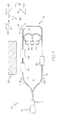
- FIG. 1 is a block an optical gyro 10 in accordance with a first exemplary embodiment of the present invention.
- one or more components of the optical gyro 10 are formed in or on a substrate 11 and interconnected with a silicon waveguide 16 formed in the substrate 11.
- the substrate 11 may be silicon, silicon-on-insulator (SOI), or the like, such as found in a microchip or other semiconductor related device, having one or more layers, such as an insulator layer of SiO 2 .
- SOI silicon-on-insulator
- the substrate 11 is described as an SOI substrate.
- the optical gyro 10 comprises a light source 12 (e.g., a monochromatic laser diode), an optical phase modulation network 30, 34, 36, a ring resonator 18, a detector array 32, 33, 35, and the silicon waveguide 16 (e.g., an SOI thin film waveguide) interconnecting the light source 12, the optical phase modulation network 30, 34, 36, the detector array 32, 33, 35, and the ring resonator 18.
- the optical gyro 10 further comprises a drive/detector circuit 38 that is coupled to the detector array 32, 33, 35 via metal interconnects (not shown) and provides the drive, control, and amplification functions of the detector array 32, 33, 35.
- the drive/detector circuit 38 may be a discrete device that is formed or mounted onto the substrate 11 or an integrated device that is formed in the substrate 11.
- the silicon waveguide 16 routes light beams between the components of the optical gyro 10.
- the waveguide 16 is formed by etching trenches in the silicon of the SOI substrate 11 and depositing SiO 2 in the trenches such that the silicon waveguide 16 is bordered by SiO 2 .
- the resulting silicon waveguide 16 confines the light beams in the silicon by index guiding (e.g., using the change in the refractive index for silicon and the refractive index for SiO 2 ).
- the silicon waveguide 16 is formed with a photonic crystal pattern in the silicon of the SOI substrate. The processes of etching layers and depositing materials applied in semiconductor fabrication techniques may be used to form the waveguide 16.
- the silicon waveguide 16 is formed on an SOI type substrate, other types of substrates and processes may be used to fabricate the silicon waveguide 16. Additionally, although the optical gyro 10 uses a silicon waveguide 16 to route the light beams from one component to another component, other materials (e.g., alumina, nitrides, III-V elements, other refractory materials, and the like) having optical properties similar to silicon and having similar refractive index contrasts (e.g., silicon and SiO 2 ) may be used for the waveguide. Although referred to as one waveguide, the silicon waveguide 16 may be a network of multiple interconnected waveguides.
- the light beams routed by the silicon waveguide 16 originate from the light source 12.
- a coupling element 14 e.g., a spot-size converter
- the light source 12 is preferably implemented to exhibit frequency stability, substantially narrow line width, substantially single frequency operation, and relatively high power capability and produces first and second light beams (e.g., a clockwise (CW) beam and a counter-clockwise (CCW) beam) that propagate through the waveguide 16 to the optical phase modulation network 30, 34, 36.
- first and second light beams e.g., a clockwise (CW) beam and a counter-clockwise (CCW) beam
- the light source 12 is a single frequency tunable laser that generates a light beam having a frequency f 0 , and this light beam is split (e.g., via a beam splitter (not shown) or by dividing the waveguide 16 into two portions 13 and 15) to form the first and second light beams (e.g., CW beam and CCW beam).
- the light source 12 includes first and second tunable lasers that synthesize the first and second light beams, respectively. The first light beam produced by the first laser is tuned to a frequency f 0 , and the second light beam produced by the second laser is tuned to a frequency f 0 + ⁇ f.
- the relative frequency drift and jitter between the two laser frequencies should be substantially minimized to a level that minimizes or does not affect the accuracy and stability of the frequency shift, and thus rotational rate, measurement.
- This can be accomplished by laser frequency stabilization techniques, such as those that use electronic servos to lock their beat frequencies to a tunable but stable offset (proportional to rotational rate).
- the optical phase modulation network 30, 34, 36 modulates the first and second light beams and comprises a first modulator 30 coupled to a first portion 13 of the waveguide 16, and second and third series-coupled modulators 34 and 36 coupled to a second portion 15 of the waveguide 16. Additional or fewer modulators may be used.
- the first modulator 30 receives and modulates the first light beam (e.g., CW beam) from the light source 12, and the second wave modulator 34 receives and modulates the second light beam (e.g., CCW beam) from the light source 12.
- the third modulator 36 receives the modulated light beam from the second modulator 34 and shifts the frequency of the modulated light beam.
- Each of the modulators 30, 34, 36 may be any one of a p-type insulator n-type (PIN) diode, metal-oxide semiconductor (MOS) capacitor (e.g., a silicon-insulator-silicon capacitor), or other devices that may implement a modulator and that may be integrated into the waveguide 16.
- MOS metal-oxide semiconductor
- Each of the modulators 30, 34, 36 is capable of modulating the electrical carrier concentration and refractive index in the waveguide 16 to modulate the phase of the light beams from the light source 12. These modulated light beams are introduced to the ring resonator 18.
- the ring resonator 18 comprises a set of reflective elements 20, 22, 24, 26 formed in the silicon of the SOI substrate 11, and the light beams introduced into the ring resonator 18 are circulated in counter-propagating directions (e.g., CW and CCW directions) via the reflective elements 20, 22, 24, 26 in a silicon region 28 (e.g., of the silicon layer in the SOI substrate 11) between the reflective elements 20, 22, 24, 26.
- the reflective elements 20, 22, 24, 26 are trenches etched in the silicon of the SOI substrate 11 and deposited with SiO 2 .
- a reflective surface 19, 21, 23, 25 is formed on each of the reflective elements 20, 22, 24, 26, respectively, by the refractive index contrast between silicon and SiO 2 .
- the reflective elements 20, 24, and 26 are photonic crystal hole structures etched in the silicon of the SOI substrate 11 and filled with SiO 2 that produce the reflective surfaces 19, 23. and 25, respectively.
- a first reflective element 22 introduces a portion of each of the modulated light beams into the ring resonator 18, and the reflective surfaces 19, 21, 23, 25 of the reflective elements 20, 22, 24, 26 are positioned to circulate these light beams (e.g., a first circulating light beam or CW circulating beam and a second circulating light beam or CCW circulating beam) in the ring resonator 18.
- the CW beam introduced by the reflective element 22 is directed to the reflective element 26, to the reflective element 24, to the reflective element 20, and back to the reflective element 22, thus propagating in the CW direction along a closed optical path in the silicon region 28.
- the CCW beam introduced by the reflective element 22 is directed to the reflective element 20, to the reflective element 24, to the reflective element 26, and to the reflective element 22 thus propagating in the CCW direction along the closed optical path in the silicon region 28.
- Additional reflective elements or a faceted cavity may be formed in the silicon of the SOI substrate 11 to increase the path length of the closed optical path.
- the frequency f 0 of the first light beam (e.g., CW beam) is tuned (e.g., by tuning the frequency of the light source 12) to the resonance frequency of the ring resonator 18 in the CW direction.
- the modulator 36 tunes the frequency ⁇ f to align the second light beam (e.g., CCW beam) frequency with a resonance center relative to the resonance frequency of the ring resonator 18 in the CCW direction.
- the modulator 36 shifts the frequency of the second light beam by an amount ⁇ f and directs the frequency shifted light to the ring resonator 18 to propagate in the CCW direction.
- the modulator 36 uses a serrodyne modulation waveform to accomplish frequency shifting.
- the CCW light beam from the light source 12 is phase modulated with a serrodyne signal whereby a phase ramp is applied to the input light beam (CCW beam).
- a frequency shift may be obtained, that is proportional to the slope of the phase ramp.
- a sawtooth waveform having a 2 ⁇ phase height and a frequency ⁇ f produces substantially equivalent results as the continuous ramp, and the sawtooth frequency ( ⁇ f) may be adjusted to track the CCW resonance in the presence of rotation.
- Another exemplary method for accomplishing a frequency shift is the use of an acousto-optic frequency shifter.
- the acoustic-optic frequency shifter may be an acousto-optic device formed or placed onto the substrate 11.
- the CW and CCW circulating light beams produce light outputs from the ring resonator 18 to the silicon waveguide 16 via reflective element 22.
- a resonance line shape may be detected by the detectors 32 and 35 in the detector array 32, 33, 35.
- a first detector 32 detects the resonance lineshape associated with the CCW circulating light beam
- a second detector 35 detects the resonance lineshape associated with the CW circulating light beam.
- Each of the detectors of the detector array 32, 33, 35 may be a germanium diode, or similar device, formed in the silicon waveguide 16 or a discrete device mounted on the silicon waveguide 16, and additional or fewer detectors may be used.
- the detectors monitor the incident and return signals (e.g., CW and CCW input light beams and the light outputs of the CW and CCW circulating light beams).
- the detector 33 measures the beat frequency between the input beams to the resonator 18, which is a measure of the resonance frequency shift due to the rotation rate.
- Each input light beam (e.g., CW beam and CCW beam) is sinusoidally phase-modulated in modulators 30 and 34, and therefore frequency modulated at frequencies f m and f n , respectively, to dither each input beam frequency across a resonance lineshape as measured by the detectors 35 and 32 in the detector array 32, 33, 35.
- the drive/detector circuit 38 coupled to the detector array 32, 33, 35 demodulates the output of the detectors 35 and 32 at frequencies f m and f n , respectively, to measure resonance centers indicated by the light outputs of the CW and CCW circulating light beams.
- the detectors 35 and 32 detect a minimum output at the fundamental frequencies f m and f n , respectively.
- an error signal at frequencies f m and f n , respectively, is sensed by the detectors 35 and 32 and used to tune the respective beam frequency to the respective resonance frequency of the ring resonator 18.
- the frequency of the CW beam is tuned by changing the frequency of the laser, f 0 , and the frequency of the CCW beam is adjusted via a feedback loop that changes the frequency shift, ⁇ f, of the modulator 36 so that f0 + ⁇ f matches the CCW resonance frequency of the resonator 18.
- the energy from the CCW beam does not produce a maximum intensity at the optical sensor 16.
- the CCW beam has a minimum output, i.e., a resonance dip, thereby indicating the resonance center.
- the energy of the CW beam enters the closed optical path of the ring resonator 18 when the CW beam is tuned to the resonance frequency of the ring resonator 18 in the CW direction.
- the round-trip path-lengths of the CW and CCW circulating light beams inside the ring resonator 18 in the CW and CCW direction, respectively, are substantially equal.
- ⁇ f is tuned to zero by the modulator 36.
- the round-trip path-lengths differ between the CW and the CCW directions producing a resonance frequency difference between the two directions that is proportional to the rotation rate.
- the rotation rate is determined.
- the optical gyro 10 senses a rotation rate about an axis (A) of the ring resonator 18.
- the drive/detector circuit 38 determines the rotation rate based on the resonance frequency difference between the two directions of the closed optical path of the ring resonator 18.
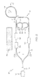
- FIG. 2 is a block diagram of an optical gyro 40 in accordance with a second exemplary embodiment of the present invention.
- the optical gyro 40 replaces the ring resonator 18, shown in FIG. 1, with a ring resonator 42.
- the ring resonator 42 comprises the reflective element 22 and a second silicon waveguide 44 coupled to the reflective element 22.
- the modulated light beams are introduced to the silicon waveguide 44 via the reflective element 22 to propagate in the CW and CCW directions, respectively.
- the silicon waveguide 44 may be formed in a similar manner and has similar optical properties as the silicon waveguide 16.
- the silicon waveguide 44 is formed by etching trenches in the silicon of the SOI substrate 11 and depositing SiO 2 in the trenches or arrays of holes such that the silicon waveguide 44 is bordered by SiO 2 -
- the silicon waveguide 44 is formed with a photonic crystal pattern in the silicon of the SOI substrate 11.
- the reflective element 22 may be replaced with an optical coupler fabricated from two coupled waveguides, each of which is made from the same structure as the resonator waveguide.
- the CW and CCW circulating light beams are directed by the silicon waveguide 44 in counter-propagating directions (e.g., CW and CCW directions, respectively) from one end of the silicon waveguide 44 to the other end and reflected by the reflective element 22.
- the path length of the silicon waveguide 44 may be modified (e.g., encircle the optical gyro 40) to encircle a greater effective area and thereby adjust the sensitivity of optical gyro 40 to rotation about the axis A, via the Sagnac effect.
- the axis of rotation A is perpendicular to the plane of the silicon waveguide 44.
- the silicon waveguide 44 is preferably a substantially circular shape, maximizine the area of the waveguide 44, and the axis A is perpendicular to the plane of the waveguide.
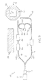
- FIG. 3 is a block diagram of an optical gyro 50 in accordance with a third exemplary embodiment of the present invention.
- the optical gyro 50 replaces the ring resonator 18, shown in FIG. 1, with a ring resonator 52.
- the ring resonator 52 comprises a trench 54, etched in the silicon of the SOI substrate 11, having a surface 56 that circulates portions of the input light beam (e.g., CW light beam or CCW light beam) in free space along a closed optical path around an axis A of the ring resonator 52.
- the input light beam e.g., CW light beam or CCW light beam
- the path of light beams enclosed by the surface 56 is free space, either vacuum, air, or other gas, such that the index of refraction experienced by the light in the trench is substantially unity as compared with a solid medium.
- the closed optical path encircles an effective area.
- the surface 56 may be mirrored to increase the reflective properties of the surface 56.
- the trench 54 may be enlarged to expand the surface 56 and increase the effective area, thereby increasing the sensitivity of the optical gyro 50 to rotation about the axis A via the Sagnac effect.
- the surface 56 may be constructed of multiple reflecting surfaces to direct the CW and CCW circulating light beams along one or more loops encircling the effective area to thereby increasing the signal to noise sensitivity of the optical gyro 50 to rotation about the axis A via the Sagnac effect.
- the path length of the closed optical path may be increased while substantially preserving the effective area encircled by the light beam.
- FIG. 4 is a flow diagram of a method 100 for sensing a rotation rate of a ring resonator in accordance with an exemplary embodiment of the present invention.
- the ring resonator is formed in a substrate having an insulator layer and a silicon layer.
- the first and second light beams are directed to the ring resonator via a first silicon waveguide formed in or on the insulator layer at step 105.
- a portion of the first light beam, or first circulating light beam, is circulated in a first counter-propagating direction (e.g., CW direction) of the ring resonator and a portion of the second light beam, or second circulating light beam, is circulated in a second counter-propagating direction (e.g., CCW direction) of the ring resonator at step 110.
- the first circulating light beam measures or is turned to a first resonance frequency associated with propagation in the CW direction of the ring resonator
- the second circulating light beam measures or is tuned to a second resonance frequency associated with propagation in the CCW direction.
- the first and second circulating light beams are directed along a closed optical path in a portion of the silicon layer.
- the ring resonator comprises a set of reflecting elements formed in the silicon layer, each of the set of reflecting elements comprising SiO 2 .
- the first and second circulating light beams are directed along a closed optical path in the silicon layer by these reflecting elements.
- the ring resonator comprises a set of reflecting elements each comprising a structure of photonic crystal holes formed in the silicon layer.
- the first and second circulating light beams are directed along a closed optical path in the silicon layer by these reflecting elements.
- the ring resonator comprises a trench formed in the silicon layer. The trench has a reflective surface, and the first and second circulating light beams are directed along a closed optical path in free space via the reflective surface of the trench.
- a frequency shift is measured between the first resonance frequency (e.g., of the first counter-propagating direction (CW direction) of the ring resonator) and the second resonance frequency (e.g., of the second counter-propagating direction (CCW direction) of the ring resonator at step 115.
- the frequency shift indicates the rotation rate.
- each of the disclosed optical gyros 10, 40, 50 include, but are not limited to: a capability of providing about a 1 deg/hr bias and about a 0.1 deg/root-hr angle random walk (ARW) in a low-cost, small-sized package; a resonator having a very low loss; use of a high reflectivity mirror rather than an optical coupler using waveguides to circulate light in the ring resonator; a compact, stable laser component that can be mounted on a silicon optical bench or an optical bench using a different substrate material; ease of coupling light from the source to the resonator; ease of interfacing to signal processing electronics in the same platform as the optics or ease of integration and electronics in the same platform; elimination of non-linear effects in silica fibers or other waveguide materials that may promote gyro errors; substantial reduction of light loss at transition point to resonator 14; a capability of circulating the light beams in very tight (e.g., pencil diameter or smaller) loops with
- the optical gyro 10, 40, 50 is constructed with an SOI electro-optical circuit that integrates electronics and optics and provides an efficient, expedient, self-aligned, and mechanically stable interface between the two.
- Optical functions such as associated with the coupling element 14 and the modulators 30, 34, and 36 may be formed in the thin silicon film of the SOI substrate. Since the optical and electrical characteristics of the silicon film are compatible, signal processing circuitry and optical sensing elements can also be integrated into the silicon layer, and miniature optical components having a feature size of as little as 10 microns may be mounted on silicon surfaces to eliminate large bulk optics, even when the light wave is needed to travel in free space instead of in a waveguide, such as in the resonator path itself.
- Laser diodes and external elements for stabilizing their frequency may also be mounted on the top surface of the substrate.
- the laser and any related frequency tuning components may be mounted on the substrate, and using the serrodyne method for frequency shifting enables the use of an integrated optical phase modulator in a silicon waveguide for the frequency shifter.
- Other ways of coupling light from free space optics to waveguides may be incorporated, such as the use of tapered or graded index structures that adiabatically couple light into the waveguide, or the use of gratings or prisms. The use of these techniques allows the fabrication of optics in a silicon platform and thus integrated with the electronics.
- the optical gyro 10, 40, 50 is suited to a variety of applications including, by way of example and not of limitation, applications requiring inertial guidance such as aircraft, land vehicle, submarine, satellite, surface ship navigation, and the like.
- applications requiring inertial guidance such as aircraft, land vehicle, submarine, satellite, surface ship navigation, and the like.
- the relatively small size envisioned for the optical gyro 10 would enable a practical usage on very small platforms including, by way of example and not of limitation, small robots, individual soldier footwear, and small-scale satellites.
Landscapes
- Physics & Mathematics (AREA)
- Engineering & Computer Science (AREA)
- Optics & Photonics (AREA)
- Electromagnetism (AREA)
- Power Engineering (AREA)
- General Physics & Mathematics (AREA)
- Radar, Positioning & Navigation (AREA)
- Remote Sensing (AREA)
- Gyroscopes (AREA)
Applications Claiming Priority (1)
| Application Number | Priority Date | Filing Date | Title |
|---|---|---|---|
| US11/433,965 US7535576B2 (en) | 2006-05-15 | 2006-05-15 | Integrated optical rotation sensor and method for sensing rotation rate |
Publications (2)
| Publication Number | Publication Date |
|---|---|
| EP1857779A1 true EP1857779A1 (fr) | 2007-11-21 |
| EP1857779B1 EP1857779B1 (fr) | 2017-07-05 |
Family
ID=38325345
Family Applications (1)
| Application Number | Title | Priority Date | Filing Date |
|---|---|---|---|
| EP07108242.4A Ceased EP1857779B1 (fr) | 2006-05-15 | 2007-05-15 | Capteur optique intégré de vitesse de rotation et méthode de mesure de vitesse de rotation |
Country Status (3)
| Country | Link |
|---|---|
| US (1) | US7535576B2 (fr) |
| EP (1) | EP1857779B1 (fr) |
| JP (1) | JP5474282B2 (fr) |
Cited By (1)
| Publication number | Priority date | Publication date | Assignee | Title |
|---|---|---|---|---|
| WO2014042049A1 (fr) * | 2012-09-14 | 2014-03-20 | 株式会社ブイ・テクノロジー | Appareil laser en anneau à semi-conducteur |
Families Citing this family (14)
| Publication number | Priority date | Publication date | Assignee | Title |
|---|---|---|---|---|
| US7924427B2 (en) * | 2006-09-27 | 2011-04-12 | Northrop Grumman Guidance & Electronics Company | Photonic crystal based rotation sensor |
| US7668420B2 (en) * | 2007-07-26 | 2010-02-23 | Hewlett-Packard Development Company, L.P. | Optical waveguide ring resonator with an intracavity active element |
| US8009296B2 (en) * | 2009-12-13 | 2011-08-30 | Honeywell International Inc. | Light-phase-noise error reducer |
| US7933020B1 (en) | 2009-12-13 | 2011-04-26 | Honeywell International Inc. | System and method for reducing laser phase noise in a resonator fiber optic gyroscope |
| CN102003959B (zh) * | 2010-10-09 | 2012-05-23 | 浙江大学 | 一种环形光学微腔式光纤陀螺 |
| US8736845B2 (en) * | 2011-05-24 | 2014-05-27 | Honeywell International Inc. | Frequency stabilized laser system |
| KR101682993B1 (ko) | 2011-12-23 | 2016-12-20 | 인텔 코포레이션 | 집적 실리콘 광기계 자이로스코프 |
| US20150022818A1 (en) * | 2012-06-08 | 2015-01-22 | The Board Of Trustees Of The Leland Stanford Junior University | Laser-driven optical gyroscope with push-pull modulation |
| US8923352B2 (en) | 2012-08-10 | 2014-12-30 | Honeywell International Inc. | Laser with transmission and reflection mode feedback control |
| US10228250B2 (en) | 2016-09-20 | 2019-03-12 | The Board Of Trustees Of The Leland Stanford Junior University | Optical system and method utilizing a laser-driven light source with white noise modulation |
| US9923335B1 (en) * | 2016-09-22 | 2018-03-20 | Oracle International Corporation | Thermally compensating spot-size converter for an athermal laser |
| US11624615B2 (en) * | 2020-10-05 | 2023-04-11 | Anello Photonics, Inc. | Ring waveguide based integrated photonics optical gyroscope with balanced detection scheme |
| US11231278B1 (en) | 2020-10-15 | 2022-01-25 | The Board Of Trustees Of The Leland Stanford Junior University | System and method for generating broadband spectrum by phase modulation of multiple wavelengths |
| TWI765412B (zh) * | 2020-11-13 | 2022-05-21 | 國立中山大學 | 矽光子積體電路及光纖陀螺儀裝置 |
Citations (5)
| Publication number | Priority date | Publication date | Assignee | Title |
|---|---|---|---|---|
| US4326803A (en) * | 1979-09-20 | 1982-04-27 | Northrop Corporation | Thin film laser gyro |
| US5163118A (en) * | 1986-11-10 | 1992-11-10 | The United States Of America As Represented By The Secretary Of The Air Force | Lattice mismatched hetrostructure optical waveguide |
| US5319727A (en) * | 1992-12-28 | 1994-06-07 | Honeywell Inc. | Ion-beam deposited, gain enhanced ring resonators |
| US6163632A (en) * | 1997-09-23 | 2000-12-19 | Bookham Technology Plc | Integrated optical circuit |
| US20040151463A1 (en) * | 2003-02-03 | 2004-08-05 | Motorola, Inc. | Optical waveguide structure and method for fabricating the same |
Family Cites Families (125)
| Publication number | Priority date | Publication date | Assignee | Title |
|---|---|---|---|---|
| US4234357A (en) * | 1979-07-16 | 1980-11-18 | Trw Inc. | Process for manufacturing emitters by diffusion from polysilicon |
| US4315693A (en) * | 1979-12-31 | 1982-02-16 | Walker Clifford G | Optical strapdown inertia system |
| US4673293A (en) * | 1985-01-31 | 1987-06-16 | Honeywell Inc. | Passive cavity gyro bias eliminator |
| US4886345A (en) * | 1988-08-05 | 1989-12-12 | Harris Corporation | Electro-optical phase modulator |
| GB2221999B (en) * | 1988-08-16 | 1992-09-16 | Plessey Co Plc | Optical phase modulator |
| US4958898A (en) * | 1989-03-15 | 1990-09-25 | The United States Of America As Represented By The Secretary Of The Air Force | Silicon double-injection electro-optic modulator with insulated-gate and method of using same |
| EP0393987A3 (fr) * | 1989-04-19 | 1992-08-05 | British Aerospace Public Limited Company | Gyroscope optique à résonateur en anneau |
| JPH04357408A (ja) * | 1991-01-25 | 1992-12-10 | Tokimec Inc | 光ジャイロの光学系の構造 |
| US5143577A (en) * | 1991-02-08 | 1992-09-01 | Hoechst Celanese Corporation | Smooth-wall polymeric channel and rib waveguides exhibiting low optical loss |
| JP2511346B2 (ja) * | 1991-11-12 | 1996-06-26 | 日本航空電子工業株式会社 | リング共振型ジャイロ |
| KR0134763B1 (ko) * | 1992-04-21 | 1998-04-23 | 다니이 아끼오 | 광도파로소자와 그 제조방법 |
| JPH06180233A (ja) * | 1992-12-11 | 1994-06-28 | Alps Electric Co Ltd | 光ジャイロ装置 |
| US5383048A (en) | 1993-02-03 | 1995-01-17 | Seaver; George | Stress-optical phase modulator and modulation system and method of use |
| JP2791412B2 (ja) * | 1993-03-18 | 1998-08-27 | 日本航空電子工業株式会社 | 光共振角速度計 |
| KR960011653B1 (ko) * | 1993-04-16 | 1996-08-24 | 현대전자산업 주식회사 | 디램 셀 및 그 제조방법 |
| JP2766974B2 (ja) * | 1993-06-18 | 1998-06-18 | 日本航空電子工業株式会社 | 受動型リング共振光ジャイロ |
| JP3377794B2 (ja) * | 1993-09-21 | 2003-02-17 | ブッカム・テクノロジイ・ピイエルシイ | 電気光学デバイス |
| US5429981A (en) * | 1994-06-30 | 1995-07-04 | Honeywell Inc. | Method of making linear capacitors for high temperature applications |
| US5696662A (en) * | 1995-08-21 | 1997-12-09 | Honeywell Inc. | Electrostatically operated micromechanical capacitor |
| JP2817703B2 (ja) * | 1996-04-25 | 1998-10-30 | 日本電気株式会社 | 光半導体装置 |
| US5841931A (en) * | 1996-11-26 | 1998-11-24 | Massachusetts Institute Of Technology | Methods of forming polycrystalline semiconductor waveguides for optoelectronic integrated circuits, and devices formed thereby |
| US5861651A (en) * | 1997-02-28 | 1999-01-19 | Lucent Technologies Inc. | Field effect devices and capacitors with improved thin film dielectrics and method for making same |
| US6147362A (en) * | 1997-03-17 | 2000-11-14 | Honeywell International Inc. | High performance display pixel for electronics displays |
| US5917967A (en) * | 1997-05-21 | 1999-06-29 | The United States Of America As Represented By The Secretary Of The Army | Techniques for forming optical electronic integrated circuits having interconnects in the form of semiconductor waveguides |
| US6418999B1 (en) * | 1997-12-26 | 2002-07-16 | Cannon Kabushiki Kaisha | Sample separating apparatus and method, and substrate manufacturing method |
| US6259089B1 (en) * | 1998-05-15 | 2001-07-10 | Rice Systems, Inc. | Integrated optics rotation sensor |
| US6108212A (en) * | 1998-06-05 | 2000-08-22 | Motorola, Inc. | Surface-mount device package having an integral passive component |
| US6381380B1 (en) * | 1998-06-24 | 2002-04-30 | The Trustees Of Princeton University | Twin waveguide based design for photonic integrated circuits |
| US6270604B1 (en) * | 1998-07-23 | 2001-08-07 | Molecular Optoelectronics Corporation | Method for fabricating an optical waveguide |
| JP2000124092A (ja) * | 1998-10-16 | 2000-04-28 | Shin Etsu Handotai Co Ltd | 水素イオン注入剥離法によってsoiウエーハを製造する方法およびこの方法で製造されたsoiウエーハ |
| US6493089B2 (en) * | 1998-10-19 | 2002-12-10 | Canon Kabushiki Kaisha | Gyro and method of operating the same with a modulated frequency signal |
| GB2343293B (en) * | 1998-10-23 | 2003-05-14 | Bookham Technology Ltd | Manufacture of a silicon waveguide structure |
| JP4416055B2 (ja) * | 1998-12-01 | 2010-02-17 | ローム株式会社 | 強誘電体メモリおよびその製造方法 |
| US6323985B1 (en) * | 1998-12-30 | 2001-11-27 | Intel Corporation | Mosfet through silicon modulator and method |
| US6150266A (en) * | 1999-01-28 | 2000-11-21 | Vlsi Technology, Inc. | Local interconnect formed using silicon spacer |
| US6690884B1 (en) * | 1999-02-19 | 2004-02-10 | Corvis Corporation | Optical transmission systems including error correction and protection apparatuses and methods |
| US6627954B1 (en) * | 1999-03-19 | 2003-09-30 | Silicon Wave, Inc. | Integrated circuit capacitor in a silicon-on-insulator integrated circuit |
| JP2001111160A (ja) * | 1999-04-19 | 2001-04-20 | Canon Inc | 半導体素子の製造方法及び半導体素子、リング共振器型半導体レーザ、ジャイロ |
| US6555288B1 (en) | 1999-06-21 | 2003-04-29 | Corning Incorporated | Optical devices made from radiation curable fluorinated compositions |
| JP2001042150A (ja) | 1999-07-30 | 2001-02-16 | Canon Inc | 光導波路、その作製方法、およびこれを用いた光インタコネクション装置 |
| SE0000148D0 (sv) | 2000-01-17 | 2000-01-17 | Forskarpatent I Syd Ab | Tillverkningsförfarande för IR-detektormatriser |
| US6546538B1 (en) * | 2000-03-10 | 2003-04-08 | Lsi Logic Corporation | Integrated circuit having on-chip capacitors for supplying power to portions of the circuit requiring high-transient peak power |
| FR2810991B1 (fr) * | 2000-06-28 | 2004-07-09 | Inst Francais Du Petrole | Procede pour l'hydrogenation de coupes contenant des hydrocarbures et notamment des molecules insaturees contenant au moins deux doubles liaisons ou au moins une triple liaison |
| JP4961634B2 (ja) | 2000-07-07 | 2012-06-27 | Kddi株式会社 | 光ゲート装置 |
| US6850683B2 (en) | 2000-07-10 | 2005-02-01 | Massachusetts Institute Of Technology | Low-loss waveguide and method of making same |
| US6561463B1 (en) | 2000-07-14 | 2003-05-13 | Honeywell International Inc. | Flight control module with integrated spoiler actuator control electronics |
| JP4558158B2 (ja) * | 2000-08-10 | 2010-10-06 | 東京航空計器株式会社 | 共振形光ファイバジャイロにおける偏波変動誘起ドリフトを低減させる方法および該方法を用いた装置 |
| DE60137447D1 (de) * | 2000-11-28 | 2009-03-05 | Rosemount Inc | Einrichtung zur messung physikalischer grössen mit einem optischen sensor |
| US7330271B2 (en) * | 2000-11-28 | 2008-02-12 | Rosemount, Inc. | Electromagnetic resonant sensor with dielectric body and variable gap cavity |
| US6674108B2 (en) | 2000-12-20 | 2004-01-06 | Honeywell International Inc. | Gate length control for semiconductor chip design |
| FR2819893B1 (fr) | 2001-01-25 | 2003-10-17 | Opsitech Optical System Chip | Structure optique integree a birefringence reduite |
| US6890450B2 (en) | 2001-02-02 | 2005-05-10 | Intel Corporation | Method of providing optical quality silicon surface |
| US6603166B2 (en) * | 2001-03-14 | 2003-08-05 | Honeywell International Inc. | Frontside contact on silicon-on-insulator substrate |
| US6633716B2 (en) | 2001-05-02 | 2003-10-14 | Motorola, Inc. | Optical device and method therefor |
| US6842546B2 (en) | 2001-05-17 | 2005-01-11 | Sioptical, Inc. | Polyloaded optical waveguide device in combination with optical coupler, and method for making same |
| US6963118B2 (en) | 2001-05-17 | 2005-11-08 | Sioptical, Inc. | Hybrid active and electronic circuit with evanescent coupling |
| US6690844B2 (en) | 2001-05-17 | 2004-02-10 | Optronx, Inc. | Optical fiber apparatus and associated method |
| US6898352B2 (en) | 2001-05-17 | 2005-05-24 | Sioptical, Inc. | Optical waveguide circuit including passive optical waveguide device combined with active optical waveguide device, and method for making same |
| US6690863B2 (en) * | 2001-05-17 | 2004-02-10 | Si Optical, Inc. | Waveguide coupler and method for making same |
| US6608945B2 (en) * | 2001-05-17 | 2003-08-19 | Optronx, Inc. | Self-aligning modulator method and associated apparatus |
| US6891685B2 (en) | 2001-05-17 | 2005-05-10 | Sioptical, Inc. | Anisotropic etching of optical components |
| US6625348B2 (en) * | 2001-05-17 | 2003-09-23 | Optron X, Inc. | Programmable delay generator apparatus and associated method |
| US6891985B2 (en) | 2001-05-17 | 2005-05-10 | Sioptical, Inc. | Polyloaded optical waveguide devices and methods for making same |
| US6738546B2 (en) * | 2001-05-17 | 2004-05-18 | Sioptical, Inc. | Optical waveguide circuit including multiple passive optical waveguide devices, and method of making same |
| US6646747B2 (en) * | 2001-05-17 | 2003-11-11 | Sioptical, Inc. | Interferometer apparatus and associated method |
| US6654511B2 (en) * | 2001-05-17 | 2003-11-25 | Sioptical, Inc. | Optical modulator apparatus and associated method |
| US6658173B2 (en) * | 2001-05-17 | 2003-12-02 | Optronx, Inc. | Interferometer and method of making same |
| US6493502B1 (en) * | 2001-05-17 | 2002-12-10 | Optronx, Inc. | Dynamic gain equalizer method and associated apparatus |
| US6947615B2 (en) | 2001-05-17 | 2005-09-20 | Sioptical, Inc. | Optical lens apparatus and associated method |
| US6526187B1 (en) * | 2001-05-17 | 2003-02-25 | Optronx, Inc. | Polarization control apparatus and associated method |
| US6748125B2 (en) * | 2001-05-17 | 2004-06-08 | Sioptical, Inc. | Electronic semiconductor control of light in optical waveguide |
| US6760498B2 (en) * | 2001-05-17 | 2004-07-06 | Sioptical, Inc. | Arrayed waveguide grating, and method of making same |
| US6912330B2 (en) | 2001-05-17 | 2005-06-28 | Sioptical Inc. | Integrated optical/electronic circuits and associated methods of simultaneous generation thereof |
| US6603889B2 (en) * | 2001-05-17 | 2003-08-05 | Optronx, Inc. | Optical deflector apparatus and associated method |
| US6596570B2 (en) | 2001-06-06 | 2003-07-22 | International Business Machines Corporation | SOI device with reduced junction capacitance |
| US20030026571A1 (en) | 2001-07-31 | 2003-02-06 | Michael Bazylenko | Method of reducing sidewall roughness of a waveguide |
| US6990257B2 (en) | 2001-09-10 | 2006-01-24 | California Institute Of Technology | Electronically biased strip loaded waveguide |
| US6816636B2 (en) * | 2001-09-12 | 2004-11-09 | Honeywell International Inc. | Tunable optical filter |
| JP3755588B2 (ja) | 2001-10-03 | 2006-03-15 | 日本電気株式会社 | 光制御デバイス |
| US6580863B2 (en) | 2001-10-31 | 2003-06-17 | Intel Corporation | System and method for providing integrated optical waveguide device |
| US20030098289A1 (en) | 2001-11-29 | 2003-05-29 | Dawei Zheng | Forming an optical mode transformer |
| WO2003065413A2 (fr) | 2002-01-30 | 2003-08-07 | Optronx, Inc. | Procede et appareil de modification de l'indice de mode effectif des guides d'ondes |
| JP2003234410A (ja) | 2002-02-08 | 2003-08-22 | Fujitsu Ltd | キャパシタ及びその製造方法並びに半導体装置 |
| JP3955764B2 (ja) | 2002-02-08 | 2007-08-08 | 富士通株式会社 | 電気光学効果により光位相を変化させる素子を搭載した光変調器 |
| IL148716A0 (en) | 2002-03-14 | 2002-09-12 | Yissum Res Dev Co | Control of optical signals by mos (cosmos) device |
| US6956983B2 (en) | 2002-05-31 | 2005-10-18 | Intel Corporation | Epitaxial growth for waveguide tapering |
| JP4154178B2 (ja) | 2002-06-21 | 2008-09-24 | キヤノン株式会社 | ビデオカメラ |
| US7010208B1 (en) | 2002-06-24 | 2006-03-07 | Luxtera, Inc. | CMOS process silicon waveguides |
| US6743662B2 (en) | 2002-07-01 | 2004-06-01 | Honeywell International, Inc. | Silicon-on-insulator wafer for RF integrated circuit |
| US6919238B2 (en) | 2002-07-29 | 2005-07-19 | Intel Corporation | Silicon on insulator (SOI) transistor and methods of fabrication |
| US6888219B2 (en) | 2002-08-29 | 2005-05-03 | Honeywell International, Inc. | Integrated structure with microwave components |
| US6845198B2 (en) | 2003-03-25 | 2005-01-18 | Sioptical, Inc. | High-speed silicon-based electro-optic modulator |
| US7118682B2 (en) | 2003-03-28 | 2006-10-10 | Sioptical, Inc. | Low loss SOI/CMOS compatible silicon waveguide and method of making the same |
| US6993225B2 (en) | 2004-02-10 | 2006-01-31 | Sioptical, Inc. | Tapered structure for providing coupling between external optical device and planar optical waveguide and method of forming the same |
| US6897498B2 (en) | 2003-03-31 | 2005-05-24 | Sioptical, Inc. | Polycrystalline germanium-based waveguide detector integrated on a thin silicon-on-insulator (SOI) platform |
| US7020364B2 (en) | 2003-03-31 | 2006-03-28 | Sioptical Inc. | Permanent light coupling arrangement and method for use with thin silicon optical waveguides |
| US6934444B2 (en) | 2003-04-10 | 2005-08-23 | Sioptical, Inc. | Beam shaping and practical methods of reducing loss associated with mating external sources and optics to thin silicon waveguides |
| US7000207B2 (en) | 2003-04-10 | 2006-02-14 | Sioptical, Inc. | Method of using a Manhattan layout to realize non-Manhattan shaped optical structures |
| US6980720B2 (en) | 2003-04-11 | 2005-12-27 | Sioptical, Inc. | Mode transformation and loss reduction in silicon waveguide structures utilizing tapered transition regions |
| US6968110B2 (en) | 2003-04-21 | 2005-11-22 | Sioptical, Inc. | CMOS-compatible integration of silicon-based optical devices with electronic devices |
| WO2004095084A2 (fr) | 2003-04-23 | 2004-11-04 | Siophcal, Inc. | Dispositifs a ondes lumineuses plans et submicroniques formes sur une plate-forme optique soi (silicium sur isolant) |
| EP1620755A4 (fr) | 2003-04-28 | 2006-05-24 | Sioptical Inc | Montage permettant de reduire la sensibilite aux longueurs d'onde dans des systemes optiques a base de silicium sur isolant couples avec un prisme |
| CA2523298C (fr) | 2003-05-08 | 2013-10-01 | Sioptical, Inc. | Modulateur electro-optique tres rapide a base de silicium |
| WO2005024470A2 (fr) | 2003-09-04 | 2005-03-17 | Sioptical, Inc | Structures de reseau externes d'interfaçage de sources optiques a multiplexage par repartition en longueur d'onde avec des guides d'ondes optiques minces |
| US7058261B2 (en) | 2003-09-04 | 2006-06-06 | Sioptical, Inc. | Interfacing multiple wavelength sources to thin optical waveguides utilizing evanescent coupling |
| DE602004027305D1 (de) | 2003-11-20 | 2010-07-01 | Sioptical Inc | Auf silizium basierender optischer schottky-barrieren-infrarotdetektor |
| US7113676B2 (en) | 2003-12-04 | 2006-09-26 | David Piede | Planar waveguide optical isolator in thin silicon-on-isolator (SOI) structure |
| US20050135727A1 (en) | 2003-12-18 | 2005-06-23 | Sioptical, Inc. | EMI-EMC shield for silicon-based optical transceiver |
| US7672558B2 (en) | 2004-01-12 | 2010-03-02 | Honeywell International, Inc. | Silicon optical device |
| US7013067B2 (en) | 2004-02-11 | 2006-03-14 | Sioptical, Inc. | Silicon nanotaper couplers and mode-matching devices |
| US7298949B2 (en) | 2004-02-12 | 2007-11-20 | Sioptical, Inc. | SOI-based photonic bandgap devices |
| US7106448B1 (en) * | 2004-02-17 | 2006-09-12 | Sandia Corporation | Integrated resonant micro-optical gyroscope and method of fabrication |
| CA2557509C (fr) | 2004-02-26 | 2014-09-30 | Sioptical, Inc. | Manipulation active de la lumiere dans une structure de silicium sur isolant (soi) |
| WO2005086786A2 (fr) | 2004-03-08 | 2005-09-22 | Sioptical, Inc. | Dispositif et procede permettant de realiser des essais opto-electroniques au niveau des tranches |
| US7217584B2 (en) | 2004-03-18 | 2007-05-15 | Honeywell International Inc. | Bonded thin-film structures for optical modulators and methods of manufacture |
| US7177489B2 (en) | 2004-03-18 | 2007-02-13 | Honeywell International, Inc. | Silicon-insulator-silicon thin-film structures for optical modulators and methods of manufacture |
| US7149388B2 (en) | 2004-03-18 | 2006-12-12 | Honeywell International, Inc. | Low loss contact structures for silicon based optical modulators and methods of manufacture |
| CA2560845C (fr) | 2004-03-24 | 2011-05-24 | Sioptical, Inc. | Recouvrement optique en silicium mince |
| US20050214989A1 (en) | 2004-03-29 | 2005-09-29 | Honeywell International Inc. | Silicon optoelectronic device |
| US20050236619A1 (en) | 2004-04-21 | 2005-10-27 | Vipulkumar Patel | CMOS-compatible integration of silicon-based optical devices with electronic devices |
| US7269809B2 (en) | 2004-06-23 | 2007-09-11 | Sioptical, Inc. | Integrated approach for design, simulation and verification of monolithic, silicon-based opto-electronic circuits |
| US20060018597A1 (en) | 2004-07-23 | 2006-01-26 | Sioptical, Inc. | Liquid crystal grating coupling |
| US20060038144A1 (en) | 2004-08-23 | 2006-02-23 | Maddison John R | Method and apparatus for providing optimal images of a microscope specimen |
| US20060063679A1 (en) | 2004-09-17 | 2006-03-23 | Honeywell International Inc. | Semiconductor-insulator-semiconductor structure for high speed applications |
| JP2008517332A (ja) * | 2004-10-19 | 2008-05-22 | シオプティカル インコーポレーテッド | モノリシック集積した光学及び電子構造におけるフィードバック制御としての光検出器構造及び使用 |
-
2006
- 2006-05-15 US US11/433,965 patent/US7535576B2/en active Active
-
2007
- 2007-05-15 EP EP07108242.4A patent/EP1857779B1/fr not_active Ceased
- 2007-05-15 JP JP2007129255A patent/JP5474282B2/ja not_active Expired - Fee Related
Patent Citations (5)
| Publication number | Priority date | Publication date | Assignee | Title |
|---|---|---|---|---|
| US4326803A (en) * | 1979-09-20 | 1982-04-27 | Northrop Corporation | Thin film laser gyro |
| US5163118A (en) * | 1986-11-10 | 1992-11-10 | The United States Of America As Represented By The Secretary Of The Air Force | Lattice mismatched hetrostructure optical waveguide |
| US5319727A (en) * | 1992-12-28 | 1994-06-07 | Honeywell Inc. | Ion-beam deposited, gain enhanced ring resonators |
| US6163632A (en) * | 1997-09-23 | 2000-12-19 | Bookham Technology Plc | Integrated optical circuit |
| US20040151463A1 (en) * | 2003-02-03 | 2004-08-05 | Motorola, Inc. | Optical waveguide structure and method for fabricating the same |
Cited By (1)
| Publication number | Priority date | Publication date | Assignee | Title |
|---|---|---|---|---|
| WO2014042049A1 (fr) * | 2012-09-14 | 2014-03-20 | 株式会社ブイ・テクノロジー | Appareil laser en anneau à semi-conducteur |
Also Published As
| Publication number | Publication date |
|---|---|
| JP2007309937A (ja) | 2007-11-29 |
| US7535576B2 (en) | 2009-05-19 |
| EP1857779B1 (fr) | 2017-07-05 |
| US20070263224A1 (en) | 2007-11-15 |
| JP5474282B2 (ja) | 2014-04-16 |
Similar Documents
| Publication | Publication Date | Title |
|---|---|---|
| EP1857779B1 (fr) | Capteur optique intégré de vitesse de rotation et méthode de mesure de vitesse de rotation | |
| JP4818979B2 (ja) | 外部共振器ビーム発生器を備える光共振器ジャイロ | |
| EP2495529B1 (fr) | Gyroscope résonateur optique | |
| US7751055B2 (en) | Hollow core fiber optical gyro | |
| US10921125B2 (en) | Optical gyroscope | |
| US7362443B2 (en) | Optical gyro with free space resonator and method for sensing inertial rotation rate | |
| JP5784653B2 (ja) | 伝送モードrfogおよびrfogで回転を検出する方法 | |
| US7372574B2 (en) | System and method for stabilizing light sources in resonator gyro | |
| EP2128566B1 (fr) | Résonateur fiable à fibres creuses à faible perte | |
| Sanders et al. | Development of compact resonator fiber optic gyroscopes | |
| EP1946043B1 (fr) | Cavite de polarisation pour rfog et procede de detection de la vitesse de rotation d'un resonateur |
Legal Events
| Date | Code | Title | Description |
|---|---|---|---|
| PUAI | Public reference made under article 153(3) epc to a published international application that has entered the european phase |
Free format text: ORIGINAL CODE: 0009012 |
|
| AK | Designated contracting states |
Kind code of ref document: A1 Designated state(s): AT BE BG CH CY CZ DE DK EE ES FI FR GB GR HU IE IS IT LI LT LU LV MC MT NL PL PT RO SE SI SK TR |
|
| AX | Request for extension of the european patent |
Extension state: AL BA HR MK YU |
|
| 17P | Request for examination filed |
Effective date: 20080508 |
|
| 17Q | First examination report despatched |
Effective date: 20080611 |
|
| AKX | Designation fees paid |
Designated state(s): DE FR |
|
| RAP1 | Party data changed (applicant data changed or rights of an application transferred) |
Owner name: HONEYWELL INTERNATIONAL INC. |
|
| GRAP | Despatch of communication of intention to grant a patent |
Free format text: ORIGINAL CODE: EPIDOSNIGR1 |
|
| INTG | Intention to grant announced |
Effective date: 20170217 |
|
| RIC1 | Information provided on ipc code assigned before grant |
Ipc: G01C 19/72 20060101AFI20170206BHEP |
|
| GRAS | Grant fee paid |
Free format text: ORIGINAL CODE: EPIDOSNIGR3 |
|
| GRAA | (expected) grant |
Free format text: ORIGINAL CODE: 0009210 |
|
| AK | Designated contracting states |
Kind code of ref document: B1 Designated state(s): DE FR |
|
| REG | Reference to a national code |
Ref country code: DE Ref legal event code: R096 Ref document number: 602007051529 Country of ref document: DE |
|
| REG | Reference to a national code |
Ref country code: DE Ref legal event code: R097 Ref document number: 602007051529 Country of ref document: DE |
|
| PLBE | No opposition filed within time limit |
Free format text: ORIGINAL CODE: 0009261 |
|
| STAA | Information on the status of an ep patent application or granted ep patent |
Free format text: STATUS: NO OPPOSITION FILED WITHIN TIME LIMIT |
|
| REG | Reference to a national code |
Ref country code: FR Ref legal event code: PLFP Year of fee payment: 12 |
|
| 26N | No opposition filed |
Effective date: 20180406 |
|
| PGFP | Annual fee paid to national office [announced via postgrant information from national office to epo] |
Ref country code: FR Payment date: 20200527 Year of fee payment: 14 Ref country code: DE Payment date: 20200529 Year of fee payment: 14 |
|
| REG | Reference to a national code |
Ref country code: DE Ref legal event code: R119 Ref document number: 602007051529 Country of ref document: DE |
|
| PG25 | Lapsed in a contracting state [announced via postgrant information from national office to epo] |
Ref country code: DE Free format text: LAPSE BECAUSE OF NON-PAYMENT OF DUE FEES Effective date: 20211201 |
|
| PG25 | Lapsed in a contracting state [announced via postgrant information from national office to epo] |
Ref country code: FR Free format text: LAPSE BECAUSE OF NON-PAYMENT OF DUE FEES Effective date: 20210531 |
|
| P01 | Opt-out of the competence of the unified patent court (upc) registered |
Effective date: 20230525 |