EP1857790A2 - Source d'illumination dotée d'un matériau photoluminescent et d'un filtre, et appareil l'incluant - Google Patents
Source d'illumination dotée d'un matériau photoluminescent et d'un filtre, et appareil l'incluant Download PDFInfo
- Publication number
- EP1857790A2 EP1857790A2 EP07100618A EP07100618A EP1857790A2 EP 1857790 A2 EP1857790 A2 EP 1857790A2 EP 07100618 A EP07100618 A EP 07100618A EP 07100618 A EP07100618 A EP 07100618A EP 1857790 A2 EP1857790 A2 EP 1857790A2
- Authority
- EP
- European Patent Office
- Prior art keywords
- photoluminescent material
- material layer
- illumination source
- emitting device
- light emitting
- Prior art date
- Legal status (The legal status is an assumption and is not a legal conclusion. Google has not performed a legal analysis and makes no representation as to the accuracy of the status listed.)
- Withdrawn
Links
Images


Classifications
-
- G—PHYSICS
- G01—MEASURING; TESTING
- G01J—MEASUREMENT OF INTENSITY, VELOCITY, SPECTRAL CONTENT, POLARISATION, PHASE OR PULSE CHARACTERISTICS OF INFRARED, VISIBLE OR ULTRAVIOLET LIGHT; COLORIMETRY; RADIATION PYROMETRY
- G01J3/00—Spectrometry; Spectrophotometry; Monochromators; Measuring colours
- G01J3/02—Details
- G01J3/10—Arrangements of light sources specially adapted for spectrometry or colorimetry
-
- G—PHYSICS
- G01—MEASURING; TESTING
- G01J—MEASUREMENT OF INTENSITY, VELOCITY, SPECTRAL CONTENT, POLARISATION, PHASE OR PULSE CHARACTERISTICS OF INFRARED, VISIBLE OR ULTRAVIOLET LIGHT; COLORIMETRY; RADIATION PYROMETRY
- G01J1/00—Photometry, e.g. photographic exposure meter
- G01J1/58—Photometry, e.g. photographic exposure meter using luminescence generated by light
-
- G—PHYSICS
- G01—MEASURING; TESTING
- G01N—INVESTIGATING OR ANALYSING MATERIALS BY DETERMINING THEIR CHEMICAL OR PHYSICAL PROPERTIES
- G01N21/00—Investigating or analysing materials by the use of optical means, i.e. using sub-millimetre waves, infrared, visible or ultraviolet light
- G01N21/17—Systems in which incident light is modified in accordance with the properties of the material investigated
- G01N21/25—Colour; Spectral properties, i.e. comparison of effect of material on the light at two or more different wavelengths or wavelength bands
- G01N21/27—Colour; Spectral properties, i.e. comparison of effect of material on the light at two or more different wavelengths or wavelength bands using photo-electric detection ; circuits for computing concentration
- G01N21/274—Calibration, base line adjustment, drift correction
- G01N21/278—Constitution of standards
-
- G—PHYSICS
- G01—MEASURING; TESTING
- G01N—INVESTIGATING OR ANALYSING MATERIALS BY DETERMINING THEIR CHEMICAL OR PHYSICAL PROPERTIES
- G01N21/00—Investigating or analysing materials by the use of optical means, i.e. using sub-millimetre waves, infrared, visible or ultraviolet light
- G01N21/17—Systems in which incident light is modified in accordance with the properties of the material investigated
- G01N21/25—Colour; Spectral properties, i.e. comparison of effect of material on the light at two or more different wavelengths or wavelength bands
- G01N21/31—Investigating relative effect of material at wavelengths characteristic of specific elements or molecules, e.g. atomic absorption spectrometry
-
- H—ELECTRICITY
- H10—SEMICONDUCTOR DEVICES; ELECTRIC SOLID-STATE DEVICES NOT OTHERWISE PROVIDED FOR
- H10H—INORGANIC LIGHT-EMITTING SEMICONDUCTOR DEVICES HAVING POTENTIAL BARRIERS
- H10H20/00—Individual inorganic light-emitting semiconductor devices having potential barriers, e.g. light-emitting diodes [LED]
- H10H20/80—Constructional details
- H10H20/84—Coatings, e.g. passivation layers or antireflective coatings
-
- H—ELECTRICITY
- H10—SEMICONDUCTOR DEVICES; ELECTRIC SOLID-STATE DEVICES NOT OTHERWISE PROVIDED FOR
- H10H—INORGANIC LIGHT-EMITTING SEMICONDUCTOR DEVICES HAVING POTENTIAL BARRIERS
- H10H20/00—Individual inorganic light-emitting semiconductor devices having potential barriers, e.g. light-emitting diodes [LED]
- H10H20/80—Constructional details
- H10H20/85—Packages
- H10H20/851—Wavelength conversion means
- H10H20/8515—Wavelength conversion means not being in contact with the bodies
-
- H—ELECTRICITY
- H10—SEMICONDUCTOR DEVICES; ELECTRIC SOLID-STATE DEVICES NOT OTHERWISE PROVIDED FOR
- H10W—GENERIC PACKAGES, INTERCONNECTIONS, CONNECTORS OR OTHER CONSTRUCTIONAL DETAILS OF DEVICES COVERED BY CLASS H10
- H10W72/00—Interconnections or connectors in packages
- H10W72/851—Dispositions of multiple connectors or interconnections
- H10W72/874—On different surfaces
- H10W72/884—Die-attach connectors and bond wires
Definitions
- an illumination source In spectroscopy or color measurement applications which characterize the transmission, absorption, emission or reflection of a target material (such as ink on paper, paint on metal, dyes on cloth, etc.), an illumination source must be present, as well as an apparatus to measure the reflected, transmitted or emitted light.
- One method for providing the illumination is using light emitted from light emitting diodes (LEDs).
- LEDs light emitting diodes
- One known solution for tailoring the emission spectra of a LED to cover the desired illumination range is to use an interference filter in combination with the LED to filter out the unwanted wavelengths.
- Such an arrangement is not practical where the source (e.g., the LED) does not emit sufficient energy at the desired wavelength. Also, such arrangements can be inefficient for certain applications where much of the energy emissions from the source may be filter out and therefore wasted.
- an illumination source comprising: a light emitting device; a first photoluminescent material layer that absorbs photons of light emitted by the light emitting device and re-emits at least a portion of these absorbed photons at longer wavelengths; and, a first filter positioned between the light emitting device and the first photoluminescent material layer, wherein the filter is substantially transmissive of light emitted by the light emitting device and substantially reflective of light emitted by the first photoluminescent material layer.
- the light emitting device may comprise one or more LEDs, one or more lasers, one or more laser diodes, one or more lamps, or a combination of these things.
- the photoluminescent material layer may comprise quantum dot material and/or phosphors.
- the photoluminescent material layer absorbs light emitted from the light emitting device and converts the wavelengths of at least a portion of the photons emitted from the light emitting device to longer wavelengths.
- the illumination source may comprise more than one filter.
- the filter is substantially transmissive of light emitted by the light emitting device and substantially reflective of light emitted by the photoluminescent material layer, which may be omnidirectional. That way, light emitted from the light emitting device and the photoluminescent material layer may be directed in a common direction that is generally away from the light emitting device.
- the properties of the photoluminescent material layer may be chosen to achieve a desired emission spectra for the illumination source.
- the filter may be dielectric filter, comprising layers of material with different refractive indices.
- multiple photoluminescent material layers may be used, and each may have different light absorption/emission characteristics. Such multiple layers may further facilitate achieving a desired emission spectra for the illumination source.
- multiple dielectric filters may be employed.
- the photoluminescent material layer may be located on an optically transparent substrate that is between the photoluminescent material layer and the filter.
- optical elements such as lenses, may be positioned before the filter and/or after the last photoluminescent material layer.
- an apparatus for measuring a spectroscopic property of a target material comprising: the illumination source of the first aspect for emitting light photons to impinge upon the target material; and, an optical radiation sensing device for detecting at least one of light reflected by or transmitted through the target material.
- the apparatus may comprise any suitable embodiment of the above-described illumination source for emitting light photons to impinge upon the target material and an optical radiation sensing device for detecting light reflected by or transmitted through the target material.
- the apparatus may, of course, comprise other components.
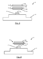
- FIG. 1 is a diagram of an illumination source according to various embodiments of the present invention.
- the illumination source 10 includes a light emitting device 12 mounted on a header 14.
- the light emitting device 12 may be a light emitting diode (LED) including a lead wire 16 that allows the LED to be biased so that it will emit light.
- the LED may emit photons in the ultraviolet and/or visible portions of the optical spectrum.
- the light emitting device 12 may be, for example, one or more lasers, one or more laser diodes, multiple LEDs, one or more lamps, or combinations thereof.
- the illumination source 10 illustrated in Figure 1 also includes, in the path of the emitted light from the light emitting device 12, an assembly 18 comprising a photoluminescent material assembly 17 and a filter 19.
- the photoluminescent material assembly 17 may comprise a photoluminescent material layer 20 placed on a substrate 22.
- the filter 19 may be between the substrate 22 and the light emitting device 12.
- Light emitted from the light emitting device 12 may pass through the filter 19 and the substrate 22, and be absorbed by the photoluminescent material layer 20.
- the photoluminescent material layer 20 may then emit light at different (e.g., longer) wavelengths than the light absorbed from the light emitting device 12.
- the light emitting device 12 may optically pump the photoluminescent material layer 20, which may convert the short wavelength photons emitted by the light emitting device 12 into longer wavelength photons.
- the photoluminescent material layer 20 may convert the short wavelength photons emitted by the light emitting device 12 into longer wavelength photons.
- the filter 19 may be constructed such that the light emitted from the photoluminescent material layer 20, which may be generally omnidirectional due to the properties of the photoluminescent material, is reflected back in a direction generally away from the light emitting device 12. That is, the filter 19 may allow the shorter wavelengths from the light emitting device 12 to pass through to the photoluminescent material layer 20, but reflect back the longer wavelengths emitted from the photoluminescent material layer 20 in a direction generally away from the light emitting device 12. This will tend to increase the efficiency of the illumination source 10 as light emitted from the photoluminescent material layer 20 may be directed in a substantially common direction.
- the photoluminescent material layer 20 may comprise quantum dot material and/or phosphors incorporated in an inert host material, such as epoxy, resin, gel, etc.
- Quantum dots have the characteristic that by adjusting the size and chemistry of the quantum dot particles, the optical properties of the material, such as light absorption or light emission, can be tailored to meet desired characteristics.
- quantum dot material which may be made from CdSe, CdS or ZnS or other materials, may have absorption in the blue and UV portion of the optical spectrum and emission wavelengths in the visible part of the optical spectrum. Phosphors can also upconvert the light emitted from the light emitting device 12.
- the substrate 22 on which the photoluminescent material layer 20 is placed may be optically transparent such that all or most of the light from light emitting device 12 passes through the substrate 22 and impinges on the photoluminescent material layer 20.
- the substrate 20 may be made from glass, such as sapphire glass.
- the inert host material comprising the photoluminescent material may be placed on the filter 19, obviating the need for a separate substrate.
- the filter 19 may be any optical device that is capable of allowing all or most of the photons from the light emitting device 12 to pass through to the photoluminescent material layer 20, but which reflects all or most of the longer-wavelength photons emitted from the photoluminescent material layer 20 in a direction generally away from the light emitting device 12.
- the light then can be collected by an optical component (See Figure 5) that may direct the light from the illumination source 10 usefully onto a target, for example.
- the filter 19 may be a dielectric filter.
- the dielectric filter may comprise multiple layers of materials with different refractive indices.
- the dielectric filter may have alternating layers of SiO 2 and TiO 2 , where SiO 2 has a low refractive index and TiO 2 has a high refractive index.
- the filter 19 can be constructed such that it will pass light with wavelengths near a target (or center) wavelength and primarily reflect all other relevant wavelengths.
- the filter 19 may be constructed such that the target (or center) wavelength corresponds to the emission spectra from the light emitting device 12.
- Other materials that may be used to construct such a dielectric filter include MgF 2 , Ta 2 O 5 , and SiN.
- the assembly 18 may be spaced-apart from the light emitting device 12 as shown in Figure 1 and may be supported by a frame (not shown), for example.
- the assembly 18 and the light emitting device 12 may additionally be encased in a casing (not shown).
- the photoluminescent material layer 20 may comprise a composite of different quantum dot intra-layers 21a-c suspended in the host material 23, as shown in Figure 2, each intra-layer 21a-c having different absorption/emission characteristics.
- the first quantum dot material intra-layer 21 a may convert a portion of the light from the light emitting device 12 to a certain, longer wavelength range
- the second quantum dot material intra-layer 21 b may convert a portion of that light to an even longer wavelength range, and so on.
- the second intra-layer 21 b may transmit the longer wavelengths emitted by the first intra-layer 21 a, and may also convert another portion of the shorter wavelengths from the light emitting device 12 to a second, higher wavelength (which may be shorter or longer than the wavelengths emitted by intra-layer 21 a), and so on.
- the thicknesses of the various quantum dot material intra-layers 21a-c could also be selected to tune the intensity of the emitted light. This may allow the illumination spectra to be further tailored to have specific features, such as multiple sharp emission peaks or broad band illumination that covers a wide range of the optical spectrum.
- one or more of the intra-layers 21 a-c may comprise phosphors rather than quantum dot material according to various embodiments.
- the illumination source 10 may comprise multiple photoluminescent material assemblies 17.
- the filter 19 may be positioned, as shown in Figure 3, between the first photoluminescent material assembly 17a and the light emitting device 12. The filter 19 may pass light from the light emitting device 12 and reflect emitted light from both of the photoluminescent material assemblies 17a-b in a common direction away from the light emitting device 12.
- the photoluminescent material layer 20a of one of the assemblies 17a may have different absorption/emission characteristics than the photoluminescent material layer 20b of the other assembly 17b. That way, for example, like the embodiment discussed above where multiple quantum dot material intra-layers 21 are suspended in a common host material, the first photoluminescent material layer 20a may convert a portion of the light from the light emitting device 12 to a certain, longer wavelength range, and the second photoluminescent material layer 20b may convert a portion of that light to an even longer wavelength range, and so on.
- the second photoluminescent material layer 20b may transmit the longer wavelengths emitted from the first photoluminescent layer 20a, and convert another portion of the shorter wavelengths emitted from the light emitting device 12 to another, longer wavelength range, which may be longer or shorter than the wavelengths from the first photoluminescent layer 20a), and so on.
- the thicknesses of the various photoluminescent material layers 20a,b could also be selected to tune the intensity of the emitted light.
- one or more of the photoluminescent material layers 20a,b may comprise a composite of different quantum dot intra-layers or phosphors suspended in the host material, each with different absorption/emission characteristics, as described above in connection with Figure 2.
- the two (or more) photoluminescent material layers 20a,b may be applied sequentially to a common substrate 22, as shown in Figure 4.
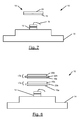
- Figure 8 shows the illumination source 10 according to another embodiment.
- the embodiment of Figure 8 is similar to that of Figure 3, except that the embodiment includes two filters 19a-b, one associated with each photoluminescent material assemblies 17a-b.
- the second filter 19b may be transmissive of light emitted by the first photoluminescent material assembly 17a and the light emitting device 12, and reflective of light emitted by the second photoluminescent material layer 20b.
- more than two photoluminescent material assemblies 17 may be used, and some or all of them may have an associated filter 19.
- the illumination source 10 may include one or more optical elements, such as a lens 24 positioned between the light emitting device 12 and the assembly 18 and/or a lens 26 after the assembly 18.
- the lens 24 may collect and focus light from the light emitting device 12 onto the assembly 18, which may provide more efficient use of the light energy from the light emitting device 12.
- the lens 26 may collimate the light exiting the assembly 18.
- the lens 26 may collect and focus light emitted from the photoluminescent material on a target sample to be illuminated by the illumination source 10. This may further enhance the efficiency of the illumination source 10.
- the light emitting device 12 may emit photons in the ultraviolet portion of the optical spectrum (wavelengths ⁇ 400 nm), and the photoluminescent material assembly 17 may convert the pump light to longer wavelengths at sufficient intensities over a broad spectrum, such as wavelengths of 400 nm to 700 nm.
- the light emitting device 12 may emit photons in the blue portion of the optical spectrum (wavelengths between 400 nm and 425 nm), and the photoluminescent material assembly 17 may emit light at sufficient intensities over the 400 nm to 700 nm range.
- the quantum dot material layer(s) 20 may be chosen such that the emission spectra of the illumination source 10 is limited to a narrow band of wavelengths.
- narrow band means less than or equal to 50 nm full width at half maximum (FWHM). That is, when the emission spectra of the illumination source 10 is a narrow band, the difference between the wavelengths at which emission intensity of the illumination source is half the maximum intensity is less than or equal to 50 nm.
- the photoluminescent material layer(s) 20 may be chosen such that the emission spectra of the illumination source corresponds to a known spectral emission standard such as, for example, incandescent standards (e.g., CIE standard illuminant A), daylight standards (e.g., CIE standard illuminant D65 or D50), fluorescent standards (e.g., CIE standard illuminant F2 or F11), or other defined standards.
- incandescent standards e.g., CIE standard illuminant A
- daylight standards e.g., CIE standard illuminant D65 or D50
- fluorescent standards e.g., CIE standard illuminant F2 or F11
- FIG. 6 is a simplified block diagram of a color measurement or spectroscopic apparatus 30 according to various embodiments of the present invention that comprises one illumination source 10 for illuminating a target material 32, a wavelength discriminating device 34, and an optical radiation sensing device 36.
- Reflected light from the target material 32 can be filtered by the wavelength discriminating device 34, which may be, for example, a prism, diffraction grating, holographic grating, or assembly of optical filters.
- the optical radiation sensing device 36 which may comprise, for example, one or a number of photodiodes, may sense the light from the material 32 passing through the wavelength discriminating device 34.
- a processor 38 in communication with the optical radiation sensing device 36 may determine the transmission, absorption, emission or reflection of the material 32.
- the system 30 may include other optical components (not shown), such as refractive or diffractive lenses or mirrors, for either directing light from the illumination source 10 onto the material 32 and/or directing light from the material 32 to the wavelength discriminating device 34.
- the wavelength discriminating device 34 and the optical radiation sensing device 36 may be positioned on the opposite side of the target material 32 from the illumination source 10. That way, the optical radiation sensing device 36 may detect light transmitted through the target material 32.
- the apparatus 30 may comprise one optical radiation sensing device in front of the target 32 for detecting light reflected by the target 32 and a second optical radiation sensing device behind the target for detecting light transmitted through the target 32.
- One or more of the illumination sources 10 could be used in other equipment, including, for example, a printing press, an ink jet printer, or other color-based process monitoring equipment.
Landscapes
- Physics & Mathematics (AREA)
- Spectroscopy & Molecular Physics (AREA)
- General Physics & Mathematics (AREA)
- Immunology (AREA)
- Biochemistry (AREA)
- Pathology (AREA)
- Health & Medical Sciences (AREA)
- Life Sciences & Earth Sciences (AREA)
- Chemical & Material Sciences (AREA)
- Analytical Chemistry (AREA)
- General Health & Medical Sciences (AREA)
- Mathematical Physics (AREA)
- Engineering & Computer Science (AREA)
- Theoretical Computer Science (AREA)
- Led Device Packages (AREA)
- Optical Filters (AREA)
- Semiconductor Lasers (AREA)
- Investigating Or Analysing Materials By Optical Means (AREA)
Applications Claiming Priority (1)
| Application Number | Priority Date | Filing Date | Title |
|---|---|---|---|
| US11/434,601 US20070262714A1 (en) | 2006-05-15 | 2006-05-15 | Illumination source including photoluminescent material and a filter, and an apparatus including same |
Publications (2)
| Publication Number | Publication Date |
|---|---|
| EP1857790A2 true EP1857790A2 (fr) | 2007-11-21 |
| EP1857790A3 EP1857790A3 (fr) | 2008-10-15 |
Family
ID=38430515
Family Applications (1)
| Application Number | Title | Priority Date | Filing Date |
|---|---|---|---|
| EP07100618A Withdrawn EP1857790A3 (fr) | 2006-05-15 | 2007-01-16 | Source d'illumination dotée d'un matériau photoluminescent et d'un filtre, et appareil l'incluant |
Country Status (3)
| Country | Link |
|---|---|
| US (1) | US20070262714A1 (fr) |
| EP (1) | EP1857790A3 (fr) |
| WO (1) | WO2007133742A2 (fr) |
Cited By (6)
| Publication number | Priority date | Publication date | Assignee | Title |
|---|---|---|---|---|
| EP2233913A1 (fr) * | 2009-03-24 | 2010-09-29 | BAM Bundesanstalt für Materialforschung und -prüfung | Standard optique destiné au calibrage et à la caractérisation de dispositifs de mesure optique |
| EP2534411A4 (fr) * | 2010-02-09 | 2014-06-11 | Sharp Kk | Lampe comprenant du phosphore, une source de rayonnement, un système optique et un puits thermique |
| EP3321649A1 (fr) * | 2016-11-10 | 2018-05-16 | Robert Bosch GmbH | Unité d'éclairage pour un microspectromètre, microspectromètre et terminal |
| EP2507545B2 (fr) † | 2010-05-12 | 2020-11-18 | OSRAM GmbH | Module d'un phare de véhicule |
| DE112016001966B4 (de) * | 2015-04-29 | 2020-12-24 | OSRAM Opto Semiconductors Gesellschaft mit beschränkter Haftung | Optoelektronische Anordnung |
| US11294228B2 (en) | 2016-03-24 | 2022-04-05 | Saturn Licensing Llc | Light-emitting device, display apparatus, and illumination apparatus |
Families Citing this family (42)
| Publication number | Priority date | Publication date | Assignee | Title |
|---|---|---|---|---|
| DE102007057671A1 (de) * | 2007-11-30 | 2009-06-04 | Osram Opto Semiconductors Gmbh | Beleuchtungsvorrichtung |
| WO2009137053A1 (fr) | 2008-05-06 | 2009-11-12 | Qd Vision, Inc. | Composants optiques, systèmes comprenant un composant optique et dispositifs associés |
| US9207385B2 (en) | 2008-05-06 | 2015-12-08 | Qd Vision, Inc. | Lighting systems and devices including same |
| WO2009151515A1 (fr) | 2008-05-06 | 2009-12-17 | Qd Vision, Inc. | Dispositifs d'éclairage à semi-conducteurs comprenant des nanoparticules semi-conductrices confinées quantiques |
| DE102009024941A1 (de) * | 2009-06-09 | 2010-12-23 | Carl Zeiss Surgical Gmbh | Beleuchtungsvorrichtung und medizinisch-optisches Beobachtungsgerät |
| KR20120062773A (ko) | 2009-08-14 | 2012-06-14 | 큐디 비젼, 인크. | 조명 장치, 조명 장치용 광학 요소, 및 방법 |
| US9827439B2 (en) | 2010-07-23 | 2017-11-28 | Biological Illumination, Llc | System for dynamically adjusting circadian rhythm responsive to scheduled events and associated methods |
| US8253336B2 (en) | 2010-07-23 | 2012-08-28 | Biological Illumination, Llc | LED lamp for producing biologically-corrected light |
| US9681522B2 (en) | 2012-05-06 | 2017-06-13 | Lighting Science Group Corporation | Adaptive light system and associated methods |
| US8743023B2 (en) | 2010-07-23 | 2014-06-03 | Biological Illumination, Llc | System for generating non-homogenous biologically-adjusted light and associated methods |
| US8841864B2 (en) | 2011-12-05 | 2014-09-23 | Biological Illumination, Llc | Tunable LED lamp for producing biologically-adjusted light |
| US8324808B2 (en) | 2010-07-23 | 2012-12-04 | Biological Illumination, Llc | LED lamp for producing biologically-corrected light |
| US9532423B2 (en) | 2010-07-23 | 2016-12-27 | Lighting Science Group Corporation | System and methods for operating a lighting device |
| US8686641B2 (en) | 2011-12-05 | 2014-04-01 | Biological Illumination, Llc | Tunable LED lamp for producing biologically-adjusted light |
| US8760370B2 (en) | 2011-05-15 | 2014-06-24 | Lighting Science Group Corporation | System for generating non-homogenous light and associated methods |
| US9024536B2 (en) | 2011-12-05 | 2015-05-05 | Biological Illumination, Llc | Tunable LED lamp for producing biologically-adjusted light and associated methods |
| US8247969B2 (en) * | 2010-09-28 | 2012-08-21 | GEM Weltronics TWN Corporation | Optical lens having fluorescent layer adapted for LED packaging structure |
| US8401231B2 (en) | 2010-11-09 | 2013-03-19 | Biological Illumination, Llc | Sustainable outdoor lighting system for use in environmentally photo-sensitive area |
| US8901850B2 (en) | 2012-05-06 | 2014-12-02 | Lighting Science Group Corporation | Adaptive anti-glare light system and associated methods |
| US9173269B2 (en) | 2011-05-15 | 2015-10-27 | Lighting Science Group Corporation | Lighting system for accentuating regions of a layer and associated methods |
| US8754832B2 (en) | 2011-05-15 | 2014-06-17 | Lighting Science Group Corporation | Lighting system for accenting regions of a layer and associated methods |
| US20130001597A1 (en) * | 2011-06-28 | 2013-01-03 | Osram Sylvania Inc. | Lighting Device Having a Color Tunable Wavelength Converter |
| US8866414B2 (en) | 2011-12-05 | 2014-10-21 | Biological Illumination, Llc | Tunable LED lamp for producing biologically-adjusted light |
| US9220202B2 (en) | 2011-12-05 | 2015-12-29 | Biological Illumination, Llc | Lighting system to control the circadian rhythm of agricultural products and associated methods |
| US9289574B2 (en) | 2011-12-05 | 2016-03-22 | Biological Illumination, Llc | Three-channel tuned LED lamp for producing biologically-adjusted light |
| US8963450B2 (en) | 2011-12-05 | 2015-02-24 | Biological Illumination, Llc | Adaptable biologically-adjusted indirect lighting device and associated methods |
| US9913341B2 (en) | 2011-12-05 | 2018-03-06 | Biological Illumination, Llc | LED lamp for producing biologically-adjusted light including a cyan LED |
| US9402294B2 (en) | 2012-05-08 | 2016-07-26 | Lighting Science Group Corporation | Self-calibrating multi-directional security luminaire and associated methods |
| US9006987B2 (en) | 2012-05-07 | 2015-04-14 | Lighting Science Group, Inc. | Wall-mountable luminaire and associated systems and methods |
| US8680457B2 (en) | 2012-05-07 | 2014-03-25 | Lighting Science Group Corporation | Motion detection system and associated methods having at least one LED of second set of LEDs to vary its voltage |
| CN104969099A (zh) | 2012-09-26 | 2015-10-07 | 8797625加拿大有限公司 | 多层光干涉滤片 |
| US9174067B2 (en) | 2012-10-15 | 2015-11-03 | Biological Illumination, Llc | System for treating light treatable conditions and associated methods |
| US9273851B2 (en) * | 2013-01-30 | 2016-03-01 | Shenzhen China Star Optoelectronics Technology Co., Ltd | Backlight module and liquid crystal display device |
| US9142732B2 (en) * | 2013-03-04 | 2015-09-22 | Osram Sylvania Inc. | LED lamp with quantum dots layer |
| US9347655B2 (en) | 2013-03-11 | 2016-05-24 | Lighting Science Group Corporation | Rotatable lighting device |
| US20140268731A1 (en) | 2013-03-15 | 2014-09-18 | Lighting Science Group Corpporation | Low bay lighting system and associated methods |
| KR102075982B1 (ko) | 2013-03-15 | 2020-02-12 | 삼성전자주식회사 | 반도체 발광소자 패키지 |
| KR102108994B1 (ko) * | 2013-08-30 | 2020-05-12 | 삼성전자주식회사 | 광 변환 소자 및 그 제조 방법, 그리고 이를 포함하는 광원 유닛 |
| KR20150033198A (ko) | 2013-09-23 | 2015-04-01 | 삼성디스플레이 주식회사 | 양자점 발광 소자 및 표시 장치 |
| US9749044B1 (en) * | 2016-04-05 | 2017-08-29 | Facebook, Inc. | Luminescent detector for free-space optical communication |
| US10546985B2 (en) * | 2017-03-28 | 2020-01-28 | Nanosys, Inc. | Method for increasing the light output of microLED devices using quantum dots |
| WO2018194609A1 (fr) * | 2017-04-20 | 2018-10-25 | Hewlett-Packard Development Company, L.P. | Compositions de construction |
Family Cites Families (10)
| Publication number | Priority date | Publication date | Assignee | Title |
|---|---|---|---|---|
| US6501091B1 (en) * | 1998-04-01 | 2002-12-31 | Massachusetts Institute Of Technology | Quantum dot white and colored light emitting diodes |
| FR2795248B1 (fr) * | 1999-06-21 | 2004-11-12 | Lprl Laboratoire De Physique D | Source monochromatique comprenant un materiau optiquement actif |
| EP1164401B1 (fr) * | 2000-06-17 | 2005-03-09 | Leica Microsystems Heidelberg GmbH | Microscope à photons dont les états quantiques sont enchevêtrés |
| JP2004537053A (ja) * | 2001-07-25 | 2004-12-09 | アプレラ コーポレイション | 電気泳動検出システムにおける時間遅延積分 |
| JP2004083653A (ja) * | 2002-08-23 | 2004-03-18 | Sharp Corp | 発光装置ならびに蛍光体およびその製造方法 |
| US6967346B2 (en) * | 2003-08-02 | 2005-11-22 | Formosa Epitaxy Incorporation | Light emitting diode structure and manufacture method thereof |
| TWI233697B (en) * | 2003-08-28 | 2005-06-01 | Genesis Photonics Inc | AlInGaN light-emitting diode with wide spectrum and solid-state white light device |
| US7081637B2 (en) * | 2003-12-10 | 2006-07-25 | Alex Waluszko | Ultraviolet lighting platform |
| TWI229465B (en) * | 2004-03-02 | 2005-03-11 | Genesis Photonics Inc | Single chip white light component |
| US7019325B2 (en) * | 2004-06-16 | 2006-03-28 | Exalos Ag | Broadband light emitting device |
-
2006
- 2006-05-15 US US11/434,601 patent/US20070262714A1/en not_active Abandoned
-
2007
- 2007-01-16 EP EP07100618A patent/EP1857790A3/fr not_active Withdrawn
- 2007-05-14 WO PCT/US2007/011546 patent/WO2007133742A2/fr not_active Ceased
Cited By (12)
| Publication number | Priority date | Publication date | Assignee | Title |
|---|---|---|---|---|
| EP2233913A1 (fr) * | 2009-03-24 | 2010-09-29 | BAM Bundesanstalt für Materialforschung und -prüfung | Standard optique destiné au calibrage et à la caractérisation de dispositifs de mesure optique |
| US7919744B2 (en) | 2009-03-24 | 2011-04-05 | Bam Bundesanstalt Fuer Materialforschung Und Pruefung | Optical standard for the calibration and characterization of optical measuring devices |
| EP2534411A4 (fr) * | 2010-02-09 | 2014-06-11 | Sharp Kk | Lampe comprenant du phosphore, une source de rayonnement, un système optique et un puits thermique |
| EP2507545B2 (fr) † | 2010-05-12 | 2020-11-18 | OSRAM GmbH | Module d'un phare de véhicule |
| DE112016001966B4 (de) * | 2015-04-29 | 2020-12-24 | OSRAM Opto Semiconductors Gesellschaft mit beschränkter Haftung | Optoelektronische Anordnung |
| US11294228B2 (en) | 2016-03-24 | 2022-04-05 | Saturn Licensing Llc | Light-emitting device, display apparatus, and illumination apparatus |
| EP3435429B1 (fr) * | 2016-03-24 | 2022-10-26 | Sony Group Corporation | Dispositif électroluminescent, appareil d'affichage et appareil d'éclairage |
| US11630344B2 (en) | 2016-03-24 | 2023-04-18 | Saturn Licensing Llc | Light-emitting device, display apparatus, and illumination apparatus |
| US12372827B2 (en) | 2016-03-24 | 2025-07-29 | Saturn Licensing Llc | Light-emitting device, display apparatus, and illumination apparatus |
| US12386221B2 (en) | 2016-03-24 | 2025-08-12 | Saturn Licensing Llc | Light-emitting device, display apparatus, and illumination apparatus |
| EP3321649A1 (fr) * | 2016-11-10 | 2018-05-16 | Robert Bosch GmbH | Unité d'éclairage pour un microspectromètre, microspectromètre et terminal |
| CN108072609A (zh) * | 2016-11-10 | 2018-05-25 | 罗伯特·博世有限公司 | 用于微型光谱仪的照明单元、微型光谱仪和移动终端设备 |
Also Published As
| Publication number | Publication date |
|---|---|
| US20070262714A1 (en) | 2007-11-15 |
| WO2007133742A2 (fr) | 2007-11-22 |
| EP1857790A3 (fr) | 2008-10-15 |
| WO2007133742A3 (fr) | 2008-09-18 |
Similar Documents
| Publication | Publication Date | Title |
|---|---|---|
| EP1857790A2 (fr) | Source d'illumination dotée d'un matériau photoluminescent et d'un filtre, et appareil l'incluant | |
| EP1857789A2 (fr) | Source de lumière incluant un matériau de points quantiques et appareil l'incluant | |
| US9528876B2 (en) | Solid state broad band near-infrared light source | |
| CN101784940B (zh) | 照明设备 | |
| CN208091919U (zh) | 一种荧光检测装置 | |
| US9885813B2 (en) | Projection apparatus | |
| US9239133B2 (en) | High brightness solid state illumination system for fluorescence imaging and analysis | |
| WO2006011571A1 (fr) | Source de lumière et endoscope équipé de cette source de lumière | |
| KR20100118149A (ko) | 발광 다이오드 장치 | |
| KR20090127377A (ko) | 분광 광도계 및 측정 방법 | |
| CN101821661A (zh) | 发光设备 | |
| US7456955B2 (en) | Spectrophotometer with light emitting diode illuminator | |
| JP6207359B2 (ja) | 照明装置、イメージセンサユニットおよび紙葉類識別装置 | |
| JP2014086681A (ja) | 紫外線発光装置 | |
| JP7041485B2 (ja) | ライン光源及びこれを備えた光ラインセンサユニット | |
| CN216386744U (zh) | 光源装置 | |
| CN109143596A (zh) | 一种基于棱镜结构的多光谱光源 | |
| CN208780918U (zh) | 一种基于棱镜结构的多光谱光源 | |
| US20240201076A1 (en) | Lighting assembly and method for providing measuring light and optical measuring device | |
| WO2008139363A2 (fr) | Système comprenant une source de rayonnement infrarouge et un capteur de rayonnement infrarouge | |
| CN116540398B (zh) | 一种波长转换装置及光源装置 | |
| EP4471880A1 (fr) | Dispositif électroluminescent et système de détection | |
| CN215492063U (zh) | 光源装置 | |
| RU76700U1 (ru) | Устройство подсветки шкалы прибора авиатранспортного средства | |
| HK40105416A (zh) | 用於提供测量光的照明组件和方法以及光学测量装置 |
Legal Events
| Date | Code | Title | Description |
|---|---|---|---|
| PUAI | Public reference made under article 153(3) epc to a published international application that has entered the european phase |
Free format text: ORIGINAL CODE: 0009012 |
|
| AK | Designated contracting states |
Kind code of ref document: A2 Designated state(s): AT BE BG CH CY CZ DE DK EE ES FI FR GB GR HU IE IS IT LI LT LU LV MC NL PL PT RO SE SI SK TR |
|
| AX | Request for extension of the european patent |
Extension state: AL BA HR MK YU |
|
| PUAL | Search report despatched |
Free format text: ORIGINAL CODE: 0009013 |
|
| AK | Designated contracting states |
Kind code of ref document: A3 Designated state(s): AT BE BG CH CY CZ DE DK EE ES FI FR GB GR HU IE IS IT LI LT LU LV MC NL PL PT RO SE SI SK TR |
|
| AX | Request for extension of the european patent |
Extension state: AL BA HR MK RS |
|
| AKX | Designation fees paid | ||
| REG | Reference to a national code |
Ref country code: DE Ref legal event code: 8566 |
|
| STAA | Information on the status of an ep patent application or granted ep patent |
Free format text: STATUS: THE APPLICATION IS DEEMED TO BE WITHDRAWN |
|
| 18D | Application deemed to be withdrawn |
Effective date: 20090416 |