EP1857873A2 - Unité d'éclairage d'une caméra - Google Patents
Unité d'éclairage d'une caméra Download PDFInfo
- Publication number
- EP1857873A2 EP1857873A2 EP07008730A EP07008730A EP1857873A2 EP 1857873 A2 EP1857873 A2 EP 1857873A2 EP 07008730 A EP07008730 A EP 07008730A EP 07008730 A EP07008730 A EP 07008730A EP 1857873 A2 EP1857873 A2 EP 1857873A2
- Authority
- EP
- European Patent Office
- Prior art keywords
- functional element
- optical functional
- optoelectronic sensor
- sensor according
- light
- Prior art date
- Legal status (The legal status is an assumption and is not a legal conclusion. Google has not performed a legal analysis and makes no representation as to the accuracy of the status listed.)
- Withdrawn
Links
Images
Classifications
-
- G—PHYSICS
- G03—PHOTOGRAPHY; CINEMATOGRAPHY; ANALOGOUS TECHNIQUES USING WAVES OTHER THAN OPTICAL WAVES; ELECTROGRAPHY; HOLOGRAPHY
- G03B—APPARATUS OR ARRANGEMENTS FOR TAKING PHOTOGRAPHS OR FOR PROJECTING OR VIEWING THEM; APPARATUS OR ARRANGEMENTS EMPLOYING ANALOGOUS TECHNIQUES USING WAVES OTHER THAN OPTICAL WAVES; ACCESSORIES THEREFOR
- G03B15/00—Special procedures for taking photographs; Apparatus therefor
- G03B15/02—Illuminating scene
- G03B15/03—Combinations of cameras with lighting apparatus; Flash units
-
- H—ELECTRICITY
- H04—ELECTRIC COMMUNICATION TECHNIQUE
- H04N—PICTORIAL COMMUNICATION, e.g. TELEVISION
- H04N23/00—Cameras or camera modules comprising electronic image sensors; Control thereof
- H04N23/56—Cameras or camera modules comprising electronic image sensors; Control thereof provided with illuminating means
Definitions
- the invention relates to an optoelectronic sensor for non-contact detection of objects according to the preamble of claim 1.
- Such sensors are used, for example, in a manufacturing process to detect the presence of an object within a range can. This recognition is often associated with other functions such as a positionally accurate position detection, a sorting or selection function, etc.
- the object is illuminated with a lighting device, thereby detecting the object reflected or remitted light with a recording system.
- the recording system consists of a receiving objective and a light receiving unit arranged in its image plane.
- the light receiving unit consists of one or more photosensitive elements.
- such a recording system may consist of a simple light barrier with, for example, a single position-sensitive light-receiving unit or a digital camera.
- the light receiving unit is usually a matrix arrangement of a plurality of photosensitive elements, which are constructed in CMOS or CCD technology.
- a suitable evaluation system for image processing is usually connected downstream.
- the lighting devices known from the prior art are, for example, equipped with incandescent lamps, LEDs or lamps equipped with laser sources, the light of which is also partially directed to the objects with conventional lenses or glass fibers.
- light is not limited to the visible light. Under “light” are generally electromagnetic radiation, ie UV light, IR light and visible light to understand, which can usually be used for the operation of optoelectronic sensors.
- Such known in the art optoelectronic sensors often have problems in the application, when objects whose surface has a high gloss ratio to be reliably detected.
- the problems are due to the fact that when a high gloss object on the surface is illuminated with a directional light beam, the reflected light can be reflected by the gloss level of the object in a direction that is outside the aperture of the receiving lens.
- the image contents, which are assigned to the gloss component of the object are dark on the light receiving unit and thus can not be evaluated or only conditionally evaluated.
- the resulting hot spots reduce the image quality such that the detection performance of the optoelectronic sensor is greatly reduced.
- a dome lighting In a dome lighting, the object to be illuminated is enclosed by a nearly hemispherical hood. This hemispherical hood is covered on its inner surface with a diffusely reflecting surface layer.
- a plurality of wide-scattering light sources are arranged, which in particular illuminate the inner wall of the hemispherical hood and thus also the object. In this way, the object is illuminated from a large solid angle range out.
- This, for the illumination of the object itself good dome illumination brings in practical use several disadvantages. So in particular the large height of Disadvantage that severely limits the space between the sensor and the object plane.
- Another disadvantage of this dome lighting is to be seen in that such a large lighting device can no longer be meaningfully integrated with the recording system to form a unit.
- the invention is therefore based on the object, with a flat as possible lighting device that is inherently connected to the recording system, a object located in the object level allows diffuse lighting from a large solid angle range out.
- an optoelectronic sensor for non-contact detection of objects or object features which has a recording system with a receiving lens and a light receiving unit.
- an incident light illumination device is inherently connected to the recording system in this sensor, with which the object plane is illuminated.
- the inherent incident illumination device in its outer shape has substantially the shape of a flat disc which surrounds the receiving lens rotationally symmetrical.
- the epi-illumination device has a central opening through which the light reflected from the object can enter the receiving objective.
- the receiving system and incident light illumination device form a compact unit in which the required electrical supply and data lines of the two components are combined in an advantageous manner.
- an optical functional element adapted to the size of the outer shape is coupled in whose boundary surface, which faces away from the object, several light sources to emit their emitted light and the light emerges uniformly distributed from the boundary surface facing the object Object level illuminated with homogeneous luminous intensity distribution. It is particularly advantageous if the outer diameter of the optical functional element is often greater than the effective aperture diameter of the receiving lens, because thereby also the surface portions of an object, which are arranged greatly inclined to the optical axis of the receiving lens, the entire field of vision still well.
- the light emerging from the optical functional element illuminates the object plane in a diffuse manner, because thereby possible highlights on the object do not cause any recognition errors due to dark zones or hot spots in the image plane.
- the light sources without an air gap, that is connected via a suitable optical contact means with the optical functional element. In this way, there are no optical interfaces between, for example, an LED and the optical functional element, so that thereby the coupling efficiency of the light from the LED into the optical functional element is increased.
- the light sources are connected via a detachable connection with the optical functional element. This embodiment is particularly advantageous if, for example, the optical functional elements for the purpose of adaptation to different object distances or to change the size of the illuminated area in the object plane to be replaced.
- An advantageous embodiment of the rear optical interface of the optical functional element provides that this at least partially has a location-dependent surface profile.
- This location-dependent surface profile can be formed from lenses, wedge surfaces or course surfaces. It is also intended to carry out these elements in microform, Fresnel or as diffractive elements. With such a surface profile on the rear optical interface, it is possible to selectively influence the course of the injected light by scattering and / or by distractions. It is furthermore advantageous if the optical functional element on the rear optical interface is at least partially provided with a mirror layer. In this way, the light coupled in the functional element, which impinges on the boundary surface at a smaller angle than the limiting angle of the total reflection coming from the inside, can be held in the functional element.
- a further embodiment of the invention provides that the optical functional element is at least partially provided with a non-metallic coating or printing on the rear boundary surface. With these partially different thick or dense coatings / prints, it is possible that the homogeneity of the light distribution at the light exit from the functional element is advantageously influenced within wide limits. Analogous to the design forms for the rear interface of the optical functional element, it is provided in further advantageous embodiments of the invention, alternatively or simultaneously, to provide the surface of the optical functional element indicative of the object plane with a profiling and / or coating or printing. Moreover, it is advantageous if the optical functional element has a significantly larger area fraction than the illuminated object plane.
- an object that is located in the object plane is illuminated from a large solid angle range.
- a homogenization of the light distribution can also be achieved according to the invention in an advantageous manner in that the optical functional element is made of a material which has at least partially a volume scattering.
- the material for the optical functional element which consists for example of polycarbonate, glass fiber shares still admixed. It can also be regarded as advantageous if the optical functional element has rotationally symmetrical different thickness.
- the inherently flat optical functional element can have a greater material thickness in its central region and thus have the shape of a cone with a very blunt cone angle. Furthermore, it is also provided that one or both of the boundary surfaces of the optical functional element have a slightly spherical, asnoswitz or spline curve. With these geometric variants in the shape of the functional element is possible to influence not only the homogenization of the light distribution but also the emission direction of the light between the functional element and the illuminated object plane. From the point of view of a cost-effective and small-volume design, it is advantageous if the light sources are arranged annularly in the middle region directly around the receiving lens. In this case, for example, the LEDs are all arranged on a disc-shaped circuit board, whereby the electrical Wiring costs within the inherent incident illumination device is significantly minimized.
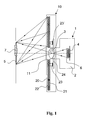
- FIGURE shows a schematic view of an optoelectronic sensor with a pick-up system and incident-light illumination device.
- the optoelectronic sensor shown in Fig. 1 has a recording system 1, which has a receiving objective 3 and a light receiving unit 4 in a housing 2.
- This light receiving unit 4 may consist of a single photosensitive element or, as shown in Fig. 1, a plurality of photosensitive elements constructed in CMOS or CCD technology.
- the reception objective 3 from the recording system 1 an image of an object plane 5 on the surface 6 of the light receiving unit 4 is generated.
- the light receiving unit 4 consists of a matrix-shaped two-dimensional light receiver, as known from a digital camera, the image can be read out from the object plane 5 and fed to an image processing unit, not shown here. If, as also shown in FIG.
- an object 7 is located in the object plane 5, in particular the features of the object surface on the surface 6 of the light receiving unit 4 are reproduced by the object 7.
- the recording system 1 is provided with an inherent incident illumination device 10.
- This incident illumination device 10 has in its outer shape substantially the shape of a flat disc with a central opening 11. Through this central opening 11 through the receiving system 1 can take the image of the object plane 5.
- the main component in the incident illumination device 10 is an optical functional element 20 having a rear optical interface 21 and an object plane indicative interface 22.
- a plurality of light sources 23, 23 ' shown here in the form of LEDs. on a circuit board 24 arranged.
- the light emitted by the light sources 23 is coupled directly into the optical functional element 20.
- the light sources 23 can be fixedly connected to the optical functional element 20 via an optical contact means, or the light sources 23 couple their light into the optical functional element 20 via a small air gap.
- the rear optical interface 21 and / or the surface 22 indicative of the object plane are provided with a location-dependent surface profile (not shown in detail). Depending on the task, this surface profile is composed of several different types of optical elements.
- the optical interface 21 and / or the boundary surface 22 indicative of the object plane is partially provided with a location-dependent mirror layer and / or an imprint.
- a volume-scattering material is used as the material for the optical functional element 20.
- the two boundary surfaces 21 and 22 of the optical functional element 20 have a slightly spherical, aspherical or spline curve.
Landscapes
- Physics & Mathematics (AREA)
- General Physics & Mathematics (AREA)
- Engineering & Computer Science (AREA)
- Multimedia (AREA)
- Signal Processing (AREA)
- Photo Coupler, Interrupter, Optical-To-Optical Conversion Devices (AREA)
- Photometry And Measurement Of Optical Pulse Characteristics (AREA)
- Geophysics And Detection Of Objects (AREA)
Applications Claiming Priority (1)
| Application Number | Priority Date | Filing Date | Title |
|---|---|---|---|
| DE102006023142A DE102006023142A1 (de) | 2006-05-16 | 2006-05-16 | Kamera-Beleuchtungseinheit |
Publications (2)
| Publication Number | Publication Date |
|---|---|
| EP1857873A2 true EP1857873A2 (fr) | 2007-11-21 |
| EP1857873A3 EP1857873A3 (fr) | 2013-07-10 |
Family
ID=38331690
Family Applications (1)
| Application Number | Title | Priority Date | Filing Date |
|---|---|---|---|
| EP07008730.9A Withdrawn EP1857873A3 (fr) | 2006-05-16 | 2007-04-28 | Unité d'éclairage d'une caméra |
Country Status (2)
| Country | Link |
|---|---|
| EP (1) | EP1857873A3 (fr) |
| DE (1) | DE102006023142A1 (fr) |
Cited By (1)
| Publication number | Priority date | Publication date | Assignee | Title |
|---|---|---|---|---|
| EP3026470A1 (fr) * | 2009-10-30 | 2016-06-01 | Fujitsu Frontech Limited | Plaque à prismes, système optique d'éclairage de dispositif d'imagerie et matrice de formation de plaque à prismes |
Families Citing this family (3)
| Publication number | Priority date | Publication date | Assignee | Title |
|---|---|---|---|---|
| DE102011008328B4 (de) * | 2011-01-11 | 2022-03-17 | Baumer Electric Ag | Optischer Sensor mit gefärbter Frontscheibe |
| DE102013105105B3 (de) * | 2013-05-17 | 2014-11-06 | Sick Ag | 3D-Kamera mit mindestens einer Beleuchtungsvorrichtung |
| DE202013102178U1 (de) | 2013-05-17 | 2014-08-18 | Sick Ag | Beleuchtungsvorrichung zur Erzeugung eines Beleuchtungsbereichs für eine 3D-Kamera |
Family Cites Families (11)
| Publication number | Priority date | Publication date | Assignee | Title |
|---|---|---|---|---|
| US3474242A (en) * | 1966-10-14 | 1969-10-21 | David W Forrant | Photographic ring light |
| US5690417A (en) * | 1996-05-13 | 1997-11-25 | Optical Gaging Products, Inc. | Surface illuminator with means for adjusting orientation and inclination of incident illumination |
| JP3118503B2 (ja) * | 1996-07-08 | 2000-12-18 | シーシーエス株式会社 | 照明装置 |
| TW402856B (en) * | 1996-12-26 | 2000-08-21 | Palite Corp | LED illuminator |
| US6022124A (en) * | 1997-08-19 | 2000-02-08 | Ppt Vision, Inc. | Machine-vision ring-reflector illumination system and method |
| US6429934B1 (en) * | 1998-09-11 | 2002-08-06 | Robotic Vision Systems, Inc. | Optimal symbology illumination-apparatus and method |
| DE10026301A1 (de) * | 2000-05-26 | 2001-11-29 | Sick Ag | Verfahren und Vorrichtung zur Bildverarbeitung |
| WO2002073953A2 (fr) * | 2001-03-08 | 2002-09-19 | Hand Held Products, Inc. | Module d'imagerie de lecteur optique |
| US6791736B2 (en) * | 2001-06-19 | 2004-09-14 | Teralum Llc | Optical device for dispersion compensation |
| US20030161024A1 (en) * | 2002-02-27 | 2003-08-28 | Qin Zhang | Dual fibers coupled to an etalon |
| WO2005031392A2 (fr) * | 2003-09-26 | 2005-04-07 | Ramot At Tel-Aviv University Ltd. | Reflecteur a microlentille et coupleur lumineux integre |
-
2006
- 2006-05-16 DE DE102006023142A patent/DE102006023142A1/de not_active Withdrawn
-
2007
- 2007-04-28 EP EP07008730.9A patent/EP1857873A3/fr not_active Withdrawn
Cited By (1)
| Publication number | Priority date | Publication date | Assignee | Title |
|---|---|---|---|---|
| EP3026470A1 (fr) * | 2009-10-30 | 2016-06-01 | Fujitsu Frontech Limited | Plaque à prismes, système optique d'éclairage de dispositif d'imagerie et matrice de formation de plaque à prismes |
Also Published As
| Publication number | Publication date |
|---|---|
| EP1857873A3 (fr) | 2013-07-10 |
| DE102006023142A1 (de) | 2007-11-22 |
Similar Documents
| Publication | Publication Date | Title |
|---|---|---|
| DE69931503T2 (de) | Vorrichtung und verfahren zur diffusen beleuchtung einer oberfläche | |
| DE112008001114B4 (de) | Vorrichtung für die Oberflächenprüfung | |
| DE69829886T2 (de) | Vorrichtung zum Lesen eines optischen Codes | |
| EP1991450B1 (fr) | Ensemble caméra pour véhicule à moteur | |
| DE19526512B4 (de) | Beleuchtungsvorrichtung für Fahrzeuge | |
| DE112015002290T5 (de) | Abbildungsmodul, lesegerät und verfahren zum beleuchten und abbilden von zielen, die über einen erweiterten bereich von arbeitsabständen gelesen werden sollen | |
| DE102008044003A1 (de) | Kameramodul mit Mehrfachfunktion | |
| AT500056A1 (de) | Optikelement für verkehrszeichen, anzeigetafeln oder dgl. | |
| DE112013006158T5 (de) | Lichtleiter, Lichtquellenvorrichtung und Bildleseeinrichtung | |
| DE10219246A1 (de) | Beleuchtungseinrichtung für Kraftfahrzeuge | |
| EP1730500B1 (fr) | Systemes optiques pour la production d'une bande d'eclairage | |
| DE102019116965B4 (de) | Ein Licht leitendes optisches System, insbesondere für Kraftfahrzeuge | |
| DE102010038186A1 (de) | Optoelektronischer Sensor mit Linienanordnung von Einzelemittern | |
| EP1727678B1 (fr) | Systeme optique de production d'une forme eclairee | |
| DE102013225950A1 (de) | Kraftfahrzeugbeleuchtungseinrichtung | |
| DE19511197C2 (de) | Verfahren und Vorrichtung zum optischen Prüfen einer Oberfläche, insbesondere einer Compact-Disc | |
| EP1857873A2 (fr) | Unité d'éclairage d'une caméra | |
| EP1892495B1 (fr) | Dispositif et procédé destinés à l'évaluation des impacts du tir | |
| EP2513874B1 (fr) | Détecteur pour vérifier des documents de valeur | |
| DE10159234B4 (de) | Vorrichtung zur Untersuchung von Dokumenten | |
| DE10323409A1 (de) | Vorrichtung zur Prüfung von Banknoten | |
| WO2015135676A1 (fr) | Dispositif d'acquisition d'images notamment pour le contrôle de la géométrie des trains roulants | |
| DE69029550T2 (de) | Vorrichtung zum optischen Abtasten eines Dokuments | |
| EP3028101A1 (fr) | Ensemble optique pour vue panoramique | |
| DE10244767A1 (de) | Verfahren und Vorrichtung zum Bestimmen des Abstands zwischen einer Referenzebene und einer inneren oder äußeren optischen Grenzfläche eines Objekts sowie Verwendung derselben zum Bestimmen eines Oberflächenprofils eines, inbesondere metallischen, Objekts, Autofokus-Modul, Mikroskop und Verfahren zum Autofokussieren eines Mikroskops |
Legal Events
| Date | Code | Title | Description |
|---|---|---|---|
| PUAI | Public reference made under article 153(3) epc to a published international application that has entered the european phase |
Free format text: ORIGINAL CODE: 0009012 |
|
| AK | Designated contracting states |
Kind code of ref document: A2 Designated state(s): AT BE BG CH CY CZ DE DK EE ES FI FR GB GR HU IE IS IT LI LT LU LV MC MT NL PL PT RO SE SI SK TR |
|
| AX | Request for extension of the european patent |
Extension state: AL BA HR MK YU |
|
| PUAL | Search report despatched |
Free format text: ORIGINAL CODE: 0009013 |
|
| AK | Designated contracting states |
Kind code of ref document: A3 Designated state(s): AT BE BG CH CY CZ DE DK EE ES FI FR GB GR HU IE IS IT LI LT LU LV MC MT NL PL PT RO SE SI SK TR |
|
| AX | Request for extension of the european patent |
Extension state: AL BA HR MK RS |
|
| RIC1 | Information provided on ipc code assigned before grant |
Ipc: G03B 15/03 20060101AFI20130605BHEP Ipc: H04N 5/225 20060101ALI20130605BHEP |
|
| STAA | Information on the status of an ep patent application or granted ep patent |
Free format text: STATUS: THE APPLICATION HAS BEEN WITHDRAWN |
|
| 18W | Application withdrawn |
Effective date: 20130723 |