EP1858057A2 - Dispositif luminescent avec des des couches de luminophores excitées par d'éléctrons, et dispositif d'affichage utilisant le dispositif luminescent comme source de lumière - Google Patents
Dispositif luminescent avec des des couches de luminophores excitées par d'éléctrons, et dispositif d'affichage utilisant le dispositif luminescent comme source de lumière Download PDFInfo
- Publication number
- EP1858057A2 EP1858057A2 EP07108201A EP07108201A EP1858057A2 EP 1858057 A2 EP1858057 A2 EP 1858057A2 EP 07108201 A EP07108201 A EP 07108201A EP 07108201 A EP07108201 A EP 07108201A EP 1858057 A2 EP1858057 A2 EP 1858057A2
- Authority
- EP
- European Patent Office
- Prior art keywords
- light emission
- emission device
- substrate
- heat dissipation
- electrodes
- Prior art date
- Legal status (The legal status is an assumption and is not a legal conclusion. Google has not performed a legal analysis and makes no representation as to the accuracy of the status listed.)
- Withdrawn
Links
Images


Classifications
-
- G—PHYSICS
- G02—OPTICS
- G02F—OPTICAL DEVICES OR ARRANGEMENTS FOR THE CONTROL OF LIGHT BY MODIFICATION OF THE OPTICAL PROPERTIES OF THE MEDIA OF THE ELEMENTS INVOLVED THEREIN; NON-LINEAR OPTICS; FREQUENCY-CHANGING OF LIGHT; OPTICAL LOGIC ELEMENTS; OPTICAL ANALOGUE/DIGITAL CONVERTERS
- G02F1/00—Devices or arrangements for the control of the intensity, colour, phase, polarisation or direction of light arriving from an independent light source, e.g. switching, gating or modulating; Non-linear optics
- G02F1/01—Devices or arrangements for the control of the intensity, colour, phase, polarisation or direction of light arriving from an independent light source, e.g. switching, gating or modulating; Non-linear optics for the control of the intensity, phase, polarisation or colour
- G02F1/13—Devices or arrangements for the control of the intensity, colour, phase, polarisation or direction of light arriving from an independent light source, e.g. switching, gating or modulating; Non-linear optics for the control of the intensity, phase, polarisation or colour based on liquid crystals, e.g. single liquid crystal display cells
- G02F1/133—Constructional arrangements; Operation of liquid crystal cells; Circuit arrangements
- G02F1/1333—Constructional arrangements; Manufacturing methods
- G02F1/1335—Structural association of cells with optical devices, e.g. polarisers or reflectors
-
- H—ELECTRICITY
- H01—ELECTRIC ELEMENTS
- H01J—ELECTRIC DISCHARGE TUBES OR DISCHARGE LAMPS
- H01J63/00—Cathode-ray or electron-stream lamps
- H01J63/02—Details, e.g. electrode, gas filling, shape of vessel
-
- H—ELECTRICITY
- H01—ELECTRIC ELEMENTS
- H01J—ELECTRIC DISCHARGE TUBES OR DISCHARGE LAMPS
- H01J63/00—Cathode-ray or electron-stream lamps
- H01J63/06—Lamps with luminescent screen excited by the ray or stream
-
- B—PERFORMING OPERATIONS; TRANSPORTING
- B82—NANOTECHNOLOGY
- B82Y—SPECIFIC USES OR APPLICATIONS OF NANOSTRUCTURES; MEASUREMENT OR ANALYSIS OF NANOSTRUCTURES; MANUFACTURE OR TREATMENT OF NANOSTRUCTURES
- B82Y40/00—Manufacture or treatment of nanostructures
-
- H—ELECTRICITY
- H01—ELECTRIC ELEMENTS
- H01J—ELECTRIC DISCHARGE TUBES OR DISCHARGE LAMPS
- H01J61/00—Gas-discharge or vapour-discharge lamps
- H01J61/02—Details
- H01J61/30—Vessels; Containers
- H01J61/305—Flat vessels or containers
Definitions
- the present invention relates to a display device, and more particularly, to a light emission device for emitting light using electron emission regions and a phosphor layer, and a display device using the light emission device as a light source.
- a light emission device that includes front and rear substrates facing each other with a gap therebetween, a plurality of electron emission regions provided on the rear substrate, and a phosphor layer and an anode electrode provided on the front substrate is well known.
- the light emission device has a simplified optical member and lower power consumption than both a cold cathode fluorescent lamp (CCFL) type light emission device and a light emitting diode (LED) type light emission device.
- CCFL cold cathode fluorescent lamp
- LED light emitting diode
- the rear and front substrates are sealed together at their peripheries using a sealing member to form a vacuum vessel.
- a sealing member to form a vacuum vessel.
- electrons emitted from the electron emission regions are accelerated toward the phosphor layer by an anode voltage applied to the anode electrode, and excite the phosphor layer to emit visible light.
- the luminance of a light emission surface is proportional to the anode voltage.
- the light emission device can be used as a light source in a display device including a non-self emissive type display panel.
- a large amount of heat is generated from the front substrate by the continuous electron collision with the phosphor layer.
- the front substrate is disposed facing the display panel, it is very difficult to install a cooling device. Therefore, the heat generated from the front substrate causes the deterioration of not only the performance of the display panel but also of the light emission efficiency of the phosphor layer that is exposed to the heat for a long time.
- the light emission device is driven so as to maintain a predetermined brightness all the entire light emission surface when the display device is driven. Therefore, it is difficult to improve the display quality to a sufficient level.
- Exemplary embodiments in accordance with the present invention provide a light emission device that can dissipate the heat generated from a front substrate and a display device, which uses the light emission device as a light source to reduce or prevent the performance deterioration of a display panel.
- Exemplary embodiments in accordance with the present invention also provide a light emission device that can independently control light intensities of a plurality of divided regions of a light emission surface and a display device that can enhance the dynamic contrast of the screen by using the light emission device as a light source.
- a light emission device includes: first and second substrates facing each other and forming a vacuum vessel; an electron emission unit located on the first substrate; and a light emission unit located on the second substrate.
- the light emission unit includes a plurality of phosphor layers located on the second substrate and spaced from each other, a heat dissipation layer located between the phosphor layers and having an end extending to outside of the vacuum vessel to be exposed to air, and an anode electrode located at one side of the phosphor layers and the heat dissipation layer.
- the heat dissipation layer comprises a material having a thermal conductivity between 0.1 cal/cm ⁇ s ⁇ °C and 1.0 cal/cm.s.°C, more preferably the heat dissipation layer comprises a material having a thermal conductivity between 0.1 cal/cm ⁇ s ⁇ °C and 0.3 cal/cm ⁇ s ⁇ °C or between 0.49 cal/cm.s.°C and 1.0 cal/cm.s.°C.
- the heat dissipation layer may be formed of a carbon-based conductive material.
- the heat dissipation layer may be formed of carbon-based conductive material such as graphite.
- the heat dissipation layer may include a metal selected from the group consisting of Al, Ag, Cu, Au, Pt, and an alloy thereof.
- the thickness of the heat dissipation layer is the same as the thickness of the phosphor layer.
- the ratio between the thickness of the heat dissipation layer and the thickness of the phosphor layer may range from 0.9 to 1.1.
- each of the phosphor layers is formed in a tetragonal shape (for example in a rectangular pattern) and the heat dissipation layer is formed in a lattice pattern.
- the anode electrode may include a metal layer located on the phosphor layers and the heat dissipation layer at a side facing the first substrate.
- the anode electrode may include a transparent conductive layer located on the phosphor layers and the heat dissipation layer at a side facing the second substrate.
- a metal layer may be located on the phosphor layers and the heat dissipation layer at a side facing the first substrate.
- the electron emission unit may include first and second electrodes insulated from each other and crossing each other and electron emission regions electrically connected to one of the first electrodes or the second electrodes.
- the electron emission regions include at least one of a carbon-based material or a nanometer-sized material (i.e. particles having a size in the range of 1nm and 1000nm).
- a display device includes: a display panel for displaying an image; a light emission device for emitting light toward the display panel.
- the light emission device includes: first and second substrates facing each other and forming a vacuum vessel; an electron emission unit located on the first substrate; and a light emission unit including a plurality of phosphor layers located on the second substrate and spaced from each other, a heat dissipation layer located between the phosphor layers and having an end extending to outside of the vacuum vessel to be exposed to air, and an anode electrode located at one side of the phosphor layers and the heat dissipation layer.
- the display panel includes first pixels and the light emission device includes second pixels.
- the number of the second pixels may be less than that of the first pixels and light emission intensities of the second pixels may be independently controlled.
- the display panel may be a liquid crystal display panel.
- the electron emission unit may include first electrodes and second electrodes crossing the first electrodes, wherein the first electrodes are insulated from the second electrodes; and electron emission regions electrically connected to the first electrodes or the second electrodes.
- the electron emission regions may include a material that emits electrons in response to an electric field.
- the electron emission regions may include at least one of a carbon-based material or a nanometer-sized material.
- a diffuser for uniformly diffusing the light emitted from the light emission device toward the display panel (liquid crystal display panel) may be disposed between the display panel (liquid crystal display panel) and the light emission device.
- the diffuser is spaced apart from the light emission device by a predetermined distance ranging from 1 mm to 20mm.
- no cooling device is arranged between the display panel and the light emission device.
- FIG. 1 is a sectional view of a light emission device according to an embodiment of the present invention.
- a light emission device 10 of the present embodiment includes first and second substrates 12 and 14 facing each other with a predetermined distance between them.
- a sealing member 16 is provided at the peripheries of the first and second substrates 12 and 14 to seal them together and thus form a sealed vessel.
- the interior of the sealed vessel is kept to a degree of vacuum of about 10 -6 Torr.
- the substrates 12, 14 and the sealing member 16 can be said to form a vacuum envelope (or a vacuum vessel).
- Each of the first and second substrates 12 and 14 has an active area emitting visible light and an inactive area surrounding the active area within an area surrounded by the sealing member 16.
- An electron emission unit 18 for emitting electrons is provided on the active area of the first substrate 12, and a light emission unit 20 for emitting the visible light is provided on the active area of the second substrate 14.
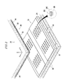
- FIG. 2 is a partial exploded perspective view of an active area of the light emission device of FIG. 1.
- the electron emission unit 18 includes first electrodes 22 and second electrodes 26 insulated from each other by an insulating layer 24 and electron emission regions 28 electrically connected to the first electrodes 22.
- the electron emission regions 28 may be electrically connected to the second electrodes 26.
- the first electrodes 22 are cathode electrodes for applying a current to the electron emission regions 28 and the second electrodes 26 are gate electrodes for inducing the electron emission by forming the electric field around the electrode emission regions 28 according to a voltage difference between the cathode and gate electrodes.
- the second electrodes 26 are the cathode electrodes and the first electrodes 22 are the gate electrodes.
- the electrodes arranged along rows of the light emission device 10 function as scan electrodes and the electrodes arranged along columns function as data electrodes.
- the first electrodes 22 are arranged along the columns (i.e., in a direction of a y-axis in FiGs. 1 and 2) of the light emission device 10
- the second electrodes 26 are arranged along the rows (i.e., in a direction of an x-axis in FIGs. 1 and 2) of the light emission device 10 is illustrated.
- the arrangements of the electron emission regions 28 and the first and second electrodes 22 and 26 are not limited to the above case.
- Openings 241 and 261 are respectively formed through the insulating layer 24 and the second electrodes 26 at crossed regions of the first and second electrodes 22 and 26 to partly expose the surface of the first electrodes 22.
- the electron emission regions 28 are formed on the first electrodes 22 through the openings 241 of the insulating layer 24.
- the electron emission regions 28 are formed of a material that emits electrons when an electric field is applied thereto under a vacuum condition, such as a carbon-based material or a nanometer-sized material.
- the electron emission regions 28 can be formed of carbon nanotubes, graphite, graphite nanofibers, diamonds, diamond-like carbon, C 60 , silicon nanowires or a combination thereof.
- the electron emission regions 28 can be formed, for example, through a screenprinting process, a direct growth, a chemical vapor deposition, or a sputtering process.
- the electron emission regions can be formed in a tip structure formed of a Mo-based or Si-based material.
- One crossed region of the first and second electrodes 22 and 26 may correspond to one pixel region of the light emission device 10.
- two or more crossed regions of the first and second electrodes 22 and 26 may correspond to one pixel region of the light emission device 10.
- two or more first electrodes 22 and/or two or more second electrodes 26 that are placed in one pixel region are electrically connected to each other to receive a common drive voltage.
- the light emission unit 20 includes a plurality of phosphor layers 30 formed (e.g., in a tetragonal shape) on the second substrate 14 and spaced from each other in a predetermined pattern, a heat dissipation layer 32 formed between the phosphor layers 30 in a predetermined pattern (e.g., lattice pattern), and an anode electrode 34 formed at a side (or a surface) of the phosphor layers 30 and the heat dissipation layer 32 facing the first substrate 12.
- a predetermined pattern e.g., lattice pattern
- the phosphor layers 30 may be white phosphor layers.
- One or more phosphor layers may correspond to one pixel region.
- one phosphor layer may correspond to two or more pixel regions. In all of these cases, each phosphor layer 30 may be formed in a rectangular shape as shown in FIG. 3.
- the heat dissipation layer 32 is formed of a material having a high thermal conductivity.
- the heat dissipation layer 32 may be formed of carbon-based conductive material such as graphite.
- the heat dissipation layer 32 may includes metal selected from the group consisting of Al, Ag, Cu, Au, Pt, and an alloy thereof.
- the heat dissipation layer 32 may be formed in a lattice pattern in response to the pattern of the phosphor layers 30. As shown in FIG. 4, an end 321 of the heat dissipation layer 32 extends to an external side through the sealing member 16 (i.e., extends to outside of the vacuum envelope) to quickly dissipate heat, which is generated from the second substrate 14 during the operation of the light emission device, to air.
- the anode electrode 34 may be formed of metal such as Al and cover the phosphor layers 30 and the heat dissipation layer 32.
- the anode electrode 34 is an acceleration electrode that receives a high voltage to maintain the phosphor layer 30 at a high electric potential state.
- the anode electrode 34 enhances the luminance by reflecting the visible light, which is emitted from the phosphor layers 30 toward the first substrate 12, to the second substrate 14.
- first and second substrates 12 and 14 Disposed between the first and second substrates 12 and 14 are spacers (not shown) for uniformly maintaining a gap between the first and second substrates 12 and 14 against an external force or pressure.
- the above-described light emission device 10 is driven by applying driving voltages to the first and second electrodes 22 and 26 and applying thousands of volt of a positive DC voltage to the anode electrode 34.
- the reference numbers 36 and 38 indicate second electrode leads extending from the second electrodes 26 and anode leads extending from the anode electrode 34, respectively.
- an electric field is formed around the electron emission regions 28 at pixels where a voltage difference between the first and second electrodes 22 and 26 is higher than a threshold value, thereby emitting electrons from the electron emission regions 28.
- the emitted electrons are accelerated by the high voltage applied to the anode electrode 34 to collide with the corresponding phosphor layer 30, thereby exciting the phosphor layer 30.
- a light emission intensity of the phosphor layer 30 at each pixel corresponds to an electron emission amount of the corresponding pixel.
- heat is generated from the second substrate 14, on which the phosphor layers 30 and the anode electrode 34 are placed, by the collision of the electrons with the phosphor layers 30.
- the heat dissipation layer 32 formed of a high thermal conductivity material is formed between the phosphor layers 30 such that an end 321 of the heat dissipation layer 32 is exposed to the air. Therefore, the heat generated from the second substrate 14 is quickly dissipated to the air through the heat dissipation layer 32, thereby lowering the temperature of the second substrate 14 and thus enhancing the light emission efficiency.
- the light emission device 10 of this embodiment may be used as a light source of a display device by being disposed in rear of (i.e., located behind) the display panel. In this case, the performance deterioration of the display panel due to the heat generated from the second substrate can be reduced or prevented.
- FIG. 5 is a partial enlarged sectional view of a second substrate and a light emission unit of a light emission device according to another embodiment of the present invention.
- a light emission unit 20' of this embodiment includes an anode electrode 34' formed on a second substrate 14' using a transparent conductive material such as ITO, a plurality of phosphor layers 30' formed on the anode electrode 34' and spaced from each other in a predetermined pattern, and a heat dissipation layer 32' formed between the phosphor layers 30'.
- a transparent conductive material such as ITO
- a metal reflective layer 40 may be formed on the phosphor layers 30' and the heat dissipation layer 32'.
- the materials and shapes of the phosphor layers 30' and the heat dissipation layer 32' are identical to those of the phosphor layers 30 and the heat dissipation layer 32 of the above described embodiment.
- the metal reflective layer 40 may be formed of Al.
- the gap between the first and second substrates 12 and 14 may be in the range of, for example, 5-20 mm.
- the anode electrode 34 receives a high voltage of at least 10 kV through the anode lead 38. In one embodiment, the high voltage is in the range of about 10 kV to 15 kV. Accordingly, the inventive light emission device 10 realizes a luminance of more than 10,000 cd/m 2 at a central portion of the active area.
- FIG. 6 is an exploded perspective view of a display device according to an embodiment of the present invention.
- the display device of FIG. 6 is exemplary only, does not limit the present invention.
- a display device 100 of this embodiment includes a light emission device 10 and a display panel 50 disposed in front of the light emission device 10.
- a diffuser 60 for uniformly diffusing the light emitted from the light emission device 10 toward the display panel 50 may be disposed between the display panel 50 and the light emission device 10.
- the diffuser 60 may be spaced apart from the light emission device 10 by a predetermined distance.
- a top chassis 62 is disposed in front of the display panel 50 and a bottom chassis 64 is disposed at the rear of the light emission device 10.
- the display panel 50 may be a liquid crystal display panel or any other non-self emissive display panel. In the following description, a liquid crystal display panel is exampled.
- the display panel 50 includes a thin film transistor (TFT) substrate 52 comprised of a plurality of TFTs, a color filter substrate 54 disposed on the TFT substrate 52, and a liquid crystal layer (not shown) disposed between the TFT substrate 52 and the color filter substrate 54.
- TFT thin film transistor
- Polarizer plates are attached on a top surface of the color filter substrate 54 and a bottom surface of the TFT substrate 52 to polarize the light passing through the display panel 50.
- the TFT substrate 52 is a glass substrate on which the TFTs are arranged in a matrix pattern.
- a data line is connected to a source terminal of one TFT and a gate line is connected to a gate terminal of the TFT.
- a pixel electrode formed of a transparent conductive layer is connected to a drain terminal of the TFT.
- circuit board assemblies 56 and 58 When electrical signals are input from circuit board assemblies 56 and 58 to the respective gate and data lines, electrical signals are input to the gate and source terminals of the TFT. Then, the TFT turns on or off according to the electrical signals input thereto, and outputs an electrical signal required for driving the pixel electrode to the drain terminal.
- RGB color filters are formed on the color filter substrate 54 so as to emit predetermined colors as the light passes through the color filter substrate 54.
- a common electrode formed of a transparent conductive layer is deposited on an entire surface of the color filter substrate 54.
- the circuit board assemblies 56 and 58 of the display panel 50 are connected to drive IC packages 561 and 581, respectively.
- the gate circuit board assembly 56 transmits a gate drive signal and the data circuit board assembly 58 transmits a data drive signal.
- the number of pixels of the light emission device 10 is less than that of the display panel 50 so that one pixel of the light emission device 10 corresponds to two or more pixels of the display panel 50.
- Each pixel of the light emission device 10 emits light in response to the highest gray value among the corresponding pixels of the display panel 50.
- the light emission device 10 can represent 2-8 bits gray value at each pixel.
- the pixels of the display panel 50 will be referred to as first pixels and the pixels of the light emission device 10 will be referred to as second pixels.
- a plurality of first pixels corresponding to one second pixel will be referred to as a first pixel group.
- a signal control unit for controlling the display panel 50 detects a highest gray value among the first pixels of the first pixel group, calculates a gray value required for the light emission of the second pixel according to the detected gray value, converts the calculated gray value into digital data, and generates a driving signal of the light emission device 10 using the digital data.
- the drive signal of the light emission device 10 includes a scan drive signal and a data drive signal.
- Circuit board assemblies (not shown), that is a scan circuit board assembly and a data circuit board assembly, of the light emission device 10 are connected to drive IC packages 441 and 461, respectively.
- the scan circuit board assembly transmits a scan drive signal and the data circuit board assembly transmits a data drive signal.
- One of the first and second electrodes receives the scan drive signal and the other receives the data drive signal.
- the corresponding second pixel of the light emission device 10 is synchronized with the first pixel group to emit light with a predetermined gray value.
- the light emission device 10 has pixels arranged in rows and columns. The number of pixels arranged in each row may be 2 through 99 and the number of pixels arranged in each column may be 2 through 99.
- the light emission intensities of the pixels of the light emission device 10 are independently controlled to emit a proper intensity of light to each first pixel group of the display panel 50.
- the display device 100 in accordance with one embodiment of the present invention can enhance the dynamic contrast and image quality of the screen.
Landscapes
- Physics & Mathematics (AREA)
- Nonlinear Science (AREA)
- Mathematical Physics (AREA)
- Chemical & Material Sciences (AREA)
- Crystallography & Structural Chemistry (AREA)
- General Physics & Mathematics (AREA)
- Optics & Photonics (AREA)
- Cathode-Ray Tubes And Fluorescent Screens For Display (AREA)
- Discharge Lamps And Accessories Thereof (AREA)
- Liquid Crystal (AREA)
- Planar Illumination Modules (AREA)
Applications Claiming Priority (1)
| Application Number | Priority Date | Filing Date | Title |
|---|---|---|---|
| KR1020060045222A KR100766925B1 (ko) | 2006-05-19 | 2006-05-19 | 발광 장치 및 이 발광 장치를 백 라이트 유닛으로 사용하는액정 표시 장치 |
Publications (2)
| Publication Number | Publication Date |
|---|---|
| EP1858057A2 true EP1858057A2 (fr) | 2007-11-21 |
| EP1858057A3 EP1858057A3 (fr) | 2008-07-30 |
Family
ID=38284078
Family Applications (1)
| Application Number | Title | Priority Date | Filing Date |
|---|---|---|---|
| EP07108201A Withdrawn EP1858057A3 (fr) | 2006-05-19 | 2007-05-15 | Dispositif luminescent avec des des couches de luminophores excitées par d'éléctrons, et dispositif d'affichage utilisant le dispositif luminescent comme source de lumière |
Country Status (6)
| Country | Link |
|---|---|
| US (1) | US7495380B2 (fr) |
| EP (1) | EP1858057A3 (fr) |
| JP (1) | JP2007311342A (fr) |
| KR (1) | KR100766925B1 (fr) |
| CN (1) | CN101076210B (fr) |
| TW (1) | TW200746212A (fr) |
Cited By (6)
| Publication number | Priority date | Publication date | Assignee | Title |
|---|---|---|---|---|
| EP1870925A3 (fr) * | 2006-06-20 | 2008-02-13 | Samsung SDI Co., Ltd. | Dispositif électroluminescent et dispositif d'affichage utilisant le dispositif électroluminescent en tant que source lumineuse |
| EP1865534A3 (fr) * | 2006-06-08 | 2008-02-13 | Samsung SDI Co., Ltd. | Dispositif luminescent et affichage doté du dispositif luminescent |
| EP1923903A1 (fr) * | 2006-11-14 | 2008-05-21 | Samsung SDI Co., Ltd. | Dispositif électroluminescent et dispositif d'affichage utilisant le dispositif électroluminescent en tant que source lumineuse |
| EP1890320A3 (fr) * | 2006-08-14 | 2008-09-17 | Samsung SDI Co., Ltd. | Dispositif émetteur de lumière et dispositif d'affichage utilisant ce dispositif comme source lumineuse |
| FR2930673A1 (fr) * | 2008-04-28 | 2009-10-30 | Saint Gobain | Lampe plane a emission par effet de champ et sa fabrication |
| DE102016211320A1 (de) * | 2016-06-24 | 2017-12-28 | Bayerische Motoren Werke Aktiengesellschaft | Anzeigevorrichtung für ein Projektionsanzeigesystem, insbesondere zum Einsatz in einem Fahrzeug, sowie Anzeigesystem |
Families Citing this family (7)
| Publication number | Priority date | Publication date | Assignee | Title |
|---|---|---|---|---|
| KR20080043530A (ko) | 2006-11-14 | 2008-05-19 | 삼성에스디아이 주식회사 | 발광 장치 및 이를 구비한 표시 장치 |
| US7988311B2 (en) * | 2008-06-30 | 2011-08-02 | Bridgelux, Inc. | Light emitting device having a phosphor layer |
| TWI587734B (zh) * | 2009-03-26 | 2017-06-11 | 精工愛普生股份有限公司 | 有機el裝置、有機el裝置之製造方法、及電子機器 |
| KR20100127049A (ko) * | 2009-05-25 | 2010-12-03 | 삼성에스디아이 주식회사 | 발광 장치 및 이를 구비한 표시 장치 |
| KR20110041256A (ko) * | 2009-10-15 | 2011-04-21 | 삼성에스디아이 주식회사 | 발광 장치 및 이를 광원으로 사용하는 표시 장치 |
| CN103346243B (zh) * | 2013-07-12 | 2016-08-31 | 广东洲明节能科技有限公司 | 承载散热板和远程荧光粉结构的led光源及其生产方法 |
| CN106340438B (zh) * | 2016-10-24 | 2018-08-03 | 南京华东电子信息科技股份有限公司 | 显示设备、背光模组及其场发射光源装置 |
Citations (3)
| Publication number | Priority date | Publication date | Assignee | Title |
|---|---|---|---|---|
| JPH10153979A (ja) | 1996-11-26 | 1998-06-09 | Hitachi Ltd | 表示装置および電子線応用機器 |
| US20040222734A1 (en) | 2003-05-06 | 2004-11-11 | Oh Tae-Sik | Field emission display |
| WO2006033166A1 (fr) * | 2004-09-24 | 2006-03-30 | Tadahiro Ohmi | Element electroluminescent organique, son procede de fabrication et affichage |
Family Cites Families (15)
| Publication number | Priority date | Publication date | Assignee | Title |
|---|---|---|---|---|
| JPS5996757U (ja) * | 1982-12-20 | 1984-06-30 | 株式会社日立製作所 | 投写形ブラウン管 |
| US5646702A (en) | 1994-10-31 | 1997-07-08 | Honeywell Inc. | Field emitter liquid crystal display |
| JP3618066B2 (ja) * | 1999-10-25 | 2005-02-09 | 株式会社日立製作所 | 液晶表示装置 |
| JP2002033058A (ja) | 2000-07-14 | 2002-01-31 | Sony Corp | 電界放出型表示装置用の前面板 |
| KR100375225B1 (ko) * | 2001-01-02 | 2003-03-08 | 엘지전자 주식회사 | 전계방출 표시소자의 블랙 매트릭스 및 그 제조 방법 |
| EP2267520B1 (fr) | 2001-02-27 | 2018-07-25 | Dolby Laboratories Licensing Corporation | Afficheurs et procede d'affichage |
| JP4032696B2 (ja) | 2001-10-23 | 2008-01-16 | 日本電気株式会社 | 液晶表示装置 |
| US6838828B2 (en) * | 2001-11-05 | 2005-01-04 | Lg Electronics Inc. | Plasma display panel and manufacturing method thereof |
| JP2004047368A (ja) | 2002-07-15 | 2004-02-12 | Toshiba Corp | 画像表示装置 |
| JP2004273279A (ja) * | 2003-03-10 | 2004-09-30 | Hitachi Ltd | 平面型表示装置 |
| KR100529112B1 (ko) | 2003-09-26 | 2005-11-15 | 삼성에스디아이 주식회사 | 다공성 열전달 시트를 갖는 디스플레이 장치 |
| KR101002279B1 (ko) | 2004-02-05 | 2010-12-20 | 삼성에스디아이 주식회사 | 전계 방출형 백라이트 소자용 패널 및 그 제조방법 |
| KR20050113900A (ko) * | 2004-05-31 | 2005-12-05 | 삼성에스디아이 주식회사 | 전자 방출 소자 및 이의 제조 방법 |
| KR20050113868A (ko) | 2004-05-31 | 2005-12-05 | 삼성에스디아이 주식회사 | 전자 방출 소자 및 이의 제조 방법 |
| KR20050113824A (ko) * | 2004-05-31 | 2005-12-05 | 삼성에스디아이 주식회사 | 전자 방출 소자 |
-
2006
- 2006-05-19 KR KR1020060045222A patent/KR100766925B1/ko not_active Expired - Fee Related
-
2007
- 2007-03-02 TW TW096107157A patent/TW200746212A/zh unknown
- 2007-03-22 US US11/690,070 patent/US7495380B2/en not_active Expired - Fee Related
- 2007-03-30 CN CN2007100919232A patent/CN101076210B/zh not_active Expired - Fee Related
- 2007-05-10 JP JP2007125312A patent/JP2007311342A/ja active Pending
- 2007-05-15 EP EP07108201A patent/EP1858057A3/fr not_active Withdrawn
Patent Citations (4)
| Publication number | Priority date | Publication date | Assignee | Title |
|---|---|---|---|---|
| JPH10153979A (ja) | 1996-11-26 | 1998-06-09 | Hitachi Ltd | 表示装置および電子線応用機器 |
| US20040222734A1 (en) | 2003-05-06 | 2004-11-11 | Oh Tae-Sik | Field emission display |
| WO2006033166A1 (fr) * | 2004-09-24 | 2006-03-30 | Tadahiro Ohmi | Element electroluminescent organique, son procede de fabrication et affichage |
| US20080054795A1 (en) * | 2004-09-24 | 2008-03-06 | Tadahiro Ohmi | Organic El Light Emitting Element, Manufacturing Method Thereof, and Display Device |
Cited By (11)
| Publication number | Priority date | Publication date | Assignee | Title |
|---|---|---|---|---|
| EP1865534A3 (fr) * | 2006-06-08 | 2008-02-13 | Samsung SDI Co., Ltd. | Dispositif luminescent et affichage doté du dispositif luminescent |
| US7884536B2 (en) | 2006-06-08 | 2011-02-08 | Samsung Sdi Co., Ltd. | Light emission device and display having the light emission device |
| EP1870925A3 (fr) * | 2006-06-20 | 2008-02-13 | Samsung SDI Co., Ltd. | Dispositif électroluminescent et dispositif d'affichage utilisant le dispositif électroluminescent en tant que source lumineuse |
| US7656078B2 (en) | 2006-06-20 | 2010-02-02 | Samsung Sdi Co., Ltd. | Light emission device including a heat dissipation plate and a thermal diffuser plate |
| EP1890320A3 (fr) * | 2006-08-14 | 2008-09-17 | Samsung SDI Co., Ltd. | Dispositif émetteur de lumière et dispositif d'affichage utilisant ce dispositif comme source lumineuse |
| US7800294B2 (en) | 2006-08-14 | 2010-09-21 | Samsung Sdi Co., Ltd. | Light emission device and display device using the light emission device as light source |
| EP1923903A1 (fr) * | 2006-11-14 | 2008-05-21 | Samsung SDI Co., Ltd. | Dispositif électroluminescent et dispositif d'affichage utilisant le dispositif électroluminescent en tant que source lumineuse |
| FR2930673A1 (fr) * | 2008-04-28 | 2009-10-30 | Saint Gobain | Lampe plane a emission par effet de champ et sa fabrication |
| WO2009138682A3 (fr) * | 2008-04-28 | 2010-06-03 | Saint-Gobain Glass France | Lampe plane a emission par effet de champ et sa fabrication |
| DE102016211320A1 (de) * | 2016-06-24 | 2017-12-28 | Bayerische Motoren Werke Aktiengesellschaft | Anzeigevorrichtung für ein Projektionsanzeigesystem, insbesondere zum Einsatz in einem Fahrzeug, sowie Anzeigesystem |
| DE102016211320B4 (de) | 2016-06-24 | 2023-10-05 | Bayerische Motoren Werke Aktiengesellschaft | Anzeigevorrichtung für ein Projektionsanzeigesystem, insbesondere zum Einsatz in einem Fahrzeug, sowie Anzeigesystem |
Also Published As
| Publication number | Publication date |
|---|---|
| US7495380B2 (en) | 2009-02-24 |
| EP1858057A3 (fr) | 2008-07-30 |
| CN101076210A (zh) | 2007-11-21 |
| KR100766925B1 (ko) | 2007-10-17 |
| JP2007311342A (ja) | 2007-11-29 |
| US20070267963A1 (en) | 2007-11-22 |
| CN101076210B (zh) | 2010-08-25 |
| TW200746212A (en) | 2007-12-16 |
Similar Documents
| Publication | Publication Date | Title |
|---|---|---|
| US7495380B2 (en) | Light emission device and display device using the light emission device as light source | |
| US7629735B2 (en) | Light emission device and display device | |
| EP1870925B1 (fr) | Dispositif électroluminescent et dispositif d'affichage utilisant le dispositif électroluminescent en tant que source lumineuse | |
| US20080116782A1 (en) | Light emission device and display device | |
| US7663297B2 (en) | Light emission device and display device | |
| CN100544536C (zh) | 发光装置及显示装置 | |
| EP1906434B1 (fr) | Dispositif électroluminescent et dispositif d'affichage utilisant le dispositif électroluminescent | |
| US20080012468A1 (en) | Light emission device and display device | |
| EP1923904A2 (fr) | Dispositif d'émission lumineuse et ses espaceurs | |
| CN101441973B (zh) | 发光器件以及使用该发光器件作为光源的显示器件 | |
| US7800294B2 (en) | Light emission device and display device using the light emission device as light source | |
| US7671526B2 (en) | Light emission device and display device including the light emission device | |
| US20100097544A1 (en) | Light emission device with spacer mounting regions and display device using the same | |
| CN100578723C (zh) | 发光装置、电子发射单元的制造方法及显示装置 | |
| CN101174538A (zh) | 发光装置与显示装置 | |
| CN101183635B (zh) | 发光装置及使用该发光装置作为背光单元的显示装置 | |
| KR20080043536A (ko) | 발광 장치 및 표시 장치 | |
| EP1916700A2 (fr) | Dispositif luminescent et affichage utilisant le dispositif luminescent | |
| KR20080108727A (ko) | 발광 장치 및 이 발광 장치를 광원으로 사용하는 표시 장치 |
Legal Events
| Date | Code | Title | Description |
|---|---|---|---|
| PUAI | Public reference made under article 153(3) epc to a published international application that has entered the european phase |
Free format text: ORIGINAL CODE: 0009012 |
|
| 17P | Request for examination filed |
Effective date: 20070515 |
|
| AK | Designated contracting states |
Kind code of ref document: A2 Designated state(s): AT BE BG CH CY CZ DE DK EE ES FI FR GB GR HU IE IS IT LI LT LU LV MC MT NL PL PT RO SE SI SK TR |
|
| AX | Request for extension of the european patent |
Extension state: AL BA HR MK YU |
|
| PUAL | Search report despatched |
Free format text: ORIGINAL CODE: 0009013 |
|
| AK | Designated contracting states |
Kind code of ref document: A3 Designated state(s): AT BE BG CH CY CZ DE DK EE ES FI FR GB GR HU IE IS IT LI LT LU LV MC MT NL PL PT RO SE SI SK TR |
|
| AX | Request for extension of the european patent |
Extension state: AL BA HR MK RS |
|
| AKX | Designation fees paid |
Designated state(s): DE GB NL |
|
| 17Q | First examination report despatched |
Effective date: 20100714 |
|
| STAA | Information on the status of an ep patent application or granted ep patent |
Free format text: STATUS: THE APPLICATION IS DEEMED TO BE WITHDRAWN |
|
| 18D | Application deemed to be withdrawn |
Effective date: 20120103 |